 | ÐлекÑÑоннÑй компоненÑ: HT9032D | СкаÑаÑÑ:  PDF PDF  ZIP ZIP |
HT9032C/HT9032D - Calling Line Identification Receiver
HT9032C/HT9032D
Calling Line Identification Receiver
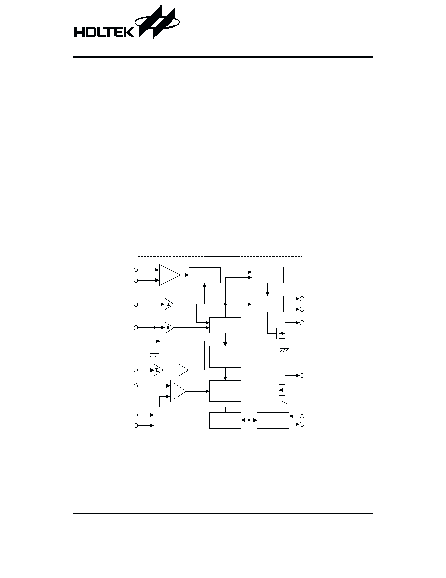
Block Diagram
Rev. 1.40
1
September 30, 2002
Features
·
Operating voltage: 3.5V~5.5V
·
Bell 202 FSK and V.23 demodulation
·
Ring detection input and output
·
Carrier detection output
·
Power down mode
·
High input sensitivity
·
HT9032C: 16-pin DIP/SOP package
HT9032D: 8-pin DIP/SOP package
Applications
·
Feature phones
·
Caller ID adjunct boxes
·
Fax and answering machines
·
Computer telephony interface products
·
ADSI products
General Description
The HT9032 calling line identification receiver is a low
power CMOS integrated circuit designed for receiving
physical layer signals transmitted according to Bellcore
TR-NWT-000030 and ITU-T V.23 specifications. The
primary application of this device is for products used to
receive and display the calling number, or message
waiting indicator sent to subscribers from the central of-
fice facilities. The device also provides a carrier detec-
tion circuit and a ring detection circuit for easier system
applications.
B a n d P a s s
. i l t e r
P o w e r U p
L o g i c
D e m o d u l a t o r
V a l i d D a t a
D e t e c t i o n
D O U T C
D O U T
I n t e r n a l
P o w e r U p
L o g i c
R i n g
A n a l y s i s
C i r c u i t
R e f e r e n c e
V o l t a g e
C l o c k
G e n e r a t o r
C D E T
R D E T
V S S
V D D
R D E T 2
T I P
R I N G
P D W N
R T I M E
R D E T 1
X 1
X 2
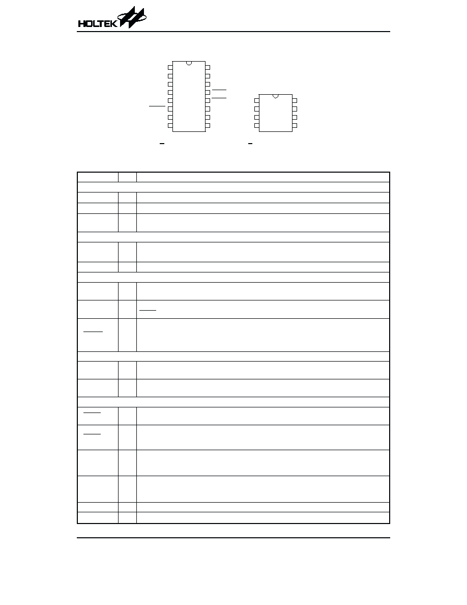
Pin Assignment
Pin Description
Pin Name
I/O
Description
Power Inputs
VDD
¾
Power-VDD is the input power for the internal logic.
VSS
¾
Ground-VSS is ground connection for the internal logic.
PDWN
I
A logic
²1² on this pin puts the chip in power down mode. When a logic ²0² is on this pin, the
chip in power up mode. This is a Schmitt trigger input.
Clock
X1
I
A crystal or ceramic resonator should be connected to this pin and X2.
This pin may be driven from an external clock source.
X2
O
A crystal or ceramic resonator should be connected to this pin and X1.
Ring Detections
RDET1
I
It detects ring energy on the line through an attenuating network and enables the oscillator and
ring detection. This is a Schmitt trigger input.
RDET2
I
It couples the ring signal to the precision ring detector through an attenuating network.
RDET=
²0² if a valid ring signal is detected. This is a Schmitt trigger input.
RTIME
I/O
An RC network may be connected to this pin in order to hold the pin voltage below 2.2V be-
tween the peaks of the ringing signal. This pin controls internal power up and activates the par-
tial circuitry needed to determine whether the incoming ring is valid or not. The input is a
Schmitt trigger input. The output cell structure is an NMOS output.
FSK Signal Inputs
TIP
I
This input pin is connected to the tip side of the twisted pair wires. It is internally biased to 1/2
V
DD
when the device is in power up mode. This pin must be DC isolated from the line.
RING
I
This input pin is connected to the ring side of the twisted pair wires. It is internally biased to 1/2
V
DD
when the device is in power up mode. This pin must be DC isolated from the line.
Detection Results
RDET
O
This open drain output goes low when a valid ringing signal is detected. When connected to
PDWN pin, this pin can be used for auto power up.
CDET
O
This open drain output goes low indicating that a valid carrier is present on the line. A hyster-
esis is built-in to allow for a momentary drop out of the carrier. When connected to PDWN pin,
this pin can be used for auto power up.
DOUT
O
This pin presents the output of the demodulator when chip in power up mode. This data stream
includes the alternate
²1² and ²0² pattern, the marking, and the data. At all other times, this pin
is held high.
DOUTC
O
This output presents the output of the demodulator when chip in power up mode and when an
internal validation sequence has been successfully passed. This data stream does not include
the alternate
²1² and ²0² pattern. This pin is always held high.
TEST
O
Output pin for testing purposes only.
NC
¾
No connection
HT9032C/HT9032D
Rev. 1.40
2
September 30, 2002
N C
T E S T
T I P
V D D
R T I M E
R D E T 1
X 2
P D W N
V S S
R I N G
C D E T
R D E T
X 1
R D E T 2
D O U T C
D O U T
H T 9 0 3 2 C
1 6 D I P - A / S O P - A
1
2
3
4
5
6
7
8
1 6
1 5
1 4
1 3
1 2
1 1
1 0
9
D O U T
T I P
V D D
R I N G
P D W N
X 2
V S S
X 1
1
2
3
4
8
7
6
5
H T 9 0 3 2 D
8 D I P - A / S O P - A
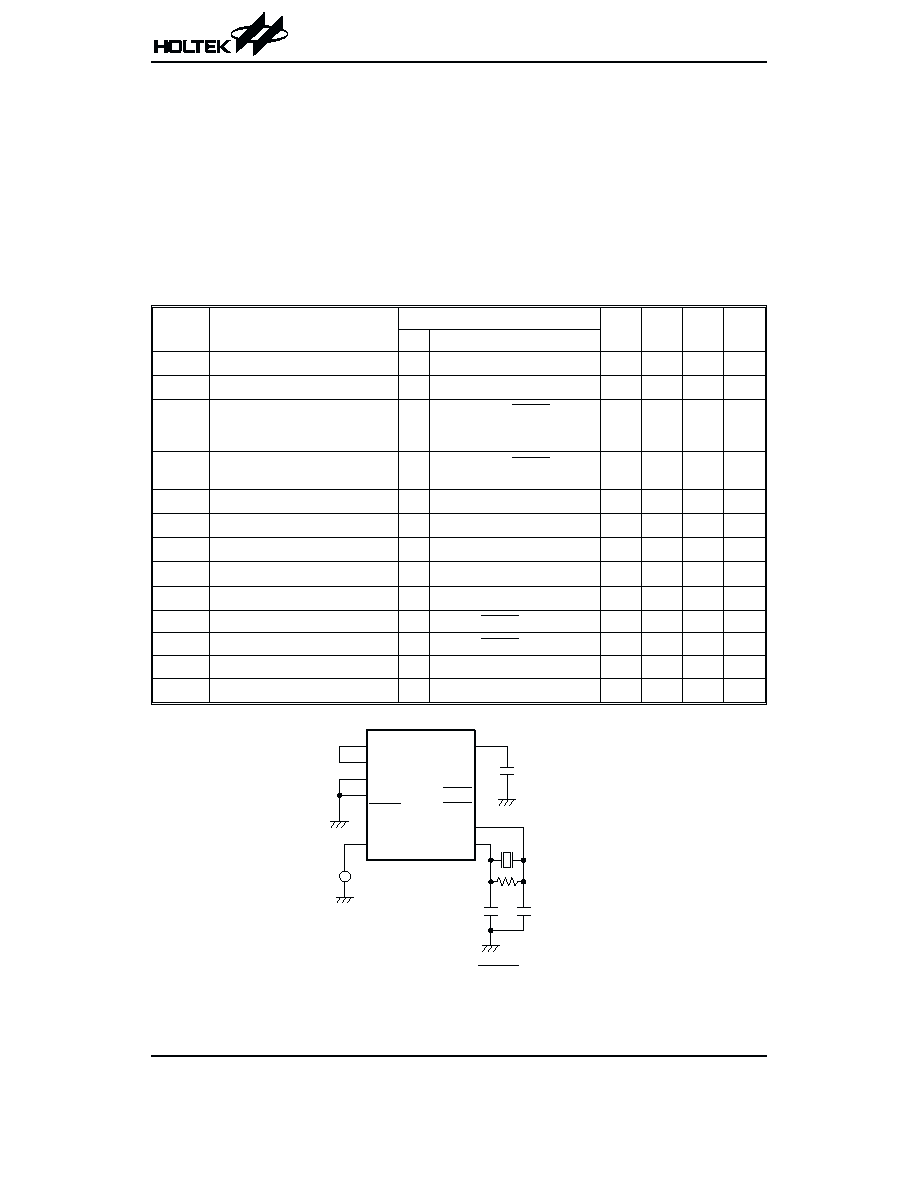
Absolute Maximum Ratings
Voltages are referenced to V
SS
, except where noted.
Supply Voltage .........................................
-0.5V to 6.0V
All Input Voltages.................................................25mW
Operating Temperature Range ...................0
°C to 70°C
Storage Temperature Range ................
-40°C to 150°C
Note: These are stress ratings only. Stresses exceeding the range specified under
²Absolute Maximum Ratings² may
cause substantial damage to the device. Functional operation of this device at other conditions beyond those
listed in the specification is not implied and prolonged exposure to extreme conditions may affect device reliabil-
ity.
D.C. Characteristics
Crystal=3.58MHz, Ta=0~70
°C
Symbol
Parameter
Test Conditions
Min.
Typ.
Max.
Unit
V
DD
Conditions
V
DD
Supply Voltage
¾
¾
3.5
5
5.5
V
I
DD1
Supply Current
5V
PDWN=0 (3.58MHz OSC on)
¾
3.2
5
mA
I
DD2
Supply Current
5V
PDWN=1 and RTIME=0
(3.58MHz OSC on and internal
circuits partially on)
¾
1.9
2.5
mA
I
STBY
Standby Current
5V
PDWN=1 and RTIME=1
(3.58MHz OSC off)
¾
¾
1
mA
V
IL
Input Voltage Logic 0
5V
¾
¾
¾
0.2V
V
DD
V
IH
Input Voltage Logic 1
5V
¾
0.8V
¾
¾
V
DD
I
OL
Output Voltage Logic 0
5V
I
OL
=1.6mA
¾
¾
0.1V
V
DD
I
OH
Output Voltage Logic 1
5V
I
OH
=0.8mA
0.9V
¾
¾
V
DD
I
IN
Input Leakage Current, All Inputs
5V
¾
-1
¾
1
mA
V
T
-
Input Low Threshold Voltage
5V
RDET1, RTIME, PDWN
2.0
2.3
2.6
V
V
T+
Input High Threshold Voltage
5V
RDET1, RTIME, PDWN
2.5
2.75
3.0
V
V
TRDET2
Input Threshold Voltage
5V
RDET2
1.0
1.1
1.2
V
R
IN
Input DC Resistance
5V
TIP, RING
¾
500
¾
k
W
HT9032C/HT9032D
Rev. 1.40
3
September 30, 2002
T I P
V D D
R T I M E
R D E T 1
X 2
P D W N
V S S
R I N G
C D E T
R D E T
X 1
R D E T 2
D O U T C
D O U T
H T 9 0 3 2 C
~
3 . 5 8 M H z
1 0 M W
3 0 p .
0 . 1 m .
S u p p l y c u r r e n t t e s t i n g : A l l , e x c e p t P D W N a n d R T I M E , u n w i r e d p i n s a r e l e f t f l o a t i n g .
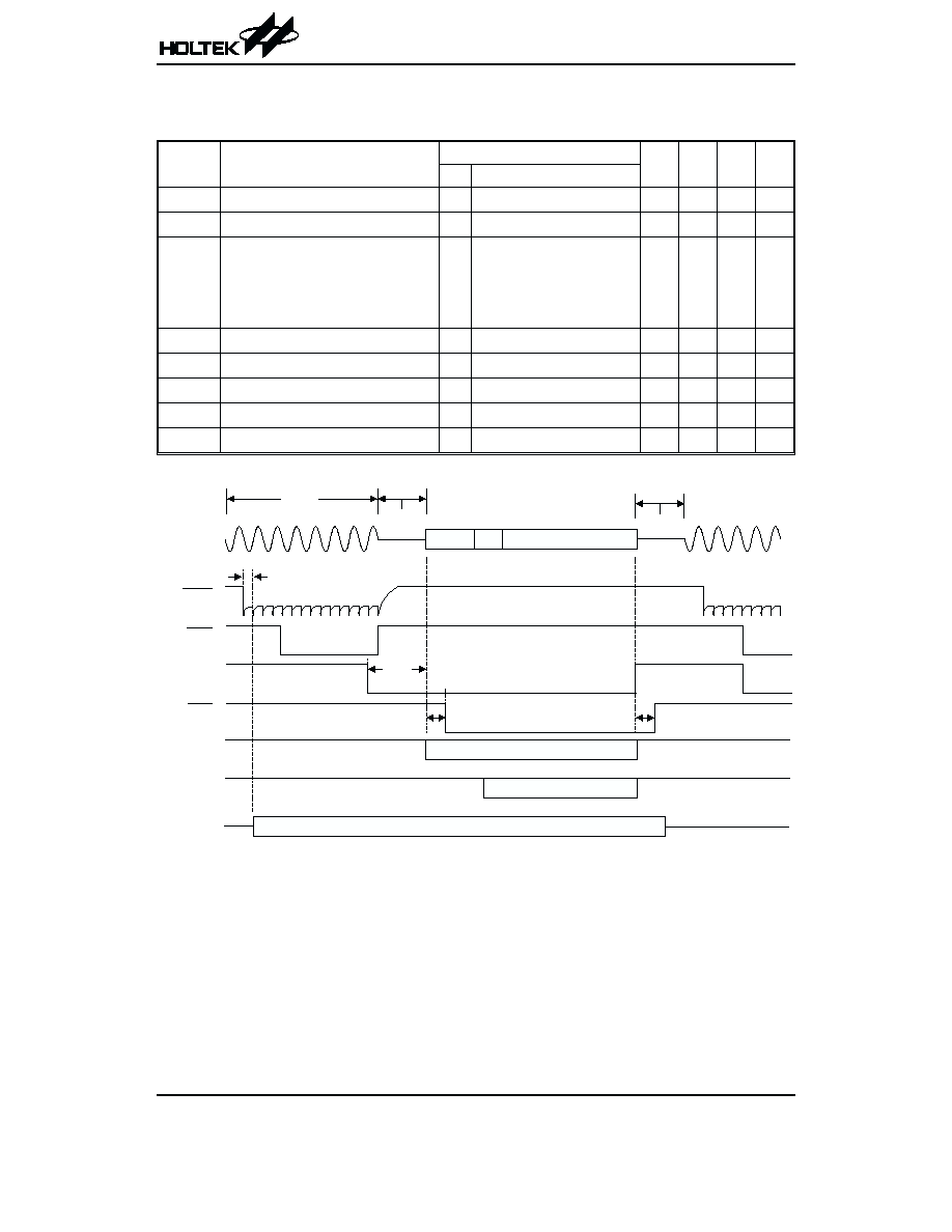
A.C. Characteristics
- FSK Detection
V
SS
=0V, Crystal=3.58MHz, Ta=0 to 70
°C, 0dBm=0.7746Vrms @ 600W
Symbol
Parameter
Test Conditions
Min.
Typ.
Max.
Unit
V
DD
Conditions
Input Sensitivity: TIP, RING
5V
-40
-45
¾
dBm
S/N
Signal to Noise Ratio
5V
¾
20
¾
dB
Band Pass Filter
60Hz
550Hz
2700Hz
3300Hz
5V
Frequency Response
Relative to 1700Hz @ 0dBm
¾
-64
-4
-3
-34
¾
dB
Carrier Detect Sensitivity
5V
¾
-48
¾
dBm
t
DOSC
Oscillator Start Up Time
5V
¾
¾
2
¾
ms
t
SUPD
Power Up to FSK Signal Set Up Time
5V
¾
15
¾
¾
ms
t
DAQ
Carrier Detect Acquisition Time
5V
¾
¾
14
¾
ms
t
DCH
End of Data to Carrier Detect High
5V
¾
8
¾
¾
ms
HT9032C/HT9032D
Rev. 1.40
4
September 30, 2002
R i n g S i g n a l
R T I M E
R D E T
P D W N
C D E T
D O U T
X 1
0 1 0 1 0 1 . .
D A T A
2 S e c
3 . 5 8 M H z
R a w D A T A
t
D O S C
t
D A Q
t
S U P D
t
D C H
D O U T C
C o o k e d D A T A
1
0 . 5 S e c
0 . 5 S e c
HT9032C/HT9032D
Rev. 1.40
5
September 30, 2002
Functional Description
The HT9032 is designed to be the physical layer de-
modulator for products targeted for the caller ID market.
The data signaling interface should conform to Bell 202,
which is described as follows:
·
Analog, phase coherent, frequency shift keying
·
Logical 1 (Mark)=1200+/
-12Hz
·
Logical 0 (Space)=2200+/
-22Hz
·
Transmission rate=1200bps
·
Data application=serial, binary, asynchronous
The interface should be arranged to allow simple data
transmission from the terminating central office, to the
CPE (Customer Premises Equipment), only when the
CPE is in an on-hook state. The data will be transmitted
in the silent period between the first and second power
ring before a voice path is established. The transmission
level from the terminating C.O. will be
-13.5dBm+/-1.0.
The worst case attenuation through the loop is expected
to be
-20dB. The receiver therefore, should have a sen-
sitivity of approximately
-34.5dBm to handle the worst
case installations. The ITU-T V.23 is also using the FSK
signaling scheme to transmit data in the general
switched telephone network. For mode 2 of the V.23, the
modulation rate and characteristic frequencies are listed
below:
·
Analog, phase coherent, frequency shift keying
·
Logical 1 (Mark)=1300Hz
·
Logical 0 (Space)=2100Hz
·
Transmission rate=1200bps
Since the band pass filter of the HT9032 can pass the
V.23 signal, hence the HT9032 also can demodulate the
V.23 signal.
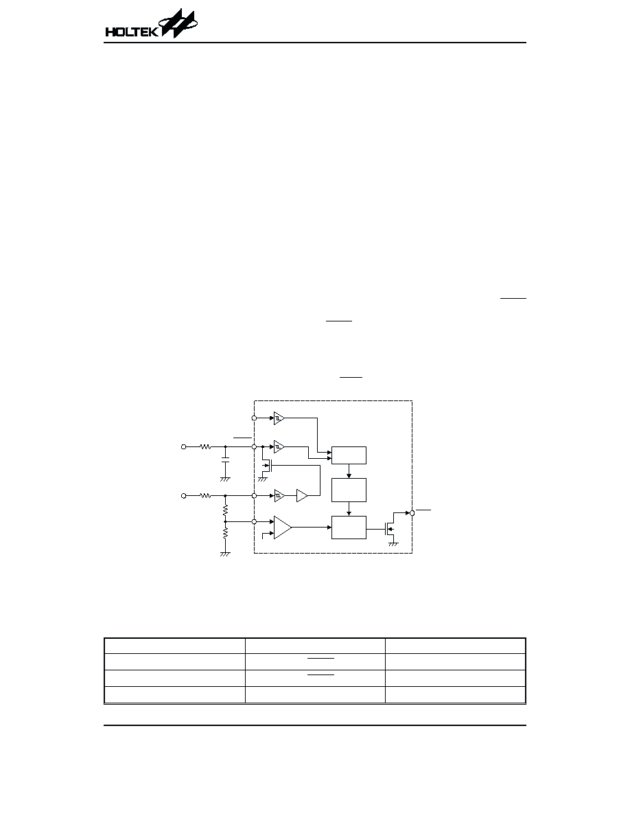
Ring detection
The data will be transmitted in the silent period between
the first and second power ring before a voice path is es-
tablished. The HT9032 should first detect a valid ring
and then perform the FSK demodulation. The typical
ring detection circuit of the HT9032 is depicted below.
The power ring signal is first rectified through a bridge
circuit and then sent to a resistor network that attenu-
ates the incoming power ring. The values of resistors
and capacitor given in the figure have been chosen to
provide a sufficient voltage at RDET1 pin to turn on the
Schmitt trigger input with approximately a 40 Vrms or
greater power ring input from tip and ring. When V
T+
of
the Schmitt is exceeded, the NMOS on the pin RTIME
will be driven to saturation discharging capacitor on
RTIME. This will initialize a partial power up, with only
the portions of the part involved with the ring signal anal-
ysis enabled, including RDET2 pin. With RDET2 pin en-
abled, a portion of the power ring above 1.2V is fed to
the ring analysis circuit. Once the ring signal is qualified,
the RDET pin will be sent low.
P o w e r U p
L o g i c
I n t e r n a l
P o w e r U p
L o g i c
R i n g
A n a l y s i s
C i r c u i t
1 . 2 V
R D E T 2
R D E T
R T I M E
V
D D
0 . 2 m .
2 7 0 k W
P D W N
R D E T 1
4 7 0 k W
1 8 k W
1 5 k W
T o
B r i d g e
Operation mode
There are three operation modes of the HT9032. They are power down mode, partial power up mode, and power up
mode. The three modes are classified by the following conditions:
Modes
Conditions
Current Consumption
Power down
PDWN=
²1² and RTIME=²1²
<1
mA
Partial power up
PDWN=
²1² and RTIME=²0²
1.9mA typically
Power up
PDWN=
²0²
3.2mA typically
Document Outline
- þÿ
- þÿ
- þÿ
- þÿ
- þÿ
- þÿ
- þÿ
- þÿ
- þÿ
- þÿ
- þÿ
- þÿ