 | ÐлекÑÑоннÑй компоненÑ: HT9315A | СкаÑаÑÑ:  PDF PDF  ZIP ZIP |
Äîêóìåíòàöèÿ è îïèñàíèÿ www.docs.chipfind.ru
HT9315 Series
15-Memory Tone/Pulse Dialer
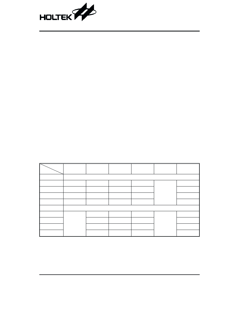
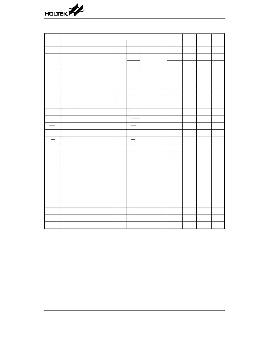
Selection Table
Function
Item
Lock
Function
Hold-Line
Hand-Free
LCD
Interface
Min.
Flash Time
Package
HT9315x
(Normal version)
HT9315A
¾
¾
¾
¾
98ms
18 DIP
HT9315B
¾
Ö
Ö
¾
22 SKDIP
HT9315C
¾
¾
¾
Ö
20 DIP
HT9315D
¾
Ö
Ö
Ö
24 SKDIP
HT9315xL
(Mechanical and Keyboard Operated Lock Version)
HT9315AL
Lock 0
Lock 0, 9
Lock All
Keyboard
Operated Lock
¾
¾
¾
98ms
18 DIP
HT9315BL
Ö
Ö
¾
22 SKDIP
HT9315CL
¾
¾
Ö
20 DIP
HT9315DL
Ö
Ö
Ö
24 SKDIP
Rev. 1.20
1
October 1, 2002
Features
·
Universal specification
·
Operating voltage: 2.0V~5.5V
·
Low standby current
·
Low memory retention current: 0.1
mA (Typ.)
·
Tone/pulse switchable
·
Interface with LCD driver
·
32 digits for redialing
·
32 digits for the SA memory dialing
·
One-key redialing
·
Pause and P
®T key for PBX
·
4
´5 keyboard matrix
·
3.58MHz crystal or ceramic resonator
·
Hand-free control
·
Hold-line control
·
Pause, P
®T can be saved for redialing
·
Lock function
·
Keytone function
·
Resistor options:
-
M/B ratio
-
Flash function and flash time (86ms~600ms)
-
Pause and P
®T duration
-
Pulse number
-
Keyboard operated IDD lock function
-
Keyboard form
·
HT9315A/HT9315AL: 18-pin DIP package
HT9315B/HT9315BL: 22-pin SKDIP package
HT9315C/HT9315CL: 20-pin DIP package
HT9315D/HT9315DL: 24-pin SKDIP package
General Description
The HT9315 series tone/pulse dialers are CMOS LSIs for
telecommunication systems. They are designed to meet
various dialing specifications through resistor option ma-
trix.
The HT9315 series are offered in two different ver-
sions. They are HT9315x normal version and
HT9315xL lock version, with keyboard-operated IDD
lock function. The two versions also supply the follow-
ing functions: Hold-line, Hand-free and LCD dialing
number display interface, all of which are suitable for
feature phone applications.
Patent Number: 64097, 86474, 113235(R.O.C.), 5424740(U.S.A.)
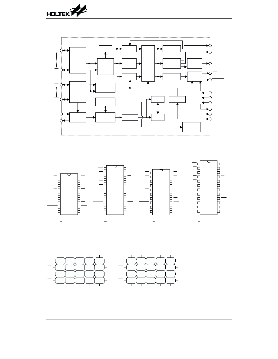
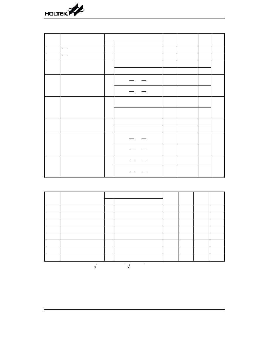
Block Diagram
Pin Assignment
HT9315x/xL version
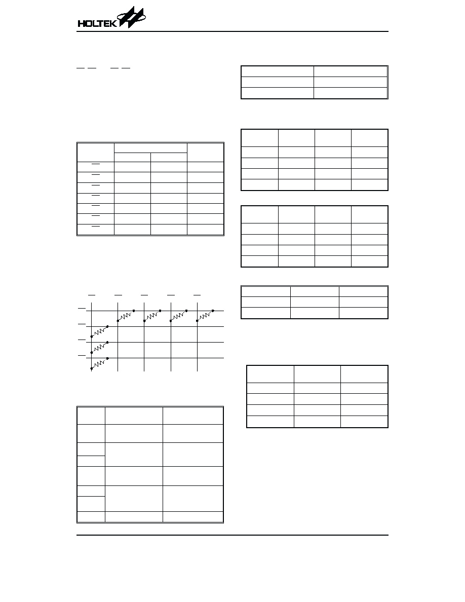
Keyboard Information
HT9315 Series
Rev. 1.20
2
October 1, 2002
C 1
R 1
P O
H K S
H D I
K e y
C o l u m n
. S M
K e y
. u n c t i o n
E n c o d e r
E n c o d e r
C o n t r o l
W R M
C o u n t e r
A D D R L
K e y R o w
S R A M
D e b o u n c e
D i v i d e r
C l o c k
G e n e r a t o r
M / B
. l a s h
T i m e r
C h e c k
T o n e
E n c o d e r
C o n v e r t e r
M o d e I n
H D / H .
T o n e
O u t
P u l s e
O u t
D T M .
H . I
M O D E
H . O
H D O
D O U T
C L O C K
X M U T E
C 5
R 4
X 1
X 2
K e y t o n e
G e n e r a t o r
2 4
2 3
2 2
2 1
2 0
1 9
1 8
1 7
1 6
1 5
1 4
1 3
1
2
3
4
5
6
7
8
9
1 0
1 1
1 2
H D O
R 4
R 3
R 2
R 1
M O D E
D T M .
P O
H K S
V D D
H . O
C L O C K
1 8
1 7
1 6
1 5
1 4
1 3
1 2
1 1
1 0
1
2
3
4
5
6
7
8
9
H T 9 3 1 5 A / A L
1 8 D I P - A
R 4
R 3
R 2
R 1
M O D E
D T M .
P O
H K S
V D D
2 2
2 1
2 0
1 9
1 8
1 7
1 6
1 5
1 4
1 3
1 2
1
2
3
4
5
6
7
8
9
1 0
1 1
H D O
R 4
R 3
R 2
R 1
M O D E
D T M .
P O
H K S
V D D
H . O
2 0
1 9
1 8
1 7
1 6
1 5
1 4
1 3
1 2
1 1
1
2
3
4
5
6
7
8
9
1 0
R 4
R 3
R 2
R 1
M O D E
D T M .
P O
H K S
V D D
C L O C K
C 1
C 2
C 3
C 4
C 5
X 1
X 2
X M U T E
V S S
H D I
C 1
C 2
C 3
C 4
C 5
X 1
X 2
X M U T E
V S S
H . I
C 1
C 2
C 3
C 4
C 5
X 1
X 2
X M U T E
V S S
D O U T
H D I
C 1
C 2
C 3
C 4
C 5
X 1
X 2
X M U T E
V S S
H . I
D O U T
H T 9 3 1 5 B / B L
2 2 S K D I P - A
H T 9 3 1 5 C / C L
2 0 D I P - A
H T 9 3 1 5 D / D L
2 4 S K D I P - A
1
4
7
* / T
2
5
8
0
3
6
9
#
E M 1
E M 2
E M 3
S T
1
4
7
* / T
2
5
8
0
3
6
9
#
P
.
A
R
C 5
. o r m B
C 4
C 1
C 2
C 3
C 5
. o r m A
C 4
C 1
C 2
C 3
R 4
R 3
R 2
R 1
R 4
R 3
R 2
R 1
E M 1
E M 2
E M 3
S T
S A
.
A
R / P
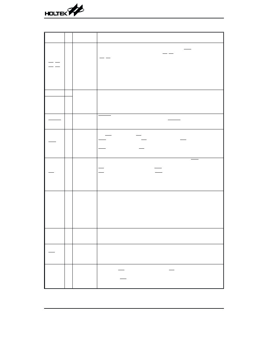
Pin Description
Pin Name
I/O
Internal
Connection
Description
C1~C5
R1~R4
I/O
CMOS
IN/OUT
These pins form a 4
´5 keyboard matrix which can perform keyboard input detection
and dialing specification setting functions. When on-hook (HKS=high) all the pins are
set high. While off-hook the column group (C1~C5) remains low and the row group
(R1~R4) is set high for key input detection.
An inexpensive single contact 4
´5 keyboard can be used as an input device.
Pressing a key connects a single column to a single row, and actuates the system os-
cillator that results in a dialing signal output. If more than two keys are pressed at the
same time, no response occurs. The key-in debounce time is 20ms. Refer to the key-
board information for keyboard arrangement and to the functional description for dial-
ing specification selection.
X1
I
OSCILLATOR
The system oscillator consists of an inverter, a bias resistor and the necessary
load capacitor on chip. Connecting a standard 3.579545MHz crystal or ceramic
resonator to the X1 and X2 terminals can implement the oscillator function. The
oscillator is turned off in the standby mode, and is actuated whenever a keyboard
entry is detected.
X2
O
XMUTE
O
NMOS OUT
XMUTE is an NMOS open drain structure pulled to VSS during dialing signal
transmission. Otherwise, it is an open circuit. XMUTE is used to mute the speech
circuit when transmitting the dial signal.
HKS
I
CMOS IN
This pin is used to monitor the status of the hook-switch and its combination with
HFI/HDI can control the PO pin output to make or break the line.
HKS=VDD: On-hook state (PO=low). Except for HFI/HDI
(hand-free/hold-line control input), other functions are all disabled.
HKS=VSS: Off-hook state (PO=high). The chip is in the standby mode and ready to
receive the key input.
PO
O
CMOS OUT
This pin is a CMOS output structure which by receiving the HKS and HFO/HDO
signals, control the dialer to connect or disconnect the telephone line.
PO outputs a low to break line when HKS is high (on-hook) and HFO/HDO is low.
PO outputs a high to make line when HKS is low (off-hook) or HFO is high or HDO
is high.
During the off-hook state, this pin also outputs the dialing pulse train in pulse
mode dialing. While in the tone mode, this pin is always high.
MODE
I/O
CMOS
IN/OUT
This is a three-state input/output pin, use for dialing mode selection, either Tone
mode or Pulse mode, 10pps/20pps
MODE=VDD: Pulse mode, 10pps
MODE=OPEN: Pulse mode, 20pps
MODE=VSS: Tone mode
During the pulse mode dialing, switching this pin to the tone mode changes the
subsequent digit entry to tone mode. When the chips are in tone mode, switching
to pulse mode will also be recognized.
DTMF
O
CMOS OUT
This pin is active only when the chip transmits tone dialing signals. Otherwise, it
always outputs a low. The pin outputs tone signals to drive the external transmitter
amplifier circuit. The load resistor should not be less than 5k
W.
HDI
I
CMOS IN
Pull-High
This pin is a Schmitt trigger input structure. Active low. Applying a negative going
pulse to this pin can toggle the HDO output once.
An external RC network is recommended for input debouncing. The pull-high re-
sistance is 200k
W typ.
HDO
O
CMOS OUT
The HDO is a CMOS output structure. Its output is toggle- controlled by a negative
transition on HDI. When HDO is toggled high, PO keeps high to hold the line. The
hold function can be released by setting HFO high or by an on/off hook operation
or by another HDI input. Refer to the functional description for the hold-line func-
tion.
HT9315 Series
Rev. 1.20
3
October 1, 2002
Pin Name
I/O
Internal
Connection
Description
HFI
I
CMOS IN
Pull-Low
This pin is a Schmitt trigger input structure. Active high. Applying a positive pulse
to HFI can toggle the HFO once and hence control the hand-free function. The
pull-low resistance of HFI is 200k
W typ.
An external RC network is recommended for input debouncing.
HFO
O
CMOS OUT
The HFO is a CMOS output structure. Its output is toggle- controlled by a positive
transition on HFI pin. When HFO is high, the hand-free function is enabled and PO
outputs a high to connect the line.
The hand-free function can be released by setting HDO high or by an on-off-hook op-
eration or by another HFI input. Refer to the functional description for the hand-free
functional operation.
DOUT
O
NMOS OUT
NMOS open drain output pin. It outputs the BCD code of the dialing digits to the
LCD driver chip (HT16XX series) or MCU for dialing number display. Refer to the
functional description for the detailed timing.
CLOCK
O
NMOS OUT
NMOS open drain output. When dialing, it outputs a series of pulse trains for
DOUT data synchronization. DOUT data is valid at the falling edge of the clock.
VDD
¾
¾
Positive power supply, 2.0V~5.5V for normal operation
VSS
¾
¾
Negative power supply, ground
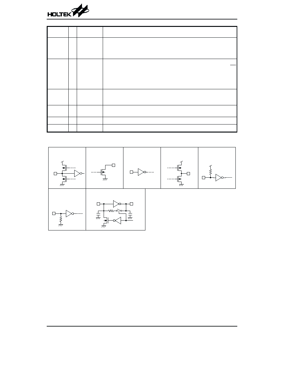
Approximate internal connection circuits
Absolute Maximum Ratings
Supply Voltage ...........................................
-0.3V to 6V
Input Voltage .............................. V
SS
-0.3 to V
DD
+0.3V
Storage Temperature ...........................
-50°C to 125°C
Operating Temperature ..........................
-20°C to 75°C
Note: These are stress ratings only. Stresses exceeding the range specified under
²Absolute Maximum Ratings² may
cause substantial damage to the device. Functional operation of this device at other conditions beyond those
listed in the specification is not implied and prolonged exposure to extreme conditions may affect device reliabil-
ity.
HT9315 Series
Rev. 1.20
4
October 1, 2002
N M O S O U T
V D D
C M O S I N / O U T
C M O S I N
P u l l - L o w
C M O S I N
P u l l - H i g h
C M O S I N
O S C I L L A T O R
X 1
X 2
E N
1 0 M
2 0 P
1 0 P
C M O S O U T
V D D
Electrical Characteristics
F
OSC
=3.5795MHz, Ta=25
°C
Symbol
Parameter
Test Conditions
Min.
Typ.
Max.
Unit
V
DD
Conditions
V
DD
Operating Voltage
¾
¾
2
¾
5.5
V
I
DD
Operating Current
2.5V
Pulse
Off-hook
Keypad entry
No load
¾
0.2
1
mA
Tone
¾
0.6
2
mA
I
STB
Standby Current
1V
On-hook, no load
No entry
¾
¾
1
mA
V
R
Memory Retention Voltage
¾
¾
1
5.5
V
I
R
Memory Retention Current
1V
On-hook
¾
0.1
0.2
mA
V
IL
Input Low Voltage
¾
¾
V
SS
¾
0.2V
DD
V
V
IH
Input High Voltage
¾
¾
0.8V
DD
¾
V
DD
V
I
XMO
XMUTE Leakage Current
¾
V
XMUTE
=12V, No entry
¾
¾
1
mA
I
OLXM
XMUTE Sink Current
2.5V
V
XMUTE
=0.5V
1
¾
¾
mA
I
HKS
HKS Pin Input Current
2.5V
V
HKS
=2.5V
¾
¾
0.1
mA
R
HFI
HFI Pull-Low Resistance
2.5V
V
HFI
=2.5V
¾
200
¾
k
W
R
HDI
HDI Pull-High Resistance
2.5V
V
HDI
=0V
¾
200
¾
k
W
I
OH1
Keypad Pin Source Current
2.5V
V
OH
=0V
-4
¾
-40
mA
I
OL1
Keypad Pin Sink Current
2.5V
V
OL
=2.5V
200
400
¾
mA
I
OH2
HFO Pin Source Current
2.5V
V
OH
=2V
-1
¾
¾
mA
I
OL2
HFO Pin Sink Current
2.5V
V
OL
=0.5V
1
¾
¾
mA
I
OH3
HDO Pin Source Current
2.5V
V
OH
=2V
-1
¾
¾
mA
I
OL3
HDO Pin Sink Current
2.5V
V
OL
=0.5V
1
¾
¾
mA
T
FP
Pause Time After Flash
¾
Control key
¾
0.2
¾
s
Digit key
¾
1
¾
T
RP
One-key Redialing Pause Time
¾
One-key redialing
¾
1
¾
s
T
DB
Key-in Debounce Time
¾
¾
¾
20
¾
ms
T
BRK
Break Time for One-key Redialing
¾
One-key redialing
¾
1.2
¾
s
F
OSC
System Frequency
¾
Crystal=3.5795MHz
3.5759
3.5795
3.5831
MHz
HT9315 Series
Rev. 1.20
5
October 1, 2002
Pulse Mode Electrical Characteristics
F
OSC
=3.5795MHz, Ta=25
°C
Symbol
Parameter
Test Conditions
Min.
Typ.
Max.
Unit
V
DD
Conditions
I
POH
PO Output Source Current 2.5V V
OH
=2V
-0.2
¾
¾
mA
I
POL
PO Output Sink Current
2.5V V
OL
=0.5V
0.2
0.6
¾
mA
PR
Pulse Rate
¾
MODE pin is connected to V
DD
¾
10
¾
pps
MODE pin is opened
¾
20
¾
M/B
Make/Break Ratio
¾
A resistor is linked
between R2 and C1
¾
33:66
¾
%
No resistor is linked
between R2 and C1
¾
40:60
¾
T
PDP
Pre-digit-pause Time
¾
M/B ratio=40:60
¾
40 (10pps)
20 (20pps)
¾
ms
M/B ratio=33:66
¾
33 (10pps)
17 (20pps)
¾
T
IDP
Inter-digit-pause Time
¾
Pulse rate=10pps
¾
800
¾
ms
Pulse rate=20pps
¾
500
¾
T
M
Pulse Make Duration
¾
A resistor is linked
between R2 and C1
¾
33 (10pps)
17 (20pps)
¾
ms
No resistor is linked
between R2 and C1
¾
40 (10pps)
20 (20pps)
¾
T
B
Pulse Break Duration
¾
A resistor is linked
between R2 and C1
¾
66 (10pps)
33 (20pps)
¾
ms
No resistor is linked
between R2 and C1
¾
60 (10pps)
30 (20pps)
¾
Tone Mode Electrical Characteristics
F
OSC
=3.5795MHz, Ta=25
°C
Symbol
Parameter
Test Conditions
Min.
Typ.
Max.
Unit
V
DD
Conditions
V
TDC
DTMF Output DC Level
¾
¾
0.45V
DD
¾
0.7V
DD
V
I
TOL
DTMF Sink Current
2.5V V
DTMF
=0.5V
0.1
¾
¾
mA
V
TAC
DTMF Output AC Level
¾ Row group, R
L
=5k
W
0.12
0.155
0.18
Vrms
R
L
DTMF Output Load
2.5V THD
£-23dB
5
¾
¾
k
W
A
CR
Column Pre-emphasis
2.5V Row group=0dB
1
2
3
dB
THD
Tone Signal Distortion
2.5V R
L
=5k
W
¾
-30
-23
dB
T
TMIN
Minimum Tone Duration
¾ Auto-redial
¾
82.5
¾
ms
T
ITPM
Minimum Inter-tone Pause
¾ Auto-redial
¾
85.5
¾
ms
THD (Distortion) (dB) = 20 log
(
)
V1
V2
... Vn / Vi
Vh
2
2
2
2
2
+
+ +
+
Vi, Vh: Row group and column group signals
V1, V2, ... Vn: Harmonic signals (BW=300Hz~3500Hz)
HT9315 Series
Rev. 1.20
6
October 1, 2002
HT9315 Series
Rev. 1.20
7
October 1, 2002
Functional Description
Keyboard matrix
C1~C5 and R1~R4 form a keyboard matrix. Together
with a standard 4
´5 keyboard, the keyboard matrix is
used for dialing entries. In addition, the keyboard ma-
trix provides resistor option for different dialing specifi-
cation selections. The keyboard arrangement for each
of the HT9315 series are shown in the Keyboard Infor-
mation.
Tone frequency
Tone Name
Output Frequency (Hz)
% Error
Specified
Actual
R1
697
699
+0.29%
R2
770
766
-0.52%
R3
852
847
-0.59%
R4
941
948
+0.74%
C1
1209
1215
+0.50%
C2
1336
1332
-0.30%
C3
1477
1472
-0.34%
Note:% Error does not contain the crystal frequency drift
Dialing specification selection
Various dialing specifications can be selected by adding
resistors across keyboard matrix pins. The allowable
option resistor connections are shown on the table.
All the resistors are 330k
W. The resistor option functions
and the default specifications without option resistors
are listed below.
Option
Resistor
Option
Function
Default
(No Resistor)
R
K12
Make/Break Ratio
Selection
40:60
R
K13
Flash Function and
Flash Time Selection
Flash= control function
Flash time= 600ms
R
K14
R
K21
Pause & P
®T
Duration Selection
T
P
= 3.6s
T
P
®T
= 3.6s
R
K31
Pulse Number
Selection or IDD
Lock Selection
N or Keyboard
Operated Lock
R
K41
R
K51
Keypad Form
FormA
M/B ratio selection table
R
K12
M/B Ratio (%)
No
40:60
Yes
33.3:66.6
Flash function/time (duration) selection table
·
HT9315x
R
K13
R
K14
Flash
Function
Flash
Time (T
F
)
No
No
Control
600ms
No
Yes
Digit
600ms
Yes
No
Digit
98ms
Yes
Yes
Digit
300ms
·
HT9315xL
R
K13
R
K14
Flash
Function
Flash
Time (T
F
)
No
No
Control
600ms
No
Yes
Control
600ms
Yes
No
Control
98ms
Yes
Yes
Control
300ms
Pause and P
®T duration selection table
R
K21
T
P
(sec)
T
P
®T
(sec)
No
3.6
3.6
Yes
2
1
Pulse number selection table
·
This table shows pulse number selections for
HT9315x. The table for HT9315xL is used to select
IDD lock function.
R
K31
R
K41
Pulse
Number
No
No
N
No
Yes
N+1
Yes
No
10
-N
Yes
Yes
¾
K 5 1
R
K 1 4
R
K 1 2
R
K 2 1
R
K 3 1
R
K 4 1
R
C 1
C 2
C 3
C 4
K 1 3
R
R 1
R 2
R 3
R 4
C 5
HT9315 Series
Rev. 1.20
8
October 1, 2002
Pulse number table
Keypad
Output Pulse Number
Digit Key
Normal N
New
Zealand
(10N)
Sweden/
Denmark
(N+1)
1
1
9
2
2
2
8
3
3
3
7
4
4
4
6
5
5
5
5
6
6
6
4
7
7
7
3
8
8
8
2
9
9
9
1
10
0
10
10
1
*/T
P
®T
P
®T
P
®T
#
Ignored
Ignored
Ignored
The keyboard arrangement selection table
R
K51
Keypad Form
No
Form A (see keyboard information)
Yes
Form B (see keyboard information)
Hand-free function operation
·
Hand-free function execution
When HFO is low, a rising edge triggers the HFI, en-
abling the Hand-free function (HFO becomes high).
·
Reset Hand-free function
When HFO is high, the Hand-free function is enabled
and can be reset by:
¨
Off-hook
¨
Applying a rising edge to HFI
¨
Changing the HDO pin from low to high
·
Hand-free function table
Hold-line function operation
·
Hold-line function execution
When HDO is low, a falling edge triggers the HDI, en-
abling the Hold-line function (HDO becomes high).
The XMUTE remains low when HDO is high.
·
Reset Hold-line function
When HDO is high, the Hold-line function is enabled
and can be reset by:
¨
Off-hook
¨
Applying a falling edge to HDI
¨
Changing the HFO pin from low to high
·
Hold-line function table
DOUT BCD code
When dialing, the corresponding 4-bit BCD codes are
serially presented on DOUT from MSB to LSB. The data
of DOUT is valid at the falling edge of the CLOCK pin.
The following table lists the BCD codes corresponding
to the keyboard input.
Key-In
BCD Code
Key-In
BCD Code
1
0001
8
1000
2
0010
9
1001
3
0011
0
1010
4
0100
*/T
1101
5
0101
#
1100
6
0110
F
1011
7
0111
P
1110
C u r r e n t S t a t e
I n p u t
N e x t S t a t e
H K S
H
H
H
H
L
L
L
L
X
H . O
L
L
H
X
L
L
H
X
X
H D O
X
X
X
L
X
X
L
X
L
H . I
L
L
L
L
L
H K S
A n
A n
A n
L
A n
A n
A n
H
A n
H . O
L
H
L
L
L
H
L
A n
L
H D O
A n
L
A n
L
A n
L
A n
A n
H
H D I
H
H
H
H
H
H
H
H
H :
L :
L o g i c H I G H
L o g i c L O W
X :
A n :
D o n ' t c a r e
U n c h a n g e d
:
:
R i s i n g e d g e
. a l l i n g e d g e
C u r r e n t S t a t e
I n p u t
N e x t S t a t e
H K S
H
H
H
H
L
L
L
L
X
H D O
L
L
H
X
L
L
H
X
X
H . O
X
X
L
X
X
X
L
X
L
H D I
H
H
H
H
H
H K S
A n
A n
A n
L
A n
A n
A n
H
A n
H D O
L
H
L
L
L
H
L
A n
L
H . O
A n
L
A n
L
A n
L
A n
A n
H
H . I
L
L
L
L
L
L
L
L
H :
L :
L o g i c H I G H
L o g i c L O W
X :
A n :
D o n ' t c a r e
U n c h a n g e d
:
:
R i s i n g e d g e
. a l l i n g e d g e
HT9315 Series
Rev. 1.20
9
October 1, 2002
LOCK function
The function aims to detect locked dialing number to
prevent a long distance call. The dialing output of the
chip is disabled if the first input key after on-off-hook is
the locked number when the lock function is enabled.
The lock function selection is listed below. This function
is implemented on the HT9315xL. The HT9315x does
not support this function.
R
K31
R
K41
Function
No
No
Keyboard operated IDD lock
No
Yes
Lock 0
Yes
No
Lock 0, 9
Yes
Yes
All keys are locked
Key definition
·
0,1,2,3,4,5,6,7,8,9 keys
These are dialing number input keys for both the pulse
mode and the tone mode operations.
·
*/T
This key executes the P
®T function and waits a T
P
®T
duration in the pulse mode. On the other hand, the
*/T
key executes the
* function in the tone mode.
·
#
This is a dialing signal key for the tone mode only, no
response in the pulse mode.
·
SA
Pressing this key can save the preceding dialing tele-
phone numbers. The saved number is redialed if it is
pressed again. SA will also redial the saved number if
it is the first key pressed at the off-hook state. During
the dialing signal transmission, the SA key is inhibited.
·
F
The flash key can be selected as a digit or as a control
key by the option resistors R
K13
& R
K14
. Pressing the F
key will force the PO pin to be low for the T
F
duration and
is then followed by T
FP
(sec). T
F
can also be selected by
R
K13
, R
K14
.
·
P
Pause key. The execution of this key pauses the out-
put for the T
P
duration. T
P
can be selected by R
K21
.
·
R
Redial key. Executes redialing as well as one-key re-
dial function.
·
ST
Store key. The execution of this key actuates the store
memory function with (or without) dialing output and it
can store lock number with personal code in IDD lock
operation. During the dialing signal transmission, the
ST key is inhibited.
·
R/P
Redial and pause function key. If it is pressed as the
first key after off-hook, this key executes the redial
function. Otherwise, it works as the pause key.
·
EM1~EM3
One-touch memory dialing key. For speed-calling
convenience, they provide memory dialing in either
pulse or tone mode.
·
A
Auto key. When this key is pressed before pressing
any one of the digital keys (0~9) it executes the
two-touch memory function.
Keyboard operation
The following operations are described under an on/off- hook or on-hook condition with the hand-free active condition.
HT9315 Series
Rev. 1.20
10
October 1, 2002
K e y b o a r d i n p u t : D 1 D 2 . . . D n
- P u l s e m o d e
( a ) w i t h o u t * / T
D i a l i n g o u t p u t : D 1 D 2 . . . D n
R M : D 1 D 2 . . . D n
S A M : U n c h a n g e d
( b ) w i t h * / T
D i a l i n g o u t p u t : D 1 D 2 . . . D n T
P T
D n + 1 . . . D m
R M : D 1 D 2 . . . D n * / T D n + 1 . . . D m
S A M : U n c h a n g e d
T o n e
P u l s e
· N o r m a l d i a l i n g
K e y b o a r d i n p u t : D 1 D 2 . . . D n * / T D n + 1 . . .
D m
( a ) w i t h o u t * / T
D i a l i n g o u t p u t : D 1 D 2 . . . D n
R M : D 1 D 2 . . . D n
S A M : U n c h a n g e d
( b ) w i t h * / T
D i a l i n g o u t p u t : D 1 D 2 . . . D n * D n + 1 . . . D m
R M : D 1 D 2 . . . D n * D n + 1 . . . D m
S A M : U n c h a n g e d
- T o n e m o d e
( a ) w i t h o u t * / T
D i a l i n g o u t p u t : D 1 D 2 . . . D n
R M : U n c h a n g e d
S A M : U n c h a n g e d
R M c o n t e n t s : D 1 D 2 . . . D n
( b ) w i t h * / T
D i a l i n g o u t p u t : D 1 D 2 . . . D n T
P T
D n + 1 . . . D m
R M : U n c h a n g e d
S A M : U n c h a n g e d
R M c o n t e n t s : D 1 D 2 . . . D n * / T D n + 1 . . . D m
D i a l i n g o u t p u t : D 1 D 2 . . . D n
R M : U n c h a n g e d
S A M : U n c h a n g e d
R M c o n t e n t s : D 1 D 2 . . . D n
( b ) w i t h * / T
D i a l i n g o u t p u t : D 1 D 2 . . . D n * D n + 1 . . . D m
R M : U n c h a n g e d
S A M : U n c h a n g e d
R M c o n t e n t s : D 1 D 2 . . . D n * / T D n + 1 . . . D m
- P u l s e m o d e
- T o n e m o d e
P u l s e
T o n e
· R e d i a l
K e y b o a r d i n p u t : D 1 D 2 . . . D n * / T D n + 1 . . .
D m
( a ) w i t h o u t * / T
K e y b o a r d i n p u t : D 1 D 2 . . . D n
K e y b o a r d i n p u t : [ R o r R / P ]
K e y b o a r d i n p u t : [ R o r R / P ]
K e y b o a r d i n p u t : [ R o r R / P ]
K e y b o a r d i n p u t : [ R o r R / P ]
N o t e : T h e m a x i m u m c a p a c i t y o f t h e R M m e m o r y i s 3 2 d i g i t s . W h e n m o r e t h a n 3 2 d i g i t s a r e e n t e r e d ,
t h e s i g n a l i s t r a n s m i t t e d b u t t h e r e d i a l f u n c t i o n i s i n h i b i t e d .
HT9315 Series
Rev. 1.20
11
October 1, 2002
D m S A
K e y b o a r d i n p u t : D 1 D 2 . . . D n * / T D n + 1 . . .
D m S A
K e y b o a r d i n p u t : D 1 D 2 . . . D n * / T D n + 1 . . .
D m
R
K e y b o a r d i n p u t : D 1 D 2 . . . D n * / T D n + 1 . . .
K e y b o a r d i n p u t : D 1 D 2 . . . D n R
( a ) w i t h o u t * / T
D i a l i n g o u t p u t : D 1 D 2 . . . D n T
B R K
T
R P
R M : D 1 D 2 . . . D n
S A M : U n c h a n g e d
( b ) w i t h * / T
R M : D 1 D 2 . . . D n * / T D n + 1 . . . D m
S A M : U n c h a n g e d
( a ) w i t h o u t * / T
R M : D 1 D 2 . . . D n
S A M : U n c h a n g e d
( b ) w i t h * / T
- T o n e m o d e
- P u l s e m o d e
P u l s e
T
B R K
T
R P
D 1 D 2 . . . D n T
P T
P u l s e
D i a l i n g o u t p u t : D 1 D 2 . . . D n * D n + 1 . . . D m
R M : D 1 D 2 . . . D n * D n + 1 . . . D m
S A M : U n c h a n g e d
T
B R K
T
R P
D 1 D 2 . . . D n * D n + 1
. . . D m
T o n e
D i a l i n g o u t p u t : D 1 D 2 . . . D n T
P
T D n + 1 . . . D m
T o n e
· O n e - k e y r e d i a l
( a ) w i t h o u t * / T
D i a l i n g o u t p u t : D 1 D 2 . . . D n
R M : D 1 D 2 . . . D n
S A M : D 1 D 2 . . . D n
( b ) w i t h * / T
R M : D 1 D 2 . . . D n * / T D n + 1 . . . D m
S A M : D 1 D 2 . . . D n * / T D n + 1 . . . D m
( a ) w i t h o u t * / T
D i a l i n g o u t p u t : D 1 D 2 . . . D n
R M : D 1 D 2 . . . D n
S A M : D 1 D 2 . . . D n
( b ) w i t h * / T
D i a l i n g o u t p u t : D 1 D 2 . . . D n * D n + 1 . . . D m
R M : D 1 D 2 . . . D n * D n + 1 . . . D m
S A M : D 1 D 2 . . . D n * D n + 1 . . . D m
- P u l s e m o d e
- T o n e m o d e
D i a l i n g o u t p u t : D 1 D 2 . . . D n T
P T
D n + 1 . . . D m
T o n e
P u l s e
· S A c o p y
D 1 D 2 . . . D n
D i a l i n g o u t p u t : D 1 D 2 . . . D n T
B R K
T
R P
D 1 D 2
. . . D n
D n + 1 . . . D m
K e y b o a r d i n p u t : D 1 D 2 . . . D n R
D m
R
K e y b o a r d i n p u t : D 1 D 2 . . . D n * / T D n + 1 . . .
K e y b o a r d i n p u t : D 1 D 2 . . . D n S A
K e y b o a r d i n p u t : D 1 D 2 . . . D n S A
N o t e : T h e m a x i m u m c a p a c i t y o f t h e R M m e m o r y i s 3 2 d i g i t s . W h e n m o r e t h a n 3 2 d i g i t s p l u s t h e " S A " k e y a r e e n t e r e d ,
t h e S A V E f u n c t i o n w i l l n o t b e e x e c u t e d , a n d a l l t h e e x i s t i n g d a t a i n t h e s a v e m e m o r y w i l l n o t b e c h a n g e d .
N o t e : I f t h e d i a l i n g n u m b e r e x c e e d s 3 2 d i g i t s , r e d i a l i n g i s i n h i b i t e d a n d P O = V D D
HT9315 Series
Rev. 1.20
12
October 1, 2002
K e y b o a r d i n p u t : D 1 D 2 . . . D n . D n + 1 . . .
D m
( a ) w i t h o u t * / T
D i a l i n g o u t p u t : D 1 D 2 . . . D n
R M : U n c h a n g e d
S A M : U n c h a n g e d
( b ) w i t h * / T
R M : U n c h a n g e d
S A M : U n c h a n g e d
( a ) w i t h o u t * / T
D i a l i n g o u t p u t : D 1 D 2 . . . D n
R M : U n c h a n g e d
S A M : U n c h a n g e d
( b ) w i t h * / T
D i a l i n g o u t p u t : D 1 D 2 . . . D n * D n + 1 . . . D m
R M : U n c h a n g e d
S A M : U n c h a n g e d
S A M c o n t e n t s : D 1 D 2 . . . D n
S A M c o n t e n t s : D 1 D 2 . . . D n * / T D n + 1 . . . D m
S A M c o n t e n t s : D 1 D 2 . . . D n
S A M c o n t e n t s : D 1 D 2 . . . D n * D n + 1 . . . D m
- P u l s e m o d e
- T o n e m o d e
D i a l i n g o u t p u t : D 1 D 2 . . . D n T
P T
D n + 1 . . . D m
T o n e
P u l s e
· S A d i a l i n g
K e y b o a r d i n p u t : S A
K e y b o a r d i n p u t : S A
K e y b o a r d i n p u t : S A
K e y b o a r d i n p u t : S A
R M : D 1 D 2 . . . D n
S A M : U n c h a n g e d
- . l a s h a s a d i g i t a l k e y
- . l a s h a s a c o n t r o l k e y
( a ) T h e i n t e r v e n i e n t k e y
R M : U n c h a n g e d
S A M : U n c h a n g e d
D i a l i n g o u t p u t : T
.
T
. P
D 1 D 2 . . . D n
K e y b o a r d i n p u t : . D 1 D 2 . . . D n
( b ) T h e f i r s t k e y
· . l a s h
D i a l i n g o u t p u t : D 1 D 2 . . . D n T
.
T
. P
D n + 1 . . .
D m
R M : D n + 1 . . . D m
S A M : U n c h a n g e d
D i a l i n g o u t p u t : D 1 D 2 . . . D n T
.
T
. P
D n + 1 . . .
D m
N o t e : T
.
: b r e a k a f l a s h t i m e
K e y b o a r d i n p u t : D 1 D 2 . . . D n . D n + 1 . . .
D m
D i a l i n g o u t p u t : D 1 D 2 . . . D n T
P
D n + 1 . . . D m
R M : D 1 D 2 . . . D n P D n + 1 . . . D m
S A M : U n c h a n g e d
· P a u s e
K e y b o a r d i n p u t : D 1 D 2 . . . D n [ P o r R / P ] D n + 1 . . . D m
HT9315 Series
Rev. 1.20
13
October 1, 2002
· N o t e :
R M : R e d i a l m e m o r y
S A M : S a v e d i a l i n g m e m o r y
D 1 D 2 . . . D n : 0 ~ 9
D n + 1 . . . D m : 0 ~ 9 , * , #
D i a l i n g o u t p u t : D 1 D 2 D 3 D m + 1 . . . D l D l + 1 . . . D k D 1 D 2 . . . D n D n + 1 . . . D m
R M : D 1 D 2 D 3 D m + 1 . . . D l D l + 1 . . . D k D 1 D 2 . . . D n D n + 1 . . . D m
· C h a i n d i a l i n g
E M 1 c o n t e n t s : D 1 D 2 . . . D n
E M 2 c o n t e n t s : D n + 1 . . . D m
E M 1 / E M 2 / M 1 / M 2 : U n c h a n g e d
M 1 c o n t e n t s : D m + 1 . . . D l
M 2 c o n t e n t s : D l + 1 . . . D k
K e y b o a r d i n p u t : D 1 D 2 D 3 A 1 A 2 E M 1 E M 2
N o t e : T h e m a x i m u m c a p a c i t y o f t h e R M m e m o r y i s 3 2 d i g i t s . W h e n t h e d i a l i n g n u m b e r e x c e e d s 3 2 d i g i t s ,
r e d i a l i n g i s i n h i b i t e d a n d P O = V D D
D i a l i n g o u t p u t : D 1 D 2 . . . D n
R M : D 1 D 2 . . . D n
· M e m o r y d i a l i n g
K e y b o a r d i n p u t : E M a
E M a c o n t e n t s : D 1 D 2 . . . D n
E M a : U n c h a n g e d
D i a l i n g o u t p u t : D 1 D 2 . . . D n
R M : D 1 D 2 . . . D n
K e y b o a r d i n p u t : A a
M a c o n t e n t s : D 1 D 2 . . . D n
M a : U n c h a n g e d
N o t e : E M a = E M 1 ~ E M 3 . M a = M 0 ~ M 9 , a = 0 ~ 9 .
D i a l i n g o u t p u t :
R M : D 1 D 2 . . . D n
( b ) w i t h d i a l i n g o u t p u t
D i a l i n g o u t p u t : D 1 D 2 . . . D n
R M : D 1 D 2 . . . D n
· M e m o r y s t o r e
- O n e - t o u c h m e m o r y s t o r e
( a ) w i t h o u t d i a l i n g o u t p u t
K e y b o a r d i n p u t : S T D 1 D 2 . . . D n S T E M a
K e y b o a r d i n p u t : D 1 D 2 . . . D n S T S T E M a
E M a : D 1 D 2 . . . D n
E M a : D 1 D 2 . . . D n
D i a l i n g o u t p u t :
R M : D 1 D 2 . . . D n
( b ) w i t h d i a l i n g o u t p u t
D i a l i n g o u t p u t : D 1 D 2 . . . D n
R M : D 1 D 2 . . . D n
-
T w o - t o u c h m e m o r y s t o r e
( a ) w i t h o u t d i a l i n g o u t p u t
K e y b o a r d i n p u t : S T D 1 D 2 . . . D n S T a
M a : D 1 D 2 . . . D n
M a : D 1 D 2 . . . D n
K e y b o a r d i n p u t : D 1 D 2 . . . D n S T S T a
N o t e : I f t h e d i a l i n g n u m b e r e x c e e d s 3 2 d i g i t s , t h e m e m o r y s t o r e i s i n h i b i t e d .
H o w e v e r , i f t h e d i a l i n g n u m b e r i s n o t m o r e t h a n 3 2 d i g i t s t h e m e m o r y w i l l s t o r e a m a x . o f 1 8 d i g i t s .
E M a = E M 1 ~ E M 3 , M a = M 0 ~ M 9 , a = 0 ~ 9
S A M : U n c h a n g e d
S A M : U n c h a n g e d
S A M : U n c h a n g e d
S A M : U n c h a n g e d
S A M : U n c h a n g e d
HT9315 Series
Rev. 1.20
14
October 1, 2002
D 1 ~ D 1 2 = 0 ~ 9
D m D m + 1 D m + 2 = 0 ~ 9
D l . . . D n = 0 ~ 9 , * , #
N o t e :
R M : R e d i a l m e m o r y
S A M : S a v e d i a l i n g m e m o r y
D 1 D 2 . . . D n : 0 ~ 9
D n + 1 . . . D m : 0 ~ 9 , * , #
D m + 1 . . . D I : 0 ~ 9 , * , #
D I + 1 . . . D K : 0 ~ 9 , * , #
. N o t e :
- P e r s o n a l / L o c k N o . 1 / L o c k N o . 2 i n p u t o p e r a t i o n
S t o r e s P e r s o n a l C o d e : S T D 1 D 2 D 3 S T * 0
S t o r e s L o c k N o . 1 : S T D 4 D 5 D 6 S T * 1
S t o r e s L o c k N o . 2 : S T D 7 D 8 D 9 S T * 2
C h a n g e s P e r s o n a l C o d e : S T D 1 D 2 D 3 S T # S T D 4 D 5 D 6 S T * 0
( O l d p e r s o n a l c o d e )
( N e w p e r s o n a l c o d e )
C h a n g e s L o c k N o . 1 : S T D 1 D 2 D 3 S T # S T D 4 D 5 D 6 S T * 1
( P e r s o n a l c o d e )
( L o c k N o . 1 )
C h a n g e s L o c k N o . 2 : S T D 1 D 2 D 3 S T # S T D 7 D 8 D 9 S T * 2
( L o c k N o . 2 )
C h a n g e s P e r s o n a l C o d e , L o c k N o . 1 a n d L o c k N o . 2 a t o n e t i m e
( P e r s o n a l c o d e )
S T D 1 D 2 D 3 S T # S T D 4 D 5 D 6 S T * 0 ( c o n t i n u e d )
( O l d p e r s o n a l c o d e )
( N e w p e r s o n a l c o d e )
( L o c k N o . 1 )
( L o c k N o . 2 )
P e r s o n a l / L o c k N o . 1 / L o c k N o . 2 c a n c e l o p e r a t i o n
S T D 7 D 8 D 9 S T * 1 S T D 1 0 D 1 1 D 1 2 S T * 2
C a n c e l s P e r s o n a l c o d e : S T D 1 D 2 D 3 S T # S T # 0
C a n c e l s L o c k N o . 1 : S T D 1 D 2 D 3 S T # S T # 1
C a n c e l s L o c k N o . 2 : S T D 1 D 2 D 3 S T # S T # 2
T e m p o r a r y r e l e a s e b o t h o f t h e l o c k e d n u m b e r s ( L o c k N o . 1 , L o c k N o . 2 ) :
S T D 1 D 2 D 3 S T # D m D m + 1 D m + 2 D l . . . D n
( P e r s o n a l c o d e )
( a ) P e r s o n a l c o d e d o e s n ' t e x i s t
( b ) P e r s o n a l c o d e e x i s t
· K e y b o a r d o p e r a t e d I D D l o c k f u n c t i o n ( 2 l o c k e d n u m b e r s o r a m a x . o f 3 d i g i t s / n u m b e r s )
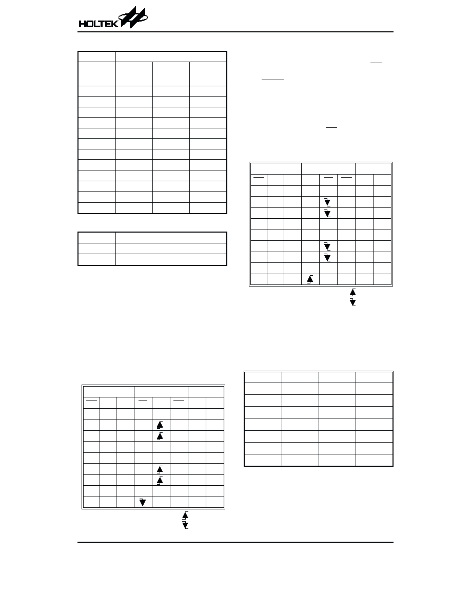
Timing Diagrams Pulse mode
·
Tone mode
HT9315 Series
Rev. 1.20
15
October 1, 2002
K E Y I N
P O
D T M .
T
I D P
- T
M
T
D B
T
D B
T
P D P
T
M
T
M
T
B
T
P D P
T
I D P
H i g h I m p e d a n c e
H K S
R
D 2
D 1
T
M
T
D B
T
I D P
- T
M
X 2
2 0 m s
2 0 m s
T
I D P
- T
M
X M U T E
D T M .
H i g h I m p e d a n c e
H K S
X M U T E
T
D B
T
I T P M
T
I T P M
T
T M I N
K E Y I N
R
D 1
T
I T P M
T
I T P M
P O
T
D B
T
D B
X 2
2 0 m s
2 0 m s
D 2
Dialing with pause key
·
Pulse mode
·
Tone mode
HT9315 Series
Rev. 1.20
16
October 1, 2002
K E Y I N
P O
D T M .
T
I D P
T
D B
T
P D P
H i g h I m p e d a n c e
H K S
D 3
D 2
D 1
T
M
T
P
+ T
P D P
P
X 2
2 0 m s
X M U T E
T
M
D T M .
H i g h I m p e d a n c e
T
D B
T
I T P M
K E Y I N
D 3
D 2
T
T M I N
T
I T P M
P
T
P
T
I T P M
D 1
P O
H K S
X M U T E
X 2
2 0 m s
Flash key operation
Pulse
®Tone operation
HT9315 Series
Rev. 1.20
17
October 1, 2002
H K S
K E Y I N
T
. P
T
.
H i g h I m p e d a n c e
T
D B
D T M .
P O
X M U T E
.
X 2
2 0 m s
T
I D P
+ T
P D P
P O
K E Y I N
D T M .
H i g h I m p e d a n c e
T
P D P
T
T M I N
T
D B
T
I T P M
T
I D P
T
P
T
D 1
D 2
D 3
* / T
X 2
2 0 m s
H K S
X M U T E
One-key redial operation
CLOCK & DOUT operation
HT9315 Series
Rev. 1.20
18
October 1, 2002
T
R P
( 1 s e c )
P O
T
B R K
( 1 . 2 s e c s )
T
I T P M
T
I T P M
H i g h I m p e d a n c e
T
I T P M
T
I T P M
K E Y I N
D T M .
D 1
D 2
R
T
D B
T
D B
T
D B
X 2
2 0 m s
H K S
X M U T E
P O
X M U T E
H K S
T
P D P
T
D B
T
B
T
M
H i g h I m p e d a n c e
D 1
K E Y I N
N o t e : D 1 = D 3 = 3
D 2 = 2
.
C L O C K
= 2 . 4 k H z
D a t a
X 2
C L O C K
D O U T
2 0 m s
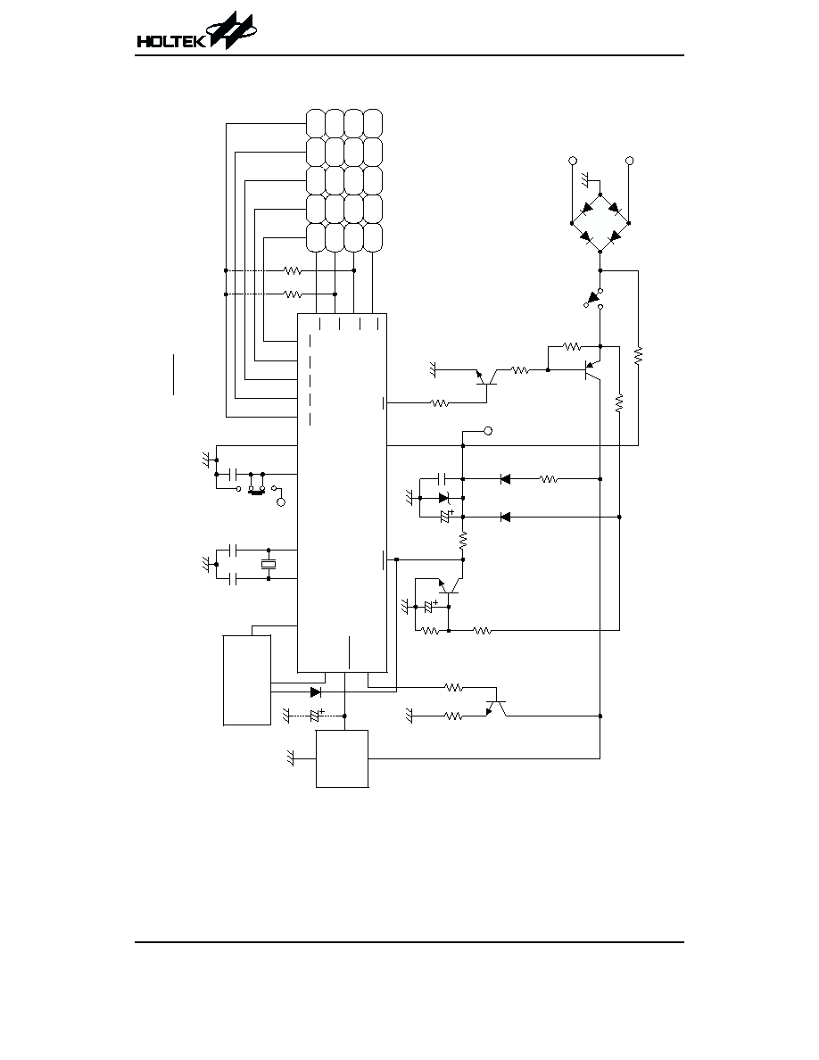
Application Circuits
Application circuit 1
HT9315 Series
Rev. 1.20
19
October 1, 2002
*
R
k
f
o
r
d
i
a
l
i
n
g
s
i
g
n
a
l
o
p
t
i
o
n
(
R
e
f
e
r
t
o
t
h
e
f
u
n
c
t
i
o
n
a
l
d
e
s
c
r
i
p
t
i
o
n
)
*
U
n
s
p
e
c
i
f
i
e
d
t
r
a
n
s
i
s
t
o
r
s
a
r
e
o
f
8
0
5
0
t
y
p
e
*
A
1
m
.
c
a
p
a
c
i
t
o
r
b
e
t
w
e
e
n
X
M
U
T
E
a
n
d
V
S
S
(
G
N
D
)
i
s
r
e
c
o
m
m
e
n
d
e
d
C
5
C
4
R
4
P
O
H
K
S
X
M
U
T
E
H
T
9
3
1
5
A
/
A
L
V
S
S
M
O
D
E
X
1
X
2
1
0
p
p
s
2
0
p
p
s
T
o
n
e
7
8
3
.
5
8
M
H
z
r
e
s
o
n
a
t
o
r
V
D
D
1
5
0
W
1
4
1
3
5
.
1
V
1
N
4
1
4
8
1
N
4
1
4
8
A
4
2
A
9
2
2
2
M
W
T
i
p
R
i
n
g
1
A
b
r
i
d
g
e
1
4
3
2
1
0
p
.
9
6
D
T
M
.
1
5
1
6
1
7
1
8
R
k
R
k
S
P
E
E
C
H
N
E
T
W
O
R
K
R
2
R
1
R
3
C
1
C
2
C
3
1
1
1
0
1
2
5
V
D
D
V
D
D
1
4
7
*
/
T
2
5
8
0
3
6
9
#
S
A
.
A
R
/
P
E
M
1
E
M
2
E
M
3
S
T
3
9
p
.
3
9
p
.
1
m
.
1
.
5
k
W
1
0
0
k
W
2
2
0
k
W
2
7
0
k
W
1
0
0
m
.
2
.
2
k
W
0
.
1
m
.
4
7
k
W
1
0
0
k
W
1
0
0
k
W
3
.
3
k
W
O
f
f
-
h
o
o
k
O
n
-
h
o
o
k
1
m
.
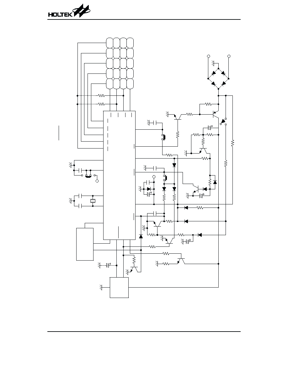
Application circuit 2
HT9315 Series
Rev. 1.20
20
October 1, 2002
*
R
k
f
o
r
d
i
a
l
i
n
g
s
i
g
n
a
l
o
p
t
i
o
n
(
R
e
f
e
r
t
o
t
h
e
f
u
n
c
t
i
o
n
a
l
d
e
s
c
r
i
p
t
i
o
n
)
*
U
n
s
p
e
c
i
f
i
e
d
t
r
a
n
s
i
s
t
o
r
s
a
r
e
o
f
8
0
5
0
t
y
p
e
*
A
1
m
.
c
a
p
a
c
i
t
o
r
b
e
t
w
e
e
n
X
M
U
T
E
a
n
d
V
S
S
(
G
N
D
)
i
s
r
e
c
o
m
m
e
n
d
e
d
C
5
H
K
S
1
5
0
W
5
.
1
V
H
o
l
d
1
N
4
1
4
8
1
N
4
1
4
8
1
N
4
1
4
8
1
N
4
1
4
8
x
4
1
m
.
1
6
V
1
N
4
1
4
8
H
a
n
d
-
f
r
e
e
A
4
2
1
0
m
.
5
0
V
A
9
2
2
2
M
W
T
i
p
R
i
n
g
1
A
b
r
i
d
g
e
C
4
R
4
X
M
U
T
E
V
S
S
M
O
D
E
X
1
X
2
V
D
D
1
0
p
p
s
2
0
p
p
s
T
o
n
e
8
3
.
5
8
M
H
z
r
e
s
o
n
a
t
o
r
H
D
O
1
7
1
6
1
2
9
2
5
4
3
1
0
p
.
1
0
7
D
T
M
.
H
.
O
1
8
1
9
2
0
2
1
R
k
R
k
R
2
R
1
R
3
C
1
C
2
C
3
1
5
H
.
I
1
1
2
2
1
H
D
I
V
D
D
1
3
1
4
S
P
E
E
C
H
N
E
T
W
O
R
K
P
O
6
V
D
D
1
4
7
*
/
T
2
5
8
0
3
6
9
#
S
A
.
A
R
/
P
E
M
1
E
M
2
E
M
3
S
T
3
9
p
.
3
9
p
.
1
.
5
k
W
1
m
.
1
0
0
k
W
4
7
k
W
2
7
0
k
W
2
2
0
k
W
2
.
2
k
W
0
.
1
m
.
1
0
0
m
.
0
.
1
m
.
0
.
1
m
.
2
2
k
W
2
2
k
W
3
3
0
k
W
1
0
0
k
W
2
2
0
k
W
1
0
0
k
W
2
2
0
k
W
1
0
k
W
3
3
k
W
4
7
k
W
0
.
0
2
m
.
3
.
3
k
W
1
0
0
k
W
O
f
f
-
h
o
o
k
O
n
-
h
o
o
k
1
m
.
H
T
9
3
1
5
B
/
B
L
Application circuit 3
HT9315 Series
Rev. 1.20
21
October 1, 2002
*
R
k
f
o
r
d
i
a
l
i
n
g
s
i
g
n
a
l
o
p
t
i
o
n
(
R
e
f
e
r
t
o
t
h
e
f
u
n
c
t
i
o
n
a
l
d
e
s
c
r
i
p
t
i
o
n
)
*
U
n
s
p
e
c
i
f
i
e
d
t
r
a
n
s
i
s
t
o
r
s
a
r
e
o
f
8
0
5
0
t
y
p
e
*
A
1
m
.
c
a
p
a
c
i
t
o
r
b
e
t
w
e
e
n
X
M
U
T
E
a
n
d
V
S
S
(
G
N
D
)
i
s
r
e
c
o
m
m
e
n
d
e
d
C
5
C
4
R
4
P
O
H
K
S
X
M
U
T
E
V
S
S
M
O
D
E
X
1
X
2
V
D
D
1
0
p
p
s
2
0
p
p
s
T
o
n
e
7
8
3
.
5
8
M
H
z
r
e
s
o
n
a
t
o
r
V
D
D
1
5
0
W
1
6
1
5
5
.
1
V
1
N
4
1
4
8
1
N
4
1
4
8
A
4
2
A
9
2
2
2
M
W
T
i
p
R
i
n
g
1
A
b
r
i
d
g
e
1
4
3
2
9
6
D
T
M
.
1
7
1
8
1
9
2
0
R
k
R
k
R
2
R
1
R
3
C
1
C
2
C
3
1
3
1
2
1
4
1 N 4 1 4 8
1
0
D
O
U
T
C
L
O
C
K
1
1
S
P
E
E
C
H
N
E
T
W
O
R
K
H
T
1
6
X
X
L
C
D
D
R
I
V
E
R
(
s
e
e
H
T
1
6
X
X
d
a
t
a
)
5
1
0
p
.
V
D
D
1
4
7
*
/
T
2
5
8
0
3
6
9
#
S
A
.
A
R
/
P
E
M
1
E
M
2
E
M
3
S
T
3
9
p
.
3
9
p
.
1
m
.
1
.
5
k
W
1
0
0
k
W
2
2
0
k
W
2
7
0
k
W
1
0
0
m
.
0
.
1
m
.
2
.
2
k
W
4
7
k
W
1
0
0
k
W
3
.
3
k
W
1
0
0
k
W
O
f
f
-
h
o
o
k
O
n
-
h
o
o
k
1
m
.
H
T
9
3
1
5
C
/
C
L
Application circuit 4
HT9315 Series
Rev. 1.20
22
October 1, 2002
*
R
k
f
o
r
d
i
a
l
i
n
g
s
i
g
n
a
l
o
p
t
i
o
n
(
R
e
f
e
r
t
o
t
h
e
f
u
n
c
t
i
o
n
a
l
d
e
s
c
r
i
p
t
i
o
n
)
*
U
n
s
p
e
c
i
f
i
e
d
t
r
a
n
s
i
s
t
o
r
s
a
r
e
o
f
8
0
5
0
t
y
p
e
*
A
1
m
.
c
a
p
a
c
i
t
o
r
b
e
t
w
e
e
n
X
M
U
T
E
a
n
d
V
S
S
(
G
N
D
)
i
s
r
e
c
o
m
m
e
n
d
e
d
1
5
0
W
5
.
1
V
H
o
l
d
1
N
4
1
4
8
1
N
4
1
4
8
1
N
4
1
4
8
1
N
4
1
4
8
x
4
1
m
.
1
6
V
1
N
4
1
4
8
2
2
0
k
W
H
a
n
d
-
f
r
e
e
A
4
2
1
0
m
.
5
0
V
A
9
2
2
2
M
W
T
i
p
R
i
n
g
1
A
b
r
i
d
g
e
C
4
R
4
P
O
X
M
U
T
E
V
S
S
M
O
D
E
X
1
X
2
1
0
p
p
s
2
0
p
p
s
T
o
n
e
8
3
.
5
8
M
H
z
r
e
s
o
n
a
t
o
r
H
D
O
1
9
1
8
1
4
9
1
2
2
5
4
3
1
0
p
.
1
0
7
D
T
M
.
H
.
O
2
0
2
1
2
2
2
3
R
k
R
k
1
m
.
R
2
R
1
R
3
C
1
C
2
C
3
1
7
H
.
I
1
1
2
4
1
H
D
I
V
D
D
1
5
1
6
S
P
E
E
C
H
N
E
T
W
O
R
K
C
L
O
C
K
1
3
D
O
U
T
H
T
1
6
X
X
L
C
D
D
R
I
V
E
R
(
s
e
e
H
T
1
6
X
X
d
a
t
a
)
H
K
S
1
N
4
1
4
8
C
5
6
V
D
D
V
D
D
1
4
7
*
/
T
2
5
8
0
3
6
9
#
S
A
.
A
R
/
P
E
M
1
E
M
2
E
M
3
S
T
3
9
p
.
3
9
p
.
1
m
.
1
.
5
k
W
4
7
k
W
4
7
k
W
1
0
0
k
W
2
7
0
k
W
2
2
0
k
W
2
.
2
k
W
0
.
1
m
.
1
0
0
m
.
2
2
k
W
1
0
0
k
W
3
3
0
k
W
0
.
1
m
.
0
.
1
m
.
2
2
0
k
W
1
0
0
k
W
3
3
k
W
4
7
k
W
1
0
k
W
0
.
0
2
m
.
3
.
3
k
W
1
0
0
k
W
O
f
f
-
h
o
o
k
O
n
-
h
o
o
k
2
2
k
W
H
T
9
3
1
5
D
/
D
L

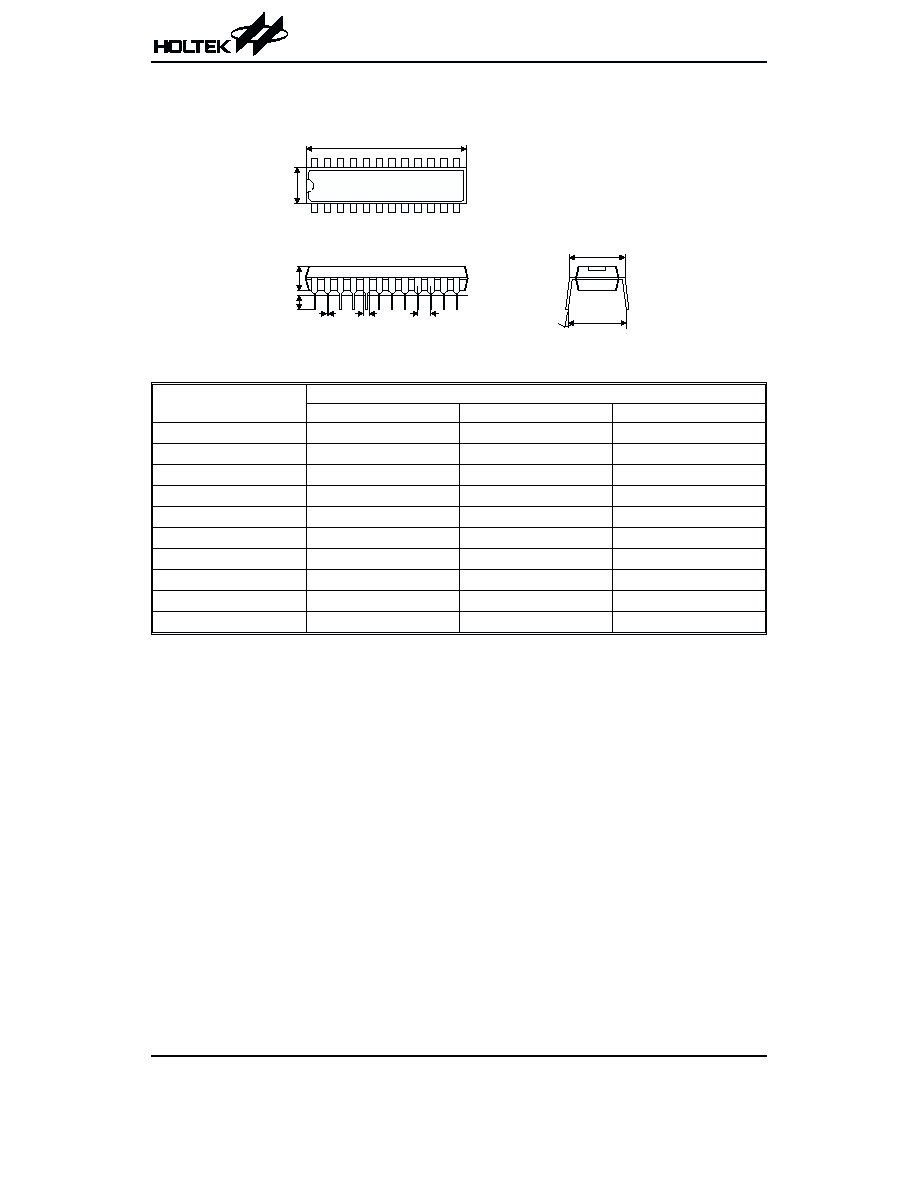
Package Information
18-pin DIP (300mil) outline dimensions
Symbol
Dimensions in mil
Min.
Nom.
Max.
A
895
¾
915
B
240
¾
260
C
125
¾
135
D
125
¾
145
E
16
¾
20
F
50
¾
70
G
¾
100
¾
H
295
¾
315
I
335
¾
375
a
0
°
¾
15
°
HT9315 Series
Rev. 1.20
23
October 1, 2002
1 8
1
1 0
9
a
A
B
C
D
E
.
G
H
I
20-pin DIP (300mil) outline dimensions
Symbol
Dimensions in mil
Min.
Nom.
Max.
A
1020
¾
1045
B
240
¾
260
C
125
¾
135
D
125
¾
145
E
16
¾
20
F
50
¾
70
G
¾
100
¾
H
295
¾
315
I
335
¾
375
a
0
°
¾
15
°
HT9315 Series
Rev. 1.20
24
October 1, 2002
2 0
1
1 1
1 0
a
A
B
C
D
E
.
G
H
I
22-pin SKDIP (300mil) outline dimensions
Symbol
Dimensions in mil
Min.
Nom.
Max.
A
1085
¾
1105
B
253
¾
263
C
125
¾
135
D
125
¾
145
E
16
¾
20
F
50
¾
70
G
¾
100
¾
H
295
¾
315
I
330
¾
375
a
0
°
¾
15
°
HT9315 Series
Rev. 1.20
25
October 1, 2002
2 2
1
1 2
1 1
a
A
B
C
D
E
.
G
H
I
24-pin SKDIP (300mil) outline dimensions
Symbol
Dimensions in mil
Min.
Nom.
Max.
A
1235
¾
1265
B
255
¾
265
C
125
¾
135
D
125
¾
145
E
16
¾
20
F
50
¾
70
G
¾
100
¾
H
295
¾
315
I
345
¾
360
a
0
°
¾
15
°
HT9315 Series
Rev. 1.20
26
October 1, 2002
2 4
1
1 3
1 2
a
A
B
C
D
E
.
G
H
I

HT9315 Series
Rev. 1.20
27
October 1, 2002
Copyright
Ó 2002 by HOLTEK SEMICONDUCTOR INC.
The information appearing in this Data Sheet is believed to be accurate at the time of publication. However, Holtek as-
sumes no responsibility arising from the use of the specifications described. The applications mentioned herein are used
solely for the purpose of illustration and Holtek makes no warranty or representation that such applications will be suitable
without further modification, nor recommends the use of its products for application that may present a risk to human life
due to malfunction or otherwise. Holtek
¢s products are not authorized for use as critical components in life support devices
or systems. Holtek reserves the right to alter its products without prior notification. For the most up-to-date information,
please visit our web site at http://www.holtek.com.tw.
Holtek Semiconductor Inc. (Headquarters)
No.3, Creation Rd. II, Science Park, Hsinchu, Taiwan
Tel: 886-3-563-1999
Fax: 886-3-563-1189
http://www.holtek.com.tw
Holtek Semiconductor Inc. (Taipei Sales Office)
4F-2, No. 3-2, YuanQu St., Nankang Software Park, Taipei 115, Taiwan
Tel: 886-2-2655-7070
Fax: 886-2-2655-7373
Fax: 886-2-2655-7383 (International sales hotline)
Holtek Semiconductor Inc. (Shanghai Sales Office)
7th Floor, Building 2, No.889, Yi Shan Rd., Shanghai, China 200233
Tel: 021-6485-5560
Fax: 021-6485-0313
http://www.holtek.com.cn
Holtek Semiconductor Inc. (Shenzhen Sales Office)
43F, SEG Plaza, Shen Nan Zhong Road, Shenzhen, China 518031
Tel: 0755-8346
-
5589
Fax: 0755-8346
-
5590
ISDN: 0755-8346
-
5591
Holtek Semiconductor Inc. (Beijing Sales Office)
Suite 1721, Jinyu Tower, A129 West Xuan Wu Men Street, Xicheng District, Beijing, China 100031
Tel: 010-6641
-
0030, 6641
-
7751, 6641
-
7752
Fax: 010-6641
-
0125
Holmate Semiconductor, Inc. (North America Sales Office)
46712 Fremont Blvd., Fremont, CA 94538
Tel: 510-252-9880
Fax: 510-252-9885
http://www.holmate.com
Document Outline
- þÿ
- þÿ
- þÿ
- þÿ
- þÿ
- þÿ
- þÿ
- þÿ
- þÿ
- þÿ
- þÿ
- þÿ
- þÿ
- þÿ
- þÿ