 | –≠–ª–µ–∫—Ç—Ä–æ–Ω–Ω—ã–π –∫–æ–º–ø–æ–Ω–µ–Ω—Ç: HT93214 | –°–∫–∞—á–∞—Ç—å:  PDF PDF  ZIP ZIP |
Document Outline
- ˛ˇ
- ˛ˇ
- ˛ˇ
- ˛ˇ
- ˛ˇ
- ˛ˇ
- ˛ˇ
- ˛ˇ
- ˛ˇ
- ˛ˇ
- ˛ˇ
- ˛ˇ
- ˛ˇ
- ˛ˇ

HT93214 Series
1-memory Tone/Pulse Dialer
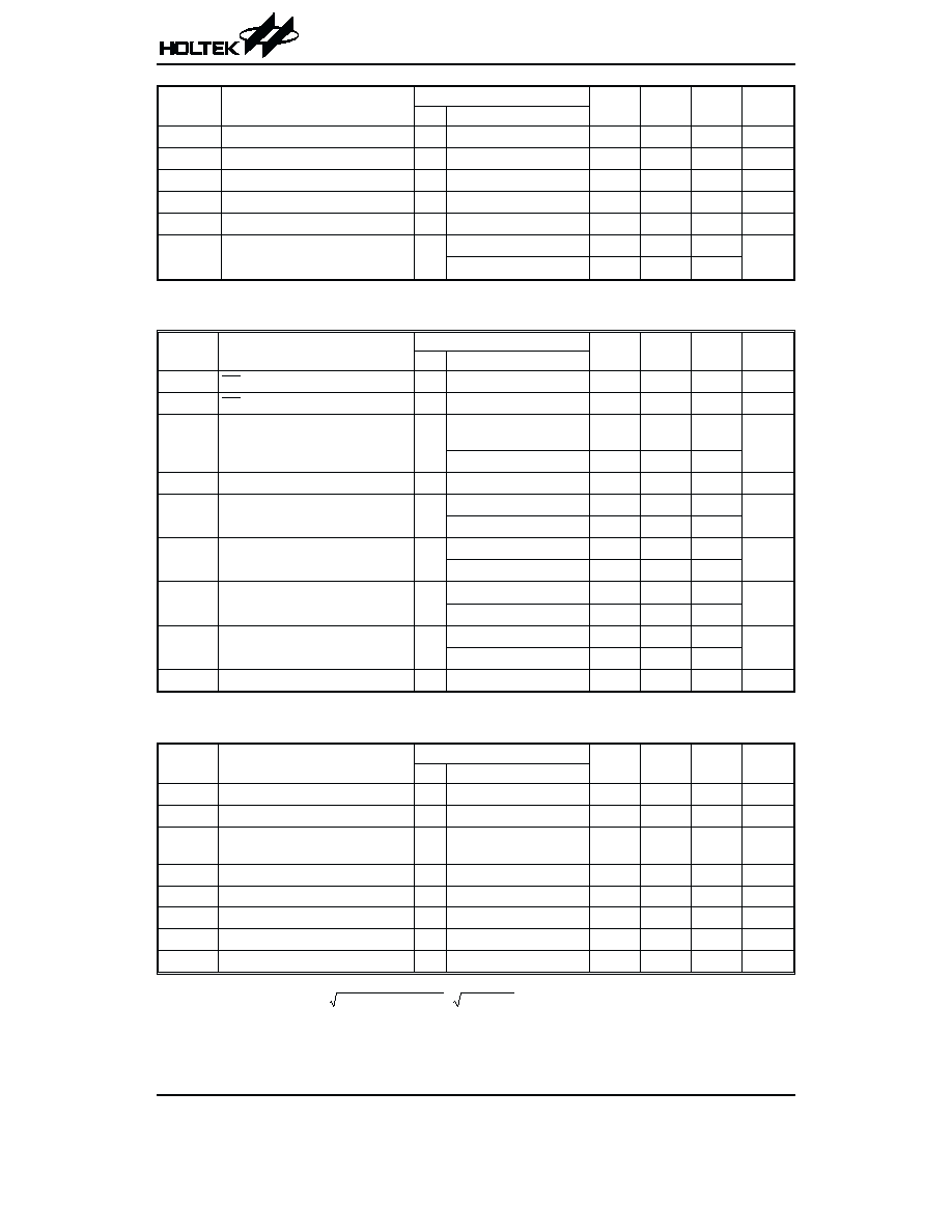
Selection Table
HT93214 series
Function
Part No.
Hand-
Free
Key
Tone
Flash
Flash
Time
(ms)
Pulse
No.
Tone
Duration
(ms)
Inter
Tone
Pause (ms)
PPS
M/B
PKG
DIP
300mil
HT93214A
Control
300/600
N
94
96
10/20
1/2
16
HT93214B
÷
Control
300/600
N
94
96
10/20
1/2
18
HT93214AT
÷
Control
300/600
N
94
96
10/20
1/2
18
Rev. 1.10
1
October 2, 2002
Features
∑
Operating Voltage: 2.0V~5.5V
∑
Low standby current
∑
Low memory retention current: 0.1
mA (Typ.)
∑
Tone/Pulse switchable
∑
32 (pulse)/31 (tone) digits for redialing
∑
Pause and P
Æ T key for PBX
∑
4
¥4 keyboard matrix
∑
3.58MHz crystal or ceramic resonator
∑
Hand-free control
∑
Pause, P
Æ T can be saved for redialing
∑
One-key redialing
∑
Keytone output
∑
Pause time: 2.2s
∑
Cascadable manual dialing after redialing
∑
Calibrated DTMF timing for redialing
∑
HT93214A: 16-pin DIP package
HT93214B/AT: 18-pin DIP package
General Description
The HT93214 are dialer series designed for low cost
telephone set applications with expandable features
such as Lock function, keytone and LCD display inter-
face. With a 4
¥4 keyboard, it performs normal
tone/pulse switchable dialing, and provides one-key
redialing function with a 32-digit memory for speed dial-
ing. An on-chip oscillator is built-in to work with an exter-
nal 3.58Mhz crystal or ceramic resonator for accurate
timing. The HT93214 provides 300ms (F1 key) and
600ms (F2 key) of flash time; Tone dialing and 10pps,
20pps selection with 1/2 M/B ratio for pulse dialing.
Patent Number: 86474, 84545(R.O.C)

Block Diagram
Pin Assignment
Keyboard Information
HT93214 Series
Rev. 1.10
2
October 2, 2002
1 6
1 5
1 4
1 3
1 2
1 1
1 0
9
1
2
3
4
5
6
7
8
1 8
1 7
1 6
1 5
1 4
1 3
1 2
1 1
1 0
1
2
3
4
5
6
7
8
9
H K S
M O D E
X 1
X 2
V S S
V D D
D T M .
X M U T E
R 4
R 3
R 2
R 1
C 3
C 2
C 1
P O
H . O
H K S
M O D E
X 1
X 2
V S S
V D D
D T M .
X M U T E
R 4
R 3
R 2
R 1
C 3
C 2
C 1
P O
H . I
1 8
1 7
1 6
1 5
1 4
1 3
1 2
1 1
1 0
1
2
3
4
5
6
7
8
9
H K S
M O D E
X 1
X 2
V S S
V D D
D T M .
X M U T E
M O D E O
R 4
R 3
R 2
R 1
C 3
C 2
C 1
P O
K T
H T 9 3 2 1 4 A
1 6 D I P - A
H T 9 3 2 1 4 B
1 8 D I P - A
H T 9 3 2 1 4 A T
1 8 D I P - A
C 1
R 1
P O
K e y
C o l u m n
. S M
K e y
. u n c t i o n
E n c o d e r
E n c o d e r
C o n t r o l
W R M
C o u n t e r
A D D R L
K e y R o w
S R A M
D e b o u n c e
D i v i d e r
C l o c k
G e n e r a t o r
M / B
. l a s h / M o d e
T i m e r
C h e c k
T o n e
E n c o d e r
C o n v e r t e r
H .
T o n e
O u t
P u l s e
O u t
X 1
X 2
D T M .
H . I
M O D E
M O D E O
X M U T E
C 3
R 4
C l o c k
C o n t r o l
K e y t o n e
G e n e r a t o r
H K S
H . O
K T
2
5
8
0
3
6
9
#
. 1
. 2
P
R
C 1
C 2
C 3
R 4
R 3
R 2
R 1
1
4
7
* / T
H K S

Pin Description
Pin Name
I/O
Internal
Connection
Description
C1~C3
R1~R4
I/O
CMOS
I/O
These pins along with the HKS form a 4
¥4 keyboard matrix which can perform key-
board input detection. When on-hook (HKS=high) all the pins are set high. While
off-hook the column group (C1~C3) is set low and the row group (R1~R4) remains
high for input detection.
Pressing a key connects a single row to a single column HKS and actuates the sys-
tem oscillator that results in a dialing signal output. If more than two keys are
pressed at the same time, no response occurs. The key-in debounce time is 20ms.
X1
I
OSC
The system oscillator consists of an inverter, a bias resistor and the necessary load
capacitor on chip. Connecting a standard 3.579545MHz crystal or ceramic resona-
tor to the X1 and X2 terminals can implement the oscillator function. The oscillator is
turned off in the standby mode, and is actuated whenever a keyboard entry is de-
tected.
X2
O
XMUTE
O
NMOS
Open Drain
NMOS open drain structure pulled to VSS during dialing signal transmission. Other-
wise, it is an open circuit. This pin is used to mute the speech circuit when transmit-
ting the dial signal.
HKS
I
CMOS
This pin is used to monitor the status of the hook-switch and its combination with
HFI can control the PO pin output to make or break the line.
HKS=VDD: On-hook state (PO=low). Except for HFI (hand-free control input), other
functions are all disabled.
HKS=VSS: Off-hook state (PO=high). The chip is in the stand-by mode and ready
to receive the key input.
PO
O
NMOS
NMOS open drain output structure, which by receiving the HKS and HFO signals,
control the dialer so as to connect or disconnect the telephone line.
PO is pulled to VSS when HKS is high (on-hook) and HFO is low.
PO is an open circuit which make the line connection when HKS is low (off-hook) or
HFO is high.
During the off-hook state, this pin also outputs the dialing pulse train in pulse mode
dialing. While in the tone mode, this pin is always an open circuit.
MODE
I/O
CMOS
This is a tri-state input/output pin, used for dialing mode selection, either Tone
mode or Pulse mode, 10pps/20pps
MODE=VDD: Pulse, 10pps, M/B=1/2
MODE=Floating: Pulse, 20pps, M/B=1/2
MODE=VSS: Tone.
The MODE selection is checked each time a key input is received.
DTMF
O
CMOS
This pin is active only when the chip transmits tone dialing signals. Otherwise, it al-
ways outputs a low. The pin outputs tone signals to drive the external transmitter
amplifier circuit. The load resistor (to V
SS
) should not be less than 5k
W and any DC
load connected to V
DD
is not allowed.
KT
O
NMOS
NMOS open drain structure for keytone output. It outputs 34ms of 600Hz tone burst
when any key is pressed in the pulse mode or when a function key is pressed in the
tone mode.
HFI
I
CMOS
Pulled-high, this pin is a Schmitt trigger input structure. Active low. Applying a nega-
tive going pulse to HFI can toggle the HFO once and hence control the hand-free
function. The pull-high resistance of HFI is about 200k
W typ. An external RC net-
work is recommended for input debouncing.
HFO
O
CMOS
The HFO pin is a CMOS output structure. Its output is toggle- controlled by a nega-
tive transition on HFI pin. When HFO is high, the hand-free function is enabled and
PO outputs a high to connect the line.
The hand-free function can be released by an on-off-hook operation or by another
HFI input. Refer to the functional description for the hand-free functional operation.
VDD
æ
æ
Positive power supply, 2.0V~5.5V for normal operation
VSS
æ
æ
Negative power supply, ground
MODEO
O
NMOS
NMOS open drain output pin pulled to VSS during tone output and is an open circuit
during pulse output.
HT93214 Series
Rev. 1.10
3
October 2, 2002

Approximate internal connection circuits
Absolute Maximum Ratings
Supply Voltage ............................................
-0.3V to 6V
Storage Temperature ............................
-50∞C to 125∞C
Input Voltage..............................V
SS
-0.3V to V
DD
+0.3V
Operating Temperature...........................
-20∞C to 75∞C
Note: These are stress ratings only. Stresses exceeding the range specified under
≤Absolute Maximum Ratings≤ may
cause substantial damage to the device. Functional operation of this device at other conditions beyond those
listed in the specification is not implied and prolonged exposure to extreme conditions may affect device reliabil-
ity.
Electrical Characteristics
F
OSC
=3.5795MHz, Ta=25
∞C
Symbol
Parameter
Test Conditions
Min.
Typ.
Max.
Unit
V
DD
Conditions
V
DD
Operating Voltage
æ
æ
2
æ
5.5
V
I
DD
Operating Current
2.5V
Pulse
Off-hook
Keypad entry
æ
0.2
1
mA
Tone
æ
0.6
2
mA
I
STB
Standby Current
1V
On-hook, no load
No entry
æ
æ
1
mA
V
R
Memory Retention Voltage
æ
æ
1
æ
5
V
I
R
Memory Retention Current
1V
On-hook
æ
0.1
0.2
mA
V
IL
Input Low Voltage
æ
æ
V
SS
æ
0.2V
DD
V
V
IH
Input High Voltage
æ
æ
0.8V
DD
æ
V
DD
V
I
XMO
XMUTE Leakage Voltage
æ
V
XMUTE
=12V
No entry
æ
æ
1
mA
I
OLXM
XMUTE Sink Current
2.5V V
XMUTE
=0.5V
1
æ
æ
mA
I
HKS
HKS Pin Input Current
2.5V V
HKS
=2.5V
æ
0.1
mA
R
HFI
HFI Pull- High Resistance
2.5V V
HFI
=0V
æ
200
æ
k
W
I
OH1
Keypad Pin Source Current
2.5V V
OH
=0V
-4
æ
-40
mA
I
OL1
Keypad Pin Sink Current
2.5V V
OL
=2.5V
200
400
æ
mA
I
OH2
HFO Pin Source Current
2.5V V
OH
=2V
-1
æ
æ
mA
I
OL2
HFO Pin Sink Current
2.5V V
OL
=0.5V
1
æ
æ
mA
I
OL3
MODEO Sink Current
2.5V V
OL
=0.5V
0.6
3.5
æ
mA
HT93214 Series
Rev. 1.10
4
October 2, 2002
N M O S O U T
V
D D
C M O S I N / O U T
C M O S O U T
C M O S I N
P u l l - L o w
C M O S I N
P u l l - H i g h
C M O S I N
O S C I L L A T O R
X 1
X 2
E N
1 0 M
2 0 P
1 0 P
V
D D
Symbol
Parameter
Test Conditions
Min.
Typ.
Max.
Unit
V
DD
Conditions
T
FP
Pause Time After Flash
2.5V
æ
æ
800
æ
ms
T
RP
One-key Redialing Pause Time
2.5V
æ
æ
800
æ
ms
F
OSC
System Frequency
æ
æ
æ
3.58
æ
MHz
T
DB
Key-in Debounce Time
2.5V
æ
æ
20
æ
ms
T
BRK
Break Time For One-key Redialing 2.5V
æ
æ
2.2
æ
s
T
HKDL
Off-hook Delay Time
2.5V
10pps
æ
800
æ
ms
20pps
æ
500
æ
Pulse Mode Electrical Characteristics
F
OSC
=3.5795MHz, Ta=25
∞C
Symbol
Parameter
Test Conditions
Min.
Typ.
Max.
Unit
V
DD
Conditions
I
POH
PO Output Source Current
2.5V V
OH
=2V
-0.2
æ
æ
mA
I
POL
PO Output Sink Current
2.5V V
OL
=0.5V
0.2
0.6
æ
mA
P
R
Pulse Rate
æ
MODE pin is
connected to V
DD
æ
10
æ
pps
MODE pin is opened
æ
20
æ
M/B
Make/Break Ratio
æ
æ
æ
33:66
æ
%
T
PDP
Pre-digit-pause Time
æ
M/B=33:66 (10 pps)
æ
33
æ
ms
M/B=33:66 (20 pps)
æ
17
æ
T
IDP
Inter-digit-pause Time
æ
10 pps
æ
800
æ
ms
20 pps
æ
500
æ
T
M
Pulse Make Duration
æ
10 pps, M/B=1/2
æ
33.3
æ
ms
20 pps, M/B=1/2
æ
16.7
æ
T
B
Pulse Break Duration
æ
10 pps, M/B=1/2
æ
66.6
æ
ms
20 pps, M/B=1/2
æ
33.3
æ
T
P
Pause Time
æ
æ
æ
2.2
æ
s
Tone Mode Electrical Characteristics
F
OSC
=3.5795MHz, Ta=25
∞C
Symbol
Parameter
Test Conditions
Min.
Typ.
Max.
Unit
V
DD
Conditions
V
TDC
DTMF Output DC Level
æ No load
0.45V
DD
æ
0.7V
DD
V
I
TOL
DTMF Sink Current
2.5V V
DTMF
=0.5V
0.1
æ
æ
mA
V
TAC
DTMF Output AC Level
æ
Row group,
R
L
=5k
W
0.12
0.155
0.18
Vrms
R
L
DTMF Output Load
2.5V THD
£-23dB
5
æ
æ
k
W
A
CR
Column Pre-emphasis
2.5V Row group=0dB
1
2
3
dB
THD
Tone Signal Distortion
2.5V R
L
=5k
W
æ
-30
-23
dB
T
TMIN
Minimum Tone Duration
æ Auto-redial
æ
94
æ
ms
T
ITPM
Minimum Inter-Tone Pause
æ Auto-redial
æ
96
æ
ms
THD (Distortion) (dB) = 20 log ( V1
V2
.... Vn
2
2
2
+
+ +
/
Vi
Vh
2
2
+
)
Vi, Vh: Row group and column group signals
V1, V2, ... Vn: Harmonic signals (BW=300Hz~3500Hz)
HT93214 Series
Rev. 1.10
5
October 2, 2002