 | ÐлекÑÑоннÑй компоненÑ: HT95AXXX | СкаÑаÑÑ:  PDF PDF  ZIP ZIP |
Äîêóìåíòàöèÿ è îïèñàíèÿ www.docs.chipfind.ru

HT95AXXX
I/O Type Phone 8-Bit MCU
Rev. 1.20
1
May 26, 2004
Features
·
Provide MASK type and OTP type version
·
Operating voltage range: 2.4V~5.5V
·
Program ROM
-
HT95A400/40P: 16K
´16 bits
-
HT95A300/30P: 8K
´16 bits
-
HT95A200/20P: 4K
´16 bits
-
HT95A100/10P: 4K
´16 bits
·
Data RAM
-
HT95A400/40P: 2880
´8 bits
-
HT95A300/30P: 2112
´8 bits
-
HT95A200/20P: 1152
´8 bits
-
HT95A100/10P: 384
´8 bits
·
Bidirectional I/O lines
-
HT95A400/40P: 44 I/O lines
-
HT95A300/30P: 28 I/O lines
-
HT95A200/20P: 28 I/O lines
-
HT95A100/10P: 20 I/O lines
·
16-bit table read instructions
·
Subroutine nesting
-
HT95A400/40P: 12 levels
-
HT95A300/30P: 8 levels
-
HT95A200/20P: 8 levels
-
HT95A100/10P: 4 levels
·
Timer
-
Two 16-bit programmable Timer/Event Counter
-
Real time clock (RTC)
-
Watchdog Timer (WDT)
·
Programmable frequency divider (PFD)
Supported for HT95A400/40P, HT95A300/30P,
HT95A200/20P
·
Dual system clock: 32768Hz, 3.58MHz
·
Four operating modes: Idle mode, Sleep mode,
Green mode and Normal mode
·
Up to 1.117
ms instruction cycle with 3.58MHz system
clock
·
All instructions in one or two machine cycles
·
Built-in 3.58MHz DTMF Generator
·
Built-in dialer I/O
·
HT95A400/40P: 64-pin QFP package
HT95A300/40P: 48-pin SSOP package
HT95A200/20P: 48-pin SSOP package
HT95A100/10P: 28-pin SOP package
Applications
·
Cordless Phone
·
Fax and answering machines
·
Other communication system
General Description
The HT95AXXX family MCU are 8-bit high performance
RISC-like microcontrollers with built-in DTMF generator
and dialer I/O which provide MCU dialer implementation
or system control features for telecom product applica-
tions. The phone controller has a built-in program ROM,
data RAM and I/O lines for high end products design. In
addition, for power management purpose, it has a
built-in frequency up conversion circuit (32768Hz to
3.58MHz) which provides dual system clock and four
types of operation modes. For example, it can operate
with low speed system clock rate of 32768Hz in green
mode with little power consumption. It can also operate
with high speed system clock rate of 3.58MHz in normal
mode for high performance operation. To ensure
smooth dialer function and to avoid MCU shut-down in
extreme low voltage situation, the dialer I/O circuit is
built-in to generate hardware dialer signals such as
on-hook, hold-line and hand-free. Built-in real time clock
and programmable frequency divider are provided for
additional fancy features in product developments. The
device is best suited for phone products that comply
with versatile dialer specification requirements of differ-
ent areas or countries.
Selection Table
Part No.
Operating
Voltage
Program
Memory
Data
Memory
Normal
I/O
Dialer
I/O
LCD
Timer
Stack
External
Interrupt
DTMF
Generator
FSK
Receiver
Package
HT95A100
HT95A10P
2.4V~5.5V
4K
´16
384
´8
20
6
¾
16-bit
´2
4
3
Ö
¾
28SOP
HT95A200
HT95A20P
2.4V~5.5V
4K
´16
1152
´8
28
8
¾
16-bit
´2
8
4
Ö
¾
48SSOP
HT95A300
HT95A30P
2.4V~5.5V
8K
´16
2112
´8
28
8
¾
16-bit
´2
8
4
Ö
¾
48SSOP
HT95A400
HT95A40P
2.4V~5.5V
16K
´16
2880
´8
44
8
¾
16-bit
´2
12
4
Ö
¾
64QFP
HT95L000
HT95L00P
2.4V~5.5V
4K
´16
384
´8
14~18
6
12
´8~16´8
16-bit
´2
4
3
Ö
¾
56SSOP
HT95L100
HT95L10P
2.4V~5.5V
4K
´16
1152
´8
16~20
8
16
´8~20´8
16-bit
´2
8
4
Ö
¾
64QFP
HT95L200
HT95L20P
2.4V~5.5V
8K
´16
1152
´8
20~28
8
24
´8~24´16
16-bit
´2
8
4
Ö
¾
100QFP
HT95L300
HT95L30P
2.4V~5.5V
8K
´16
2112
´8
16~28
8
36
´16~48´16 16-bit´2
8
4
Ö
¾
100QFP
HT95L400
HT95L40P
2.4V~5.5V
16K
´16
2880
´8
28~40
8
36
´16~48´16 16-bit´2
12
4
Ö
¾
128QFP
HT95C200
HT95C20P
2.4V~5.5V
8K
´16
1152
´8
20~28
8
24
´8~24´16
16-bit
´2
8
4
Ö
Ö
128QFP
HT95C300
HT95C30P
2.4V~5.5V
8K
´16
2112
´8
16~28
8
36
´16~48´16 16-bit´2
8
4
Ö
Ö
128QFP
HT95C400
HT95C40P
2.4V~5.5V
16K
´16
2880
´8
28~40
8
36
´16~48´16 16-bit´2
12
4
Ö
Ö
128QFP
Note: Part numbers suffixed with
²P² are OTP devices, all others are mask version devices.
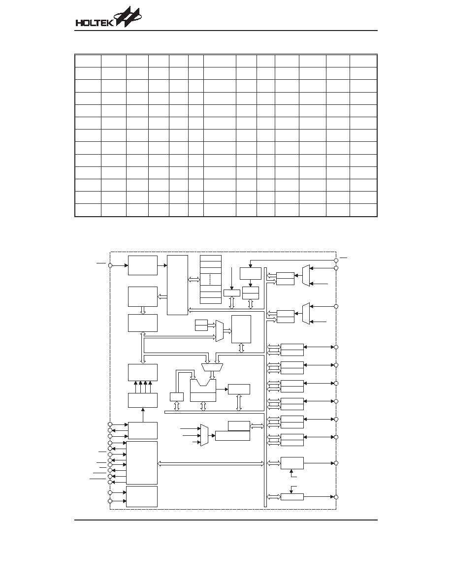
Block Diagram (HT95A400/40P)
HT95AXXX
Rev. 1.20
2
May 26, 2004
S T A C K 1 1
S T A C K 1 0
P r o g r a m
C o u n t e r
P r o g r a m
R O M
I n s t r u c t i o n
R e g i s t e r
I n s t r u c t i o n
D e c o d e r
T i m i n g
G e n e r a t o r
I N T C 1
I n t e r r u p t
C i r c u i t
M
U
X
M U X
D A T A
M e m o r y
A L U
S h i f t e r
S T A T U S
A C C
S T A C K 9
S T A C K 0
S T A C K 1
S T A C K 2
M P 1
M P 0
P o w e r D o w n
D e t e c t o r &
R e s e t C i r c u i t
I N T C 0
R T C
3 2 7 6 8 H z
O S C C i r c u i t
M
U
X
W D T S
W D T P r e s c a l e r
3 2 7 6 8 H z
S y s t e m C l o c k / 4
W D T O S C
T M R 1 C
T M R 1
M
U
X
3 2 7 6 8 H z
T M R 0 C
T M R 0
M
U
X
S y s t e m c l o c k / 4
P A
P A C
P F D
T M R 1
T M R 0
P A 0 ~ P A 7
M U S I C
R E S
X 1
X 2
X C
3 2 7 6 8 H z
o r 3 . 5 8 M H z / 4
P o w e r
S u p p l y
V D D
V S S
D i a l e r I / O
H F I
H F O
H D I
H D O
H K S
P O
D N P O
X M U T E
D T M F
G e n e r a t o r
D T M F
3 . 5 8 M H z
I N T
P B
P B C
P B 0 ~ P B 7
P D
P D C
P D 0 ~ P D 7
P E
P E C
P E 0 ~ P E 7
P F
P F C
P F 0 ~ P F 7
P G
P G C
P G 0 ~ P G 3
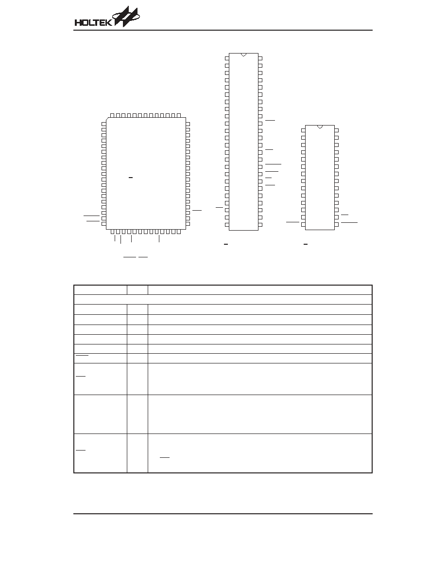
Pin Assignment
Note:
The following pads for the HT95A100/10P are not bonded to the package.
PD2, PD3, HKS, PO, HFI, HFO
Pin Description
Pin Name
I/O
Description
CPU
VDD
¾
Positive power supply
VSS
¾
Negative power supply, ground
X1
I
A 32768Hz crystal (or resonator) should be connected to this pin and X2.
X2
O
A 32768Hz crystal (or resonator) should be connected to this pin and X1.
XC
I
External low pass filter used for frequency up conversion circuit.
RES
I
Schmitt trigger reset input, active low.
INT
I
Supported for HT95A400/40P, HT95A300/30P, HT95A200/20P
Schmitt trigger input for external interrupt.
No internal pull-high resistor.
Edge trigger activated on a falling edge.
TMR0
I
Supported for HT95A400/40P, HT95A300/30P, HT95A200/20P
Schmitt trigger input for Timer/Event Counter 0.
No internal pull-high resistor.
Activated on falling or rising transition edge, selected by software.
Activated on a falling or rising transition edge, selected by software.
INT/TMR0
I
Supported for HT95A100/10P
Schmitt trigger input for external interrupt or Timer/Event Counter 0.
No internal pull-high resistor.
For INT: Edge trigger activated on a falling edge.
For TMR0: Activated on a falling or rising transition edge, selected by software.
HT95AXXX
Rev. 1.20
3
May 26, 2004
4 8
4 7
4 6
4 5
4 4
4 3
4 2
4 1
4 0
3 9
3 8
3 7
3 6
3 5
3 4
3 3
3 2
3 1
3 0
2 9
2 8
2 7
2 6
2 5
1
2
3
4
5
6
7
8
9
1 0
1 1
1 2
1 3
1 4
1 5
1 6
1 7
1 8
1 9
2 0
2 1
2 2
2 3
2 4
P A 3
P A 2
P A 1
P A 0
P B 7
P B 6
P B 5
P B 4
V S S
P B 3
P B 2
P B 1
P B 0
P D 7
P D 6
P D 5
P D 4
P D 3
P D 2
P D 1
P D 0
I N T
T M R 0
T M R 1
P A 4
P A 5
P A 6
P A 7
X 2
X 1
X C
N C
V D D
R E S
D T M F
H F I
H F O
H D I
H D O
X M U T E
D N P O
P O
H K S
P E 3
P E 2
P E 1
P E 0
M U S I C
H T 9 5 A 3 0 0 / 3 0 P / 2 0 0 / 2 0 P
4 8 S S O P - A
2 8
2 7
2 6
2 5
2 4
2 3
2 2
2 1
2 0
1 9
1 8
1 7
1 6
1 5
1
2
3
4
5
6
7
8
9
1 0
1 1
1 2
1 3
1 4
H T 9 5 A 1 0 0 / 1 0 P
2 8 S O P - A
P A 3
P A 2
P A 1
P A 0
P B 7
P B 6
P B 5
P B 4
P B 3
P B 2
P B 1
P B 0
V S S
D N P O
P A 4
P A 5
P A 6
P A 7
D T M F
P D 0
P D 1
X 2
X 1
X C
V D D
R E S
I N T / T M R 0
X M U T E
1
2
3
4
5
6
7
8
9
1 0
1 1
1 2
1 3
1 4
1 5
1 6
1 7
1 8
1 9
2 6 2 7 2 8 2 9 3 0 3 1 3 2
6 4 6 3 6 2 6 1 6 0 5 9 5 8 5 7 5 6 5 5 5 4 5 3 5 2
2 0 2 1 2 2 2 3 2 4 2 5
5 1
5 0
4 9
4 8
4 7
4 6
4 5
4 4
4 3
4 2
4 1
4 0
3 9
3 8
3 7
3 6
3 5
3 4
3 3
H T 9 5 A 4 0 0 / 4 0 P
6 4 Q F P - A
P G 0
P A 7
P A 6
P A 5
P A 4
P A 3
P A 2
P A 1
P A 0
P B 7
P B 6
P B 5
P B 4
P B 3
P B 2
P B 1
P B 0
X M U T E
D N P O
T
M
R
1
X
C
X
2
X
1
I
N
T
V
D
D
V
S
S
H
F
I
H
F
O
H
D
I
H
D
O
H
K
S
P
O
P E 1
P E 2
P E 3
P E 4
P E 5
P E 6
P E 7
P D 0
P D 1
P D 2
P D 3
P D 4
P D 5
P D 6
P D 7
M U S I C
R E S
T M R 0
D T M F
P
E
0
P
F
7
P
F
6
P
F
5
P
F
4
P
F
3
P
F
2
P
F
1
P
F
0
N
C
P
G
3
P
G
2
P
G
1
*
Pin Name
I/O
Description
TMR1
I
Supported for HT95A400/40P, HT95A300/30P, HT95A200/20P
Schmitt trigger input for Timer/Event Counter 1.
No internal pull-high resistor.
Activated on falling or rising transition edge, selected by software.
Normal I/O
PA7~PA0
I/O
Bidirectional input/output ports.
Schmitt trigger input and CMOS output.
See mask option table for pull-high and wake-up function.
PB7~PB0
I/O
Bidirectional input/output ports.
Schmitt trigger input and CMOS output.
See mask option table for pull-high function
PD7~PD0
I/O
Bidirectional input/output ports.
Schmitt trigger input and CMOS output.
See mask option table for pull-high function
PE7~PE0
I/O
Bidirectional input/output ports.
Schmitt trigger input and CMOS output.
See mask option table for pull-high function
PF7~PF0
I/O
Bidirectional input/output ports.
Schmitt trigger input and CMOS output.
See mask option table for pull-high function
PG3~PG0
I/O
Bidirectional input/output ports.
Schmitt trigger input and CMOS output.
See mask option table for pull-high function
Dialer I/O (See the ²Dialer I/O Function²)
HFI
I
Schmitt trigger input structure. An external RC network is recommended for input
debouncing.
This pin is pulled low with internal resistance of 200k
W typ.
HFO
O
CMOS output structure.
HDI
I
Schmitt trigger input structure. An external RC network is recommended for input
debouncing.
This pin is pulled high with internal resistance of 200k
W typ.
HDO
O
CMOS output structure.
HKS
I
This pin detects the status of the hook-switch and its combination with HFI/HDI can con-
trol the PO pin output to make or break the line.
PO
O
CMOS output structure controlled by HKS and HFI/HDI pins and which determines
whether the dialer connects or disconnects the telephone line.
DNPO
O
NMOS output structure.
XMUTE
O
NMOS output structure. Usually, XMUTE is used to mute the speech circuit when trans-
mitting the dialer signal.
Peripherals
DTMF
O
This pin outputs dual tone signals to dial out the phone number. The load resistor should
not be less than 5k
W.
MUSIC
O
This pin outputs the single tone that is generated by the PFD generator.
Absolute Maximum Ratings
Supply Voltage ..........................V
SS
-0.3V to V
SS
+5.5V
Storage Temperature ...........................
-50°C to 125°C
Input Voltage .............................. V
SS
-0.3 to V
DD
+0.3V
Operating Temperature ..........................
-20°C to 70°C
Note: These are stress ratings only. Stresses exceeding the range specified under
²Absolute Maximum Ratings² may
cause substantial damage to the device. Functional operation of this device at other conditions beyond those
listed in the specification is not implied and prolonged exposure to extreme conditions may affect device reliabil-
ity.
HT95AXXX
Rev. 1.20
4
May 26, 2004
Electrical Characteristics
Ta=25
°C
Symbol
Parameter
Test Conditions
Min.
Typ.
Max.
Unit
V
DD
Conditions
CPU
I
IDL
Idle Mode Current
5V
32768Hz off, 3.58MHz off,
CPU off, WDT off, no load
¾
¾
2
mA
I
SLP
Sleep Mode Current
5V
32768Hz on, 3.58MHz off,
CPU off, WDT off, no load
¾
¾
30
mA
I
GRN
Green Mode Current
5V
32768Hz on, 3.58MHz off,
CPU on, WDT off, no load
¾
¾
50
mA
I
NOR
Normal Mode Current
5V
32768Hz on, 3.58MHz on,
CPU on, WDT on,
DTMF generator off, no load
¾
¾
3
mA
V
IL
I/O Port Input Low Voltage
5V
¾
0
¾
1
V
V
IH
I/O Port Input High Voltage
5V
¾
4
¾
5
V
I
OL
I/O Port Sink Current
5V
¾
4
6
¾
mA
I
OH
I/O Port Source Current
5V
¾
-2
-3
¾
mA
R
PH
Pull-high Resistor
5V
¾
10
30
¾
k
W
Dialer I/O
I
XMO
XMUTE Leakage Current
2.5V XMUTE pin=2.5V
¾
¾
1
mA
I
OLXM
XMUTE Sink Current
2.5V XMUTE pin=0.5V
1
¾
¾
mA
I
HKS
HKS Input Current
2.5V HKS pin=2.5V
¾
¾
0.1
mA
R
HFI
HFI Pull-low Resistance
2.5V V
HFI
=2.5V
¾
200
¾
k
W
R
HDI
HDI Pull-high Resistance
2.5V V
HDI
=0V
¾
200
¾
k
W
I
OH2
HFO Source Current
2.5V V
OH
=2V
-1
¾
¾
mA
I
OL2
HFO Sink Current
2.5V V
OL
=0.5V
1
¾
¾
mA
I
OH3
HDO Source Current
2.5V V
OH
=2V
-1
¾
¾
mA
I
OL3
HDO Sink Current
2.5V V
OL
=0.5V
1
¾
¾
mA
I
OH4
PO Source Current
2.5V V
OH
=2V
-1
¾
¾
mA
I
OL4
PO Sink Current
2.5V V
OL
=0.5V
1
¾
¾
mA
I
OL5
DNPO Sink Current
2.5V V
OL
=0.5V
1
¾
¾
mA
DTMF Generator
V
TDC
DTMF Output DC Level
¾
¾
0.45V
DD
¾
0.7V
DD
V
V
TOL
DTMF Sink Current
¾ V
DTMF
=0.5V
0.1
¾
¾
mA
V
TAC
DTMF Output AC Level
¾ Row group, R
L
=5k
W
120
155
180
mVrms
R
L
DTMF Output Load
¾ THD£-23dB
5
¾
¾
k
W
A
CR
Column Pre-emphasis
¾ Row group=0dB
1
2
3
dB
THD
Tone Signal Distortion
¾ R
L
=5k
W
¾
-30
-23
dB
HT95AXXX
Rev. 1.20
5
May 26, 2004
Document Outline
- þÿ
- þÿ
- þÿ
- þÿ
- þÿ
- þÿ
- þÿ
- þÿ
- þÿ
- þÿ
- þÿ
- þÿ
- þÿ
- þÿ
- þÿ