 | –≠–Ľ–Ķ–ļ—ā—Ä–ĺ–Ĺ–Ĺ—č–Ļ –ļ–ĺ–ľ–Ņ–ĺ–Ĺ–Ķ–Ĺ—ā: HT95L100 | –°–ļ–į—á–į—ā—Ć:  PDF PDF  ZIP ZIP |
Document Outline
- Ģˇ
- Ģˇ
- Ģˇ
- Ģˇ
- Ģˇ
- Ģˇ
- Ģˇ
- Ģˇ
- Ģˇ
- Ģˇ
- Ģˇ
- Ģˇ
- Ģˇ
- Ģˇ

HT95LXXX
LCD Type Phone 8-Bit MCU
Rev. 1.20
1
May 26, 2004
Features
∑
Provide MASK type and OTP type version
∑
Operating voltage range: 2.4V~5.5V
∑
Program ROM
-
HT95L400/40P: 16K
ī16 bits
-
HT95L300/30P: 8K
ī16 bits
-
HT95L200/20P: 8K
ī16 bits
-
HT95L100/10P: 4K
ī16 bits
-
HT95L000/00P: 4K
ī16 bits
∑
Data RAM
-
HT95L400/40P: 2880
ī8 bits
-
HT95L300/30P: 2112
ī8 bits
-
HT95L200/20P: 1152
ī8 bits
-
HT95L100/10P: 1152
ī8 bits
-
HT95L000/00P: 384
ī8 bits
∑
Bidirectional I/O lines
-
HT95L400/40P: 40~28 I/O lines
-
HT95L300/30P: 28~16 I/O lines
-
HT95L200/20P: 28~20 I/O lines
-
HT95L100/10P: 20~16 I/O lines
-
HT95L000/00P: 18~14 I/O lines
∑
16-bit table read instructions
∑
Subroutine nesting
-
HT95L400/40P: 12 levels
-
HT95L300/30P: 8 levels
-
HT95L200/20P: 8 levels
-
HT95L100/10P: 8 levels
-
HT95L000/00P: 4 levels
∑
Timer
-
Two 16-bit programmable Timer/Event Counter
-
Real time clock (RTC)
-
Watchdog Timer (WDT)
∑
Programmable frequency divider (PFD)
Supported for HT95L400/40P, HT95L300/30P,
HT95L200/20P, HT95L100/10P
∑
Dual system clock: 32768Hz, 3.58MHz
∑
Four operating modes: Idle mode, Sleep mode,
Green mode and Normal mode
∑
Up to 1.117
ms instruction cycle with 3.58MHz system
clock
∑
All instructions in one or two machine cycles
∑
Built-in 3.58MHz DTMF Generator
∑
Built-in dialer I/O
∑
Built-in low battery detector
Supported for HT95L400/40P, HT95L300/30P,
HT95L200/20P, HT95L100/10P
∑
LCD driver
-
LCD contrast can be adjusted by software or exter-
nal resistor
-
Support two LCD frame frequency 64Hz, 128Hz
-
Support 16 or 8 common driver pins
-
Some segments or commons can option to
bidirectional I/O lines
-
HT95L400/40P: 48 seg.
ī16 com.
-
HT95L300/30P: 48 seg.
ī16 com.
-
HT95L200/20P: 24 seg.
ī16 com.
-
HT95L100/10P: 20 seg.
ī8 com.
-
HT95L000/00P: 16 seg.
ī8 com.
∑
HT95L400/40P: 128-pin QFP package
HT95L300/30P: 100-pin QFP package
HT95L200/20P: 100-pin QFP package
HT95L100/10P: 64-pin QFP package
HT95L000/00P: 56-pin SSOP package
Applications
∑
Deluxe Feature Phone
∑
Caller ID Phone
∑
Cordless Phone
∑
Fax and answering machines
∑
Other communication system
General Description
The HT95LXXX family MCU are 8-bit high performance
RISC-like microcontrollers with built-in DTMF generator
and dialer I/O which provide MCU dialer implementation
or system control features for telecom product applica-
tions. The phone controller has a built-in program ROM,
data RAM, LCD driver and I/O lines for high end prod-
ucts design. In addition, for power management pur-
pose, it has a built-in frequency up conversion circuit
(32768Hz to 3.58MHz) which provides dual system
clock and four types of operation modes. For example, it
can operate with low speed system clock rate of
32768Hz in green mode with little power consumption. It
can also operate with high speed system clock rate of
3.58MHz in normal mode for high performance opera-
tion. To ensure smooth dialer function and to avoid MCU
shut-down in extreme low voltage situation, the dialer
I/O circuit is built-in to generate hardware dialer signals
such as on-hook, hold-line and hand-free. Built-in real
time clock and programmable frequency divider are pro-
vided for additional fancy features in product develop-
ments. The device is best suited for feature phone
products that comply with versatile dialer specification
requirements of different areas or countries.
Selection Table
Part No.
Operating
Voltage
Program
Memory
Data
Memory
Normal
I/O
Dialer
I/O
LCD
Timer
Stack
External
Interrupt
DTMF
Generator
FSK
Receiver
Package
HT95A100
HT95A10P
2.4V~5.5V
4K
ī16
384
ī8
20
6
ĺ
16-bit
ī2
4
3
÷
ĺ
28SOP
HT95A200
HT95A20P
2.4V~5.5V
4K
ī16
1152
ī8
28
8
ĺ
16-bit
ī2
8
4
÷
ĺ
48SSOP
HT95A300
HT95A30P
2.4V~5.5V
8K
ī16
2112
ī8
28
8
ĺ
16-bit
ī2
8
4
÷
ĺ
48SSOP
HT95A400
HT95A40P
2.4V~5.5V
16K
ī16
2880
ī8
44
8
ĺ
16-bit
ī2
12
4
÷
ĺ
64QFP
HT95L000
HT95L00P
2.4V~5.5V
4K
ī16
384
ī8
14~18
6
12
ī8~16ī8
16-bit
ī2
4
3
÷
ĺ
56SSOP
HT95L100
HT95L10P
2.4V~5.5V
4K
ī16
1152
ī8
16~20
8
16
ī8~20ī8
16-bit
ī2
8
4
÷
ĺ
64QFP
HT95L200
HT95L20P
2.4V~5.5V
8K
ī16
1152
ī8
20~28
8
24
ī8~24ī16
16-bit
ī2
8
4
÷
ĺ
100QFP
HT95L300
HT95L30P
2.4V~5.5V
8K
ī16
2112
ī8
16~28
8
36
ī16~48ī16 16-bitī2
8
4
÷
ĺ
100QFP
HT95L400
HT95L40P
2.4V~5.5V
16K
ī16
2880
ī8
28~40
8
36
ī16~48ī16 16-bitī2
12
4
÷
ĺ
128QFP
HT95C200
HT95C20P
2.4V~5.5V
8K
ī16
1152
ī8
20~28
8
24
ī8~24ī16
16-bit
ī2
8
4
÷
÷
128QFP
HT95C300
HT95C30P
2.4V~5.5V
8K
ī16
2112
ī8
16~28
8
36
ī16~48ī16 16-bitī2
8
4
÷
÷
128QFP
HT95C400
HT95C40P
2.4V~5.5V
16K
ī16
2880
ī8
28~40
8
36
ī16~48ī16 16-bitī2
12
4
÷
÷
128QFP
Note: Part numbers suffixed with
≤P≤ are OTP devices, all others are mask version devices.
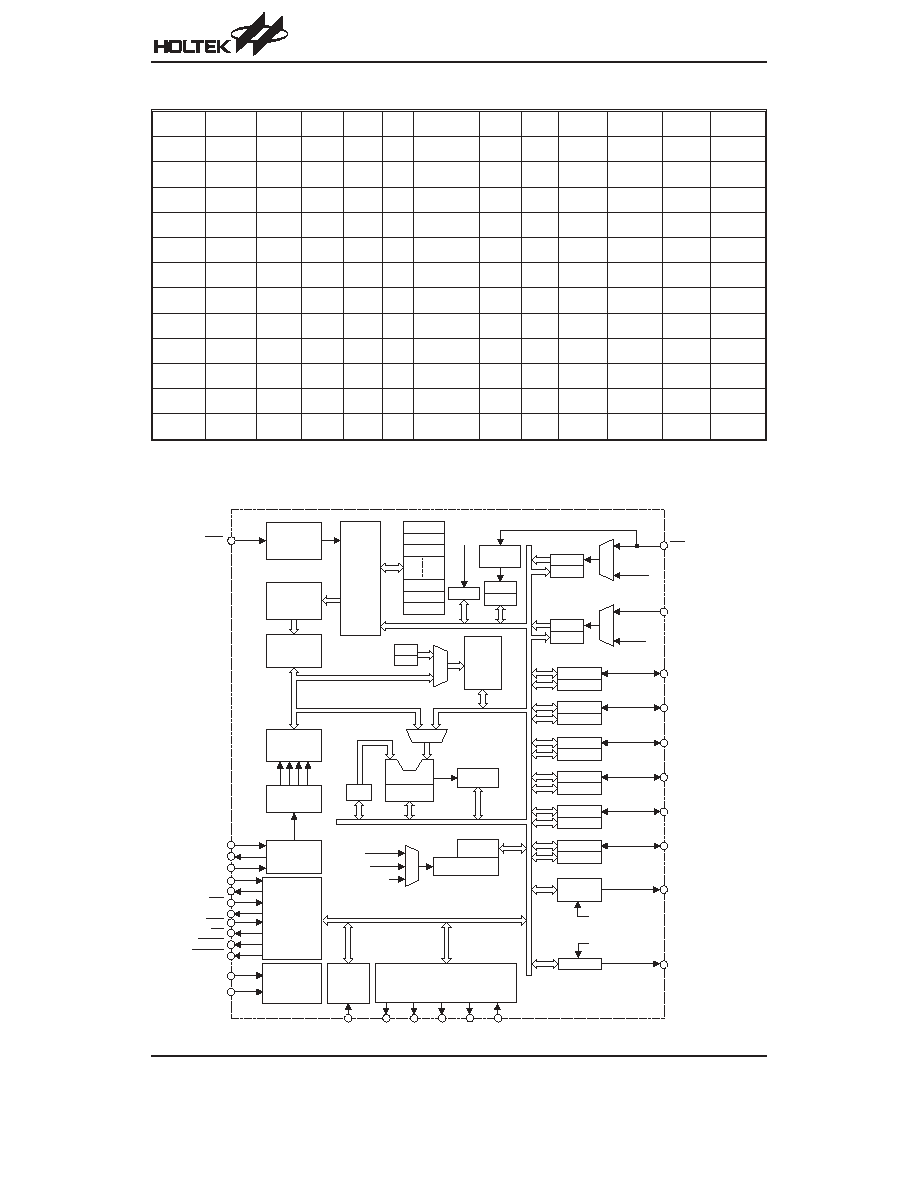
Block Diagram (HT95L400/40P)
HT95LXXX
Rev. 1.20
2
May 26, 2004
P r o g r a m
C o u n t e r
P r o g r a m
R O M
I n s t r u c t i o n
R e g i s t e r
I n s t r u c t i o n
D e c o d e r
T i m i n g
G e n e r a t o r
I N T C 1
I n t e r r u p t
C i r c u i t
M
U
X
M U X
D A T A
M e m o r y
A L U
S h i f t e r
S T A T U S
A C C
L C D D r i v e r
M P 1
M P 0
P o w e r D o w n
D e t e c t o r &
R e s e t C i r c u i t
I N T C 0
R T C
3 2 7 6 8 H z
O S C C i r c u i t
M
U
X
W D T S
W D T P r e s c a l e r
3 2 7 6 8 H z
S y s t e m C l o c k / 4
W D T O S C
T M R 1 C
T M R 1
M
U
X
3 2 7 6 8 H z
T M R 0 C
T M R 0
M
U
X
S y s t e m c l o c k / 4
P F D
I N T / T M R 1
T M R 0
M U S I C
R E S
X 1
X 2
X C
C O M 0 ~ C O M 1 5 S E G 0 ~ S E G 4 7 V L C D
3 2 7 6 8 H z
o r 3 . 5 8 M H z / 4
P o w e r
S u p p l y
V D D
V S S
L o w
B a t t e r y
D e t e c t o r
L B I N
D i a l e r I / O
H F I
H F O
H D I
H D O
H K S
P O
D N P O
X M U T E
D T M F
G e n e r a t o r
D T M F
3 . 5 8 M H z
S T A C K 1 1
S T A C K 1 0
S T A C K 9
S T A C K 0
S T A C K 1
S T A C K 2
P A
P A C
P A 0 ~ P A 7
P B
P B C
P B 0 ~ P B 7
P D
P D C
P D 0 ~ P D 7
P E
P E C
P E 0 ~ P E 3
P F
P F C
P F 0 ~ P F 7
P G
P G C
P G 0 ~ P G 3

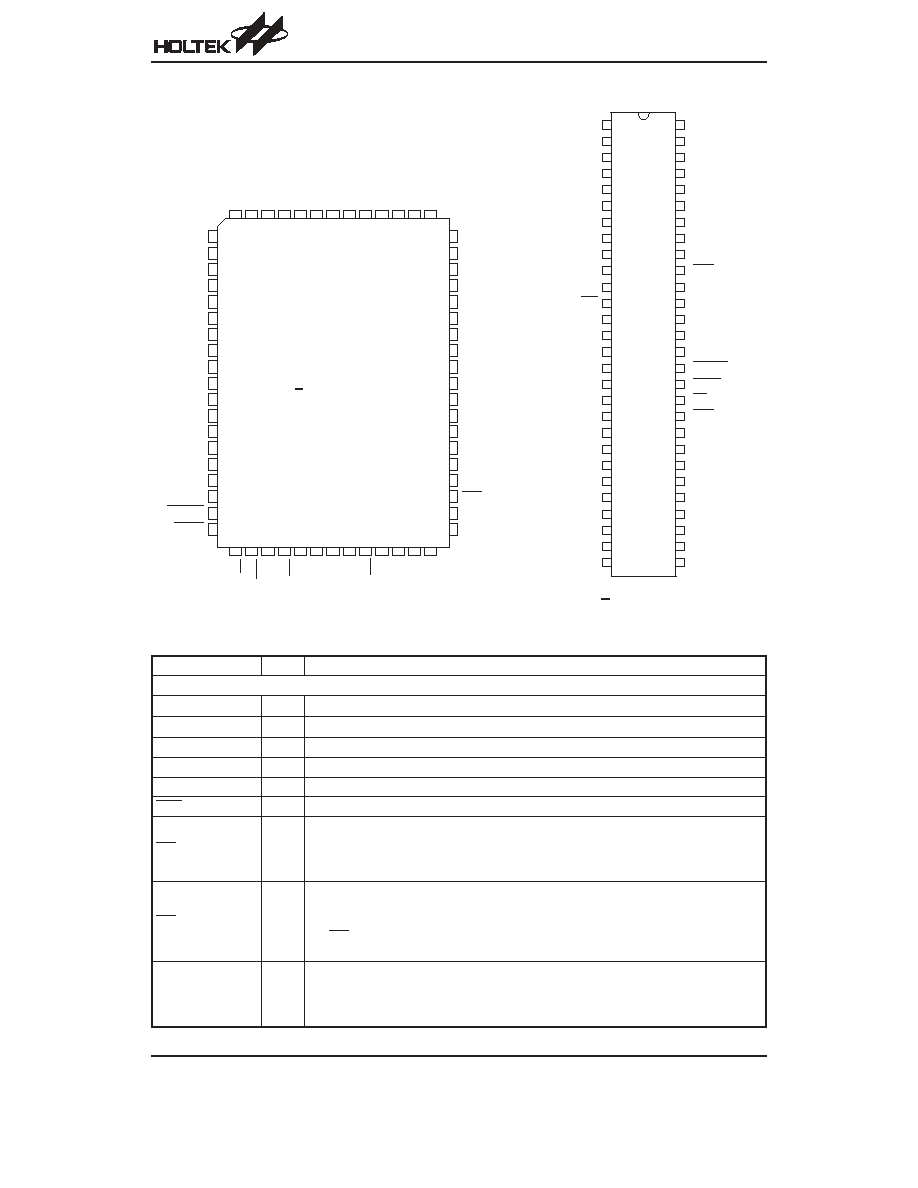
Pin Assignment
HT95L400/40P
HT95LXXX
Rev. 1.20
3
May 26, 2004
1 2 6
1 2 7
H T 9 5 L 4 0 0 / 4 0 P
1 2 8 Q F P - A
N
C
S
E
G
3
3
S
E
G
3
4
S
E
G
3
5
S
E
G
3
6
/
P
D
0
S
E
G
3
7
/
P
D
1
S
E
G
3
8
/
P
D
2
S
E
G
3
9
/
P
D
3
S
E
G
4
0
/
P
D
4
S
E
G
4
1
/
P
D
5
S
E
G
4
2
/
P
D
6
S
E
G
4
3
/
P
D
7
S
E
G
4
4
/
P
E
0
S
E
G
4
5
/
P
E
1
S
E
G
4
6
/
P
E
2
S
E
G
4
7
/
P
E
3
V
L
C
D
M
U
S
I
C
R
E
S
T
M
R
0
D
T
M
F
L
B
I
N
X
C
X
1
X
2
N
C
4 1 4 2 4 3 4 4 4 5 4 6 4 7 4 8 4 9 5 0
4 0
5 1 5 2 5 3
1
2
3
4
5
6
7
8
9
1 0
1 1
1 2
1 3
1 4
1 5
1 6
1 7
1 8
1 9
2 0
2 1
2 2
2 3
2 4
2 5
2 6
2 7
2 8
2 9
3 0
3 1
3 2
3 3
3 4
3 5
3 6
3 7
3 8
1 2 8
P F 6
P F 5
P F 4
P F 3
P F 2
P F 1
P F 0
P A 7
P A 6
P A 5
P A 4
P A 3
P A 2
P A 1
P A 0
P B 7
P B 6
P B 5
P B 4
P B 3
P B 2
P B 1
P B 0
X M U T E
D N P O
P O
H K S
H D O
H D I
H F O
H F I
V S S
V D D
I N T / T M R 1
N C
N C
N C
N C
3 9
5 4 5 5 5 6 5 7 5 8 5 9 6 0 6 1 6 2 6 3 6 4
N C
N C
N C
N C
S E G 3
S E G 4
S E G 5
S E G 6
S E G 7
S E G 8
S E G 9
S E G 1 0
S E G 1 1
S E G 1 2
S E G 1 3
S E G 1 4
S E G 1 5
S E G 1 6
S E G 1 7
S E G 1 8
S E G 1 9
S E G 2 0
S E G 2 1
S E G 2 2
S E G 2 3
S E G 2 4
S E G 2 5
S E G 2 6
S E G 2 7
S E G 2 8
S E G 2 9
S E G 3 0
S E G 3 1
S E G 3 2
N C
N C
N C
N C
S
E
G
2
S
E
G
1
S
E
G
0
C
O
M
1
5
C
O
M
1
4
C
O
M
1
3
C
O
M
1
2
C
O
M
1
1
C
O
M
1
0
C
O
M
9
C
O
M
8
C
O
M
7
C
O
M
6
C
O
M
5
C
O
M
4
C
O
M
3
C
O
M
2
C
O
M
1
C
O
M
0
N
C
N
C
P
G
3
P
G
2
P
G
1
P
G
0
P
F
7
1 2 5
1 2 2
1 2 3
1 2 4
1 2 1 1 2 0 1 1 9 1 1 8 1 1 7 1 1 6 1 1 5 1 1 4 1 1 3 1 1 2 1 1 1 1 1 0 1 0 9 1 0 8 1 0 7 1 0 6 1 0 5 1 0 4 1 0 3
1 0 2
1 0 1
1 0 0
9 9
9 8
9 7
9 6
9 5
9 4
9 3
9 2
9 1
9 0
8 9
8 8
8 7
8 6
8 5
8 4
8 3
8 2
8 1
8 0
7 9
7 8
7 7
7 6
7 5
7 4
7 3
7 2
7 1
7 0
6 9
6 8
6 7
6 6
6 5

HT95L300/30P
HT95L200/20P
HT95LXXX
Rev. 1.20
4
May 26, 2004
H T 9 5 L 2 0 0 / 2 0 P
1 0 0 Q F P - A
1
2
3
4
5
6
7
8
9
1 0
1 1
1 2
1 3
1 4
1 5
1 6
1 7
1 8
1 9
2 0
2 1
2 2
2 3
2 4
2 5
2 6
2 7
2 8
2 9
3 0
3 1 3 2 3 3 3 4 3 5 3 6 3 7 3 8 3 9 4 0 4 1 4 2 4 3 4 4 4 5 4 6 4 7 4 8 4 9 5 0
8 1
8 2
8 3
8 4
8 5
8 6
8 7
8 8
8 9
9 0
9 1
9 2
9 3
9 4
9 5
9 6
9 7
9 8
9 9
1 0 0
8 0
7 9
7 8
7 7
7 6
7 5
7 4
7 3
7 2
7 1
7 0
6 9
6 8
6 7
6 6
6 5
6 4
6 3
6 2
6 1
6 0
5 9
5 8
5 7
5 6
5 5
5 4
5 3
5 2
5 1
N C
N C
N C
N C
N C
N C
N C
P B 5
P B 4
P B 3
P B 2
P B 1
P B 0
X M U T E
D N P O
P O
H K S
H D O
H D I
H F O
H F I
N C
N C
N C
N C
V S S
V D D
I N T / T M R 1
X 2
X 1
N C
N C
N C
N C
C O M 1 0
C O M 1 1
C O M 1 2
C O M 1 3
C O M 1 4
C O M 1 5
S E G 0
S E G 1
S E G 2
S E G 3
S E G 4
S E G 5
S E G 6
S E G 7
S E G 8
S E G 9
S E G 1 0
S E G 1 1
S E G 1 2
S E G 1 3
S E G 1 4
S E G 1 5
N C
N C
N C
N C
C
O
M
9
C
O
M
8
C
O
M
7
/
P
D
7
C
O
M
6
/
P
D
6
C
O
M
5
/
P
D
5
C
O
M
4
/
P
D
4
C
O
M
3
/
P
D
3
C
O
M
2
/
P
D
2
C
O
M
1
/
P
D
1
C
O
M
0
/
P
D
0
P
A
7
P
A
6
P
A
5
P
A
4
P
A
3
P
A
2
P
A
1
P
A
0
P
B
7
P
B
6
S
E
G
1
6
S
E
G
1
7
S
E
G
1
8
S
E
G
1
9
S
E
G
2
0
S
E
G
2
1
S
E
G
2
2
S
E
G
2
3
P
E
0
P
E
1
P
E
2
P
E
3
N
C
V
L
C
D
M
U
S
I
C
R
E
S
T
M
R
0
D
T
M
F
L
B
I
N
X
C
H T 9 5 L 3 0 0 / 3 0 P
1 0 0 Q F P - A
1
2
3
4
5
6
7
8
9
1 0
1 1
1 2
1 3
1 4
1 5
1 6
1 7
1 8
1 9
2 0
2 1
2 2
2 3
2 4
2 5
2 6
2 7
2 8
2 9
3 0
3 1 3 2 3 3 3 4 3 5 3 6 3 7 3 8 3 9 4 0 4 1 4 2 4 3 4 4 4 5 4 6 4 7 4 8 4 9 5 0
8 1
8 2
8 3
8 4
8 5
8 6
8 7
8 8
8 9
9 0
9 1
9 2
9 3
9 4
9 5
9 6
9 7
9 8
9 9
1 0 0
8 0
7 9
7 8
7 7
7 6
7 5
7 4
7 3
7 2
7 1
7 0
6 9
6 8
6 7
6 6
6 5
6 4
6 3
6 2
6 1
6 0
5 9
5 8
5 7
5 6
5 5
5 4
5 3
5 2
5 1
C O M 0
P A 7
P A 6
P A 5
P A 4
P A 3
P A 2
P A 1
P A 0
P B 7
P B 6
P B 5
P B 4
P B 3
P B 2
P B 1
P B 0
X M U T E
D N P O
P O
H K S
H D O
H D I
H F O
H F I
V S S
V D D
I N T / T M R 1
X 2
X 1
S E G 5
S E G 6
S E G 7
S E G 8
S E G 9
S E G 1 0
S E G 1 1
S E G 1 2
S E G 1 3
S E G 1 4
S E G 1 5
S E G 1 6
S E G 1 7
S E G 1 8
S G E 1 9
S E G 2 0
S E G 2 1
S E G 2 2
S E G 2 3
S E G 2 4
S E G 2 5
S E G 2 6
S E G 2 7
S E G 2 8
S E G 2 9
S E G 3 0
S E G 3 1
S E G 3 2
S E G 3 3
S E G 3 4
S
E
G
4
S
E
G
3
S
E
G
2
S
E
G
1
S
E
G
0
C
O
M
1
5
C
O
M
1
4
C
O
M
1
3
C
O
M
1
2
C
O
M
1
1
C
O
M
1
0
C
O
M
9
C
O
M
8
C
O
M
7
C
O
M
6
C
O
M
5
C
O
M
4
C
O
M
3
C
O
M
2
C
O
M
1
S
E
G
3
5
S
E
G
3
6
/
P
D
0
S
E
G
3
7
/
P
D
1
S
E
G
3
8
/
P
D
2
S
E
G
3
9
/
P
D
3
S
E
G
4
0
/
P
D
4
S
E
G
4
1
/
P
D
5
S
E
G
4
2
/
P
D
6
S
E
G
4
3
/
P
D
7
S
E
G
4
4
/
P
E
0
S
E
G
4
5
/
P
E
1
S
E
G
4
6
/
P
E
2
S
E
G
4
7
/
P
E
3
V
L
C
D
M
U
S
I
C
R
E
S
T
M
R
0
D
T
M
F
L
B
I
N
X
C
HT95L100/10P, HT95L000/00P
Pin Description
Pin Name
I/O
Description
CPU
VDD
ĺ
Positive power supply
VSS
ĺ
Negative power supply, ground
X1
I
A 32768Hz crystal (or resonator) should be connected to this pin and X2.
X2
O
A 32768Hz crystal (or resonator) should be connected to this pin and X1.
XC
I
External low pass filter used for frequency up conversion circuit.
RES
I
Schmitt trigger reset input, active low.
INT
I
Supported for HT95L000/00P
Schmitt trigger input for external interrupt
No internal pull-high resistor.
Edge trigger activated on a falling edge.
INT/TMR1
I
Supported for HT95L400/40P, HT95L300/30P, HT95L200/20P, HT95L100/10P
Schmitt trigger input for external interrupt or Timer/Event Counter 1.
No internal pull-high resistor.
For INT: Edge trigger activated on a falling edge.
For TMR1: Activated on falling or rising transition edge, selected by software.
TMR0
I
Supported for HT95L400/40P, HT95L300/30P, HT95L200/20P, HT95L100/10P
Schmitt trigger input for Timer/Event Counter 0.
No internal pull-high resistor.
Activated on falling or rising transition edge, selected by software.
HT95LXXX
Rev. 1.20
5
May 26, 2004
S E G 6
S E G 7
S E G 8
S E G 9
S E G 1 0
S E G 1 1
S E G 1 2
S E G 1 3
S E G 1 4
S E G 1 5
S E G 1 6 / P E 0
S E G 1 7 / P E 1
S E G 1 8 / P E 2
S E G 1 9 / P E 3
V L C D
M U S I C
R E S
T M R 0
D T M F
2 0 2 1 2 2 2 3 2 4 2 5 2 6 2 7 2 8 2 9 3 0 3 1 3 2
1
2
3
4
5
6
7
8
9
1 0
1 1
1 2
1 3
1 4
1 5
1 6
1 7
1 8
1 9
5 1
5 0
4 9
4 8
4 7
4 6
4 5
4 4
4 3
4 2
4 1
4 0
3 9
3 8
3 7
3 6
3 5
3 4
3 3
6 1 6 0 5 9 5 8 5 7 5 6 5 5 5 4 5 3 5 2
6 4 6 3 6 2
C O M 0
P A 7
P A 6
P A 5
P A 4
P A 3
P A 2
P A 1
P A 0
P B 7
P B 6
P B 5
P B 4
P B 3
P B 2
P B 1
P B 0
X M U T E
D N P O
H T 9 5 L 1 0 0 / 1 0 P
6 4 Q F P - A
L
B
I
N
X
C
X
2
X
1
I
N
T
/
T
M
R
1
V
D
D
V
S
S
H
F
I
H
F
O
H
D
I
H
D
O
H
K
S
P
O
S
E
G
5
S
E
G
4
S
E
G
3
S
E
G
2
S
E
G
1
S
E
G
0
C
O
M
7
C
O
M
6
C
O
M
5
C
O
M
4
C
O
M
3
C
O
M
2
C
O
M
1
P A 3
P A 2
P A 1
P A 0
P B 5
P B 4
V S S
P B 3
P B 2
P B 1
P B 0
I N T
C O M 0
C O M 1
C O M 2
C O M 3
C O M 4
C O M 5
C O M 6
C O M 7
S E G 0
S E G 1
S E G 2
S E G 3
S E G 4
S E G 5
S E G 6
S E G 7
P A 4
P A 5
P A 6
P A 7
X 1
X 2
X C
N C
V D D
R E S
D T M F
N C
N C
H F I
H F O
X M U T E
D N P O
P O
H K S
N C
S E G 1 5 / P E 3
S E G 1 4 / P E 2
S E G 1 3 / P E 1
S E G 1 2 / P E 0
S E G 1 1
S E G 1 0
S E G 9
S E G 8
5 6
5 5
5 4
5 3
5 2
5 1
5 0
4 9
4 8
4 7
4 6
4 5
4 4
4 3
4 2
4 1
4 0
3 9
3 8
3 7
3 6
3 5
3 4
3 3
3 2
3 1
3 0
2 9
1
2
3
4
5
6
7
8
9
1 0
1 1
1 2
1 3
1 4
1 5
1 6
1 7
1 8
1 9
2 0
2 1
2 2
2 3
2 4
2 5
2 6
2 7
2 8
H T 9 5 L 0 0 0 / 0 0 P
5 6 S S O P - A

Pin Name
I/O
Description
LCD Driver
SEG47~SEG0
O
or
I/O
LCD panel segment outputs.
Some segment outputs can be optioned to Bidirectional input/output ports by software.
(See the
≤LCD Driver≤ function)
COM15~COM0
O
or
I/O
LCD panel common outputs.
Some common outputs can be optioned to Bidirectional input/output ports by software.
(See the
≤LCD Driver≤ function)
VLCD
I
LCD driver power source.
Normal I/O
PA7~PA0
I/O
Bidirectional input/output ports.
Schmitt trigger input and CMOS output.
See mask option table for pull-high and wake-up function
PB7~PB0
I/O
Bidirectional input/output ports.
Schmitt trigger input and CMOS output.
See mask option table for pull-high function
PD7~PD0
I/O
Bidirectional input/output ports.
Schmitt trigger input and CMOS output.
See mask option table for pull-high function
Port D could be optioned to LCD signal output, see the
≤Input/Output Ports≤ function
PE3~PE0
I/O
Bidirectional input/output ports.
Schmitt trigger input and CMOS output.
See mask option table for pull-high function
Port E could be optioned to LCD signal output, see the
≤Input/Output Ports≤ function
PF7~PF0
I/O
Bidirectional input/output ports.
Schmitt trigger input and CMOS output.
See mask option table for pull-high function
PG3~PG0
I/O
Bidirectional input/output ports.
Schmitt trigger input and CMOS output.
See mask option table for pull-high function
Dialer I/O (See the
≤Dialer I/O Function≤)
HFI
I
Schmitt trigger input structure. An external RC network is recommended for input
debouncing.
This pin is pulled low with internal resistance of 200k
W typ.
HFO
O
CMOS output structure.
HDI
I
Schmitt trigger input structure. An external RC network is recommended for input
debouncing.
This pin is pulled high with internal resistance of 200k
W typ.
HDO
O
CMOS output structure.
HKS
I
This pin detects the status of the hook-switch and its combination with HFI/HDI can con-
trol the PO pin output to make or break the line.
PO
O
CMOS output structure controlled by HKS and HFI/HDI pins and which determines
whether the dialer connects or disconnects the telephone line.
DNPO
O
NMOS output structure.
XMUTE
O
NMOS output structure. Usually, XMUTE is used to mute the speech circuit when trans-
mitting the dialer signal.
Peripherals
DTMF
O
This pin outputs dual tone signals to dial out the phone number. The load resistor should
not be less than 5k
W.
MUSIC
O
This pin outputs the single tone that is generated by the PFD generator.
LBIN
I
This pin detects battery low through external R1/R2 to determine threshold voltage.
HT95LXXX
Rev. 1.20
6
May 26, 2004

Absolute Maximum Ratings
Supply Voltage ..........................V
SS
-0.3V to V
SS
+5.5V
Storage Temperature ...........................
-50įC to 125įC
Input Voltage .............................. V
SS
-0.3 to V
DD
+0.3V
Operating Temperature ..........................
-20įC to 70įC
Note: These are stress ratings only. Stresses exceeding the range specified under
≤Absolute Maximum Ratings≤ may
cause substantial damage to the device. Functional operation of this device at other conditions beyond those
listed in the specification is not implied and prolonged exposure to extreme conditions may affect device reliabil-
ity.
Electrical Characteristics
Ta=25
įC
Symbol
Parameter
Test Conditions
Min.
Typ.
Max.
Unit
V
DD
Conditions
CPU
I
IDL
Idle Mode Current
5V
32768Hz off, 3.58MHz off,
CPU off, LCD off, WDT off,
no load
ĺ
ĺ
2
mA
I
SLP
Sleep Mode Current
5V
32768Hz on, 3.58MHz off,
CPU off, LCD off, WDT off,
no load
ĺ
ĺ
30
mA
I
GRN
Green Mode Current
5V
32768Hz on, 3.58MHz off,
CPU on, LCD off, WDT off,
no load
ĺ
ĺ
50
mA
I
NOR
Normal Mode Current
5V
32768Hz on, 3.58MHz on,
CPU on, LCD on, WDT on,
DTMF generator off, no load
ĺ
ĺ
3
mA
V
IL
I/O Port Input Low Voltage
5V
ĺ
0
ĺ
1
V
V
IH
I/O Port Input High Voltage
5V
ĺ
4
ĺ
5
V
I
OL
I/O Port Sink Current
5V
ĺ
4
6
ĺ
mA
I
OH
I/O Port Source Current
5V
ĺ
-2
-3
ĺ
mA
R
PH
Pull-high Resistor
5V
ĺ
10
30
ĺ
k
W
V
LBIN
Low Battery Detection
Reference voltage
5V
ĺ
1.10
1.15
1.20
V
LCD Driver
V
LCD
LCD Panel Power Supply
ĺ
ĺ
ĺ
3
5
V
I
LCD
LCD Operation Current
ĺ V
LCD
=5V, 32768Hz, no load
ĺ
ĺ
100
mA
Dialer I/O
I
XMO
XMUTE Leakage Current
2.5V XMUTE pin=2.5V
ĺ
ĺ
1
mA
I
OLXM
XMUTE Sink Current
2.5V XMUTE pin=0.5V
1
ĺ
ĺ
mA
I
HKS
HKS Input Current
2.5V HKS pin=2.5V
ĺ
ĺ
0.1
mA
R
HFI
HFI Pull-low Resistance
2.5V V
HFI
=2.5V
ĺ
200
ĺ
k
W
R
HDI
HDI Pull-high Resistance
2.5V V
HDI
=0V
ĺ
200
ĺ
k
W
I
OH2
HFO Source Current
2.5V V
OH
=2V
-1
ĺ
ĺ
mA
I
OL2
HFO Sink Current
2.5V V
OL
=0.5V
1
ĺ
ĺ
mA
I
OH3
HDO Source Current
2.5V V
OH
=2V
-1
ĺ
ĺ
mA
I
OL3
HDO Sink Current
2.5V V
OL
=0.5V
1
ĺ
ĺ
mA
I
OH4
PO Source Current
2.5V V
OH
=2V
-1
ĺ
ĺ
mA
I
OL4
PO Sink Current
2.5V V
OL
=0.5V
1
ĺ
ĺ
mA
I
OL5
DNPO Sink Current
2.5V V
OL
=0.5V
1
ĺ
ĺ
mA
HT95LXXX
Rev. 1.20
7
May 26, 2004

Symbol
Parameter
Test Conditions
Min.
Typ.
Max.
Unit
V
DD
Conditions
DTMF Generator
V
TDC
DTMF Output DC Level
ĺ
ĺ
0.45V
DD
ĺ
0.7V
DD
V
V
TOL
DTMF Sink Current
ĺ V
DTMF
=0.5V
0.1
ĺ
ĺ
mA
V
TAC
DTMF Output AC Level
ĺ Row group, R
L
=5k
W
120
155
180
mVrms
R
L
DTMF Output Load
ĺ THD£-23dB
5
ĺ
ĺ
k
W
A
CR
Column Pre-emphasis
ĺ Row group=0dB
1
2
3
dB
THD
Tone Signal Distortion
ĺ R
L
=5k
W
ĺ
-30
-23
dB
HT95LXXX
Rev. 1.20
8
May 26, 2004
Functional Description
Execution Flow
The system clock for the telephone controller is derived
from a 32768Hz crystal oscillator. A built-in frequency up
conversion circuit provides dual system clock, namely;
32768Hz and 3.58MHz. The system clock is internally
divided into four non-overlapping clocks. One instruc-
tion cycle consists of four system clock cycles. Instruc-
tion fetching and execution are pipelined in such a way
that a fetch takes an instruction cycle while decoding
and execution takes the next instruction cycle. The
pipelining scheme causes each instruction to be effec-
tively executed in a instruction cycle. If an instruction
changes the program counter, two instruction cycles are
required to complete the instruction.
Program Counter
- PC
The program counter (PC) controls the sequence in
which the instructions stored in the program ROM are
executed and its contents specify a full range of pro-
gram memory. After accessing a program memory word
to fetch an instruction code, the contents of the program
counter are incremented by 1. The program counter
then points to the memory word containing the next in-
struction code.
When executing a jump instruction, conditional skip ex-
ecution, loading PCL register, subroutine call, initial re-
set, internal interrupt, external interrupt or return from
subroutine, the program counter manipulates the pro-
gram transfer by loading the address corresponding to
each instruction. The conditional skip is activated by
instructions. Once the condition is met, the next instruc-
tion, fetched during the current instruction execution, is
discarded and a dummy cycle replaces it to get the
proper instruction. Otherwise proceed to the next in-
struction.
The program counter lower order byte register
(PCL:06H) is a readable and write-able register. Moving
data into the PCL performs a short jump. The destina-
tion will be within 256 locations. When a control transfer
takes place, an additional dummy cycle is required.
Program Memory
- ROM
The program memory is used to store the program in-
structions which are to be executed. It also contains
data, table, and interrupt entries, and is organized into
8K
ī16 bitsī2 banks (HT95L400/40P), 8Kī16 bits
(HT95L300/30P, HT95L200/20P) or 4K
ī16 bits
(HT95L100/10P, HT95L000/00P), addressed by the
program counter and table pointer.
For the HT95L400/40P, the program memory is divided
into 2 banks, each bank having a ROM Size 8K
ī16 bits.
To move from the present ROM bank to a different ROM
bank, the higher 1 bits of the ROM address are set by
the BP (Bank Pointer), while the remaining 13 bits of the
PC are set in the usual way by executing the appropriate
jump or call instruction. As the 14 address bits are
latched during the execution of a call or jump instruction,
the correct value of the BP must first be setup before a
T 1
T 2
T 3
T 4
T 1
T 2
T 3
T 4
T 1
T 2
T 3
T 4
F e t c h I N S T ( P C )
E x e c u t e I N S T ( P C - 1 )
F e t c h I N S T ( P C + 1 )
E x e c u t e I N S T ( P C )
F e t c h I N S T ( P C + 2 )
E x e c u t e I N S T ( P C + 1 )
P C
P C + 1
P C + 2
S y s t e m C l o c k
P C
Execution Flow

HT95LXXX
Rev. 1.20
9
May 26, 2004
jump or call is executed. When either a software or hard-
ware interrupt is received, note that no matter which
ROM bank the program is in, the program will always
jump to the appropriate interrupt service address in
Bank 0. The original 14 bits address will be stored on the
stack and restored when the relevant RET/RETI instruc-
tion is executed, automatically returning the program to
the original ROM bank. This eliminates the need for pro-
grammers to manage the BP when interrupts occur.
Certain locations in the program memory are reserved
for special usage:
∑
Location 0000H (Bank0)
This area is reserved for the initialization program. Af-
ter chip power-on reset or external reset or WDT
time-out reset, the program always begins execution
at location 0000H.
∑
Location 0004H (Bank0)
This area is reserved for the external interrupt service
program. If the INT/TMR1 input pin is activated, the
external interrupt is enabled and the stack is not full,
the program begins execution at location 0004H.
∑
Location 0008H (Bank0)
This area is reserved for the Timer/Event Counter 0 in-
terrupt service program. If a timer interrupt results
from a Timer/Event Counter 0 overflow, the
Timer/Event Counter 0 interrupt is enabled and the
stack is not full, the program begins execution at loca-
tion 0008H.
Mode
Program Counter
*13
*12
*11
*10
*9
*8
*7
*6
*5
*4
*3
*2
*1
*0
Initial reset
0
0
0
0
0
0
0
0
0
0
0
0
0
0
External interrupt
0
0
0
0
0
0
0
0
0
0
0
1
0
0
Timer/Event Counter 0 overflow
0
0
0
0
0
0
0
0
0
0
1
0
0
0
Timer/Event Counter 1 overflow
0
0
0
0
0
0
0
0
0
0
1
1
0
0
RTC interrupt
0
0
0
0
0
0
0
0
0
1
0
1
0
0
Dialer I/O interrupt
0
0
0
0
0
0
0
0
0
1
1
0
0
0
Skip
Program Counter+2 (within current bank)
Loading PCL
*13
*12
*11
*10
*9
*8
@7
@6
@5
@4
@3
@2
@1
@0
Jump, call branch
BP.5 #12 #11 #10
#9
#8
#7
#6
#5
#4
#3
#2
#1
#0
Return from subroutine
S13 S12 S11 S10
S9
S8
S7
S6
S5
S4
S3
S2
S1
S0
Program ROM Address
Note: *13~*0: Program counter bits
S13~S0: Stack register bits
#12~#0: Instruction code bits
@7~@0: PCL bits
Available bits of program counter for HT95L400/40P: Bit 13~Bit 0
Available bits of program counter for HT95L300/30P: Bit 12~Bit 0
Available bits of program counter for HT95L200/20P: Bit 12~Bit 0
Available bits of program counter for HT95L100/10P: Bit 11~Bit 0
Available bits of program counter for HT95L000/00P: Bit 11~Bit 0
0 0 0 H
0 0 4 H
0 0 8 H
D e v i c e I n i t i a l i z a t i o n P r o g r a m
E x t e r n a l I n t e r r u p t S u b r o u t i n e
T i m e r / E v e n t C o u n t e r 0 I n t e r r u p t S u b r o u t i n e
P r o g r a m
R O M
1 6 b i t s
L o o k - u p T a b l e ( 2 5 6 W o r d s )
1 0 0 H
L o o k - u p T a b l e ( 2 5 6 W o r d s )
( L a s t P a g e s )
N o t e : T h e L a s t p a g e f o r H T 9 5 L 4 0 0 / 4 0 P i s 3 F 0 0 H ~ 3 F F F H
T h e L a s t p a g e f o r H T 9 5 L 3 0 0 / 3 0 P i s 1 F 0 0 H ~ 1 F F F H
T h e L a s t p a g e f o r H T 9 5 L 2 0 0 / 2 0 P i s 1 F 0 0 H ~ 1 F F F H
T h e L a s t p a g e f o r H T 9 5 L 1 0 0 / 1 0 P i s 0 F 0 0 H ~ 0 F F F H
T h e L a s t p a g e f o r H T 9 5 L 0 0 0 / 0 0 P i s 0 F 0 0 H ~ 0 F F F H
1 F F H
T i m e r / E v e n t C o u n t e r 1 I n t e r r u p t S u b r o u t i n e
0 0 C H
0 1 0 H
R T C I n t e r r u p t S u b r o u t i n e
0 1 4 H
D i a l e r I / O I n t e r r u p t S u b r o u t i n e
0 1 8 H
R e s e r v e d
Program Memory

HT95LXXX
Rev. 1.20
10
May 26, 2004
∑
Location 000CH (Bank0)
This location is reserved for the Timer/Event Counter
1 interrupt service program. If a timer interrupt results
from a Timer/Event Counter 1 overflow, the
Timer/Event Counter 1 interrupt is enabled and the
stack is not full, the program begins execution at loca-
tion 000CH.
∑
Location 0014H (Bank0)
This location is reserved for real time clock (RTC) in-
terrupt service program. When RTC generator is en-
abled and time-out occurs, the RTC interrupt is
enabled and the stack is not full, the program begins
execution at location 0014H.
∑
Location 0018H (Bank0)
This location is reserved for the HKS pin edge transi-
tion or HDI pin falling edge transition or HFI pin rising
edge transition. If this condition occurs, the dialer I/O
interrupt is enabled and the stack is not full, the pro-
gram begins execution at location 18H.
Table Location
Any location in the ROM space can be used as look-up
tables. The instructions
≤TABRDC [m]≤ (the current
page, one page=256 words) and
≤TABRDL [m]≤ (the last
page) transfer the contents of the lower-order byte to the
specified data memory, and the higher-order byte to
TBLH (08H). For the HT95L400/40P, the instruction
≤TABRDC [m]≤ is used for any page of any bank. Only
the destination of the lower-order byte in the table is
well-defined, and the higher-order byte of the table word
is transferred to TBLH. The table pointer (TBLP) or
(TBHP, TBLP for the HT95L400/40P) is a read/write
register (07H) or (1FH, 07H for the HT95L400/40P),
which indicates the table location. Before accessing the
table, the location must be placed in the (TBLP) or
(TBHP, TBLP for the HT95L400/40P). The TBLH is read
only and cannot be restored. If the main routine and the
ISR (Interrupt Service Routine) both employ the table
read instruction, the contents of the TBLH in the main
routine are likely to be changed by the table read in-
struction used in the ISR. Errors will then occur. Hence,
simultaneously using the table read instruction in the
main routine and the ISR should be avoided. However, if
the table read instruction has to be applied in both the
main routine and the ISR, the interrupt should be dis-
abled prior to the table read instruction. It will not be en-
abled until the TBLH has been backed-up. All table
related instructions require two cycles to complete the
operation. These areas may function as normal pro-
gram memory depending on the requirements.
HT95L400/40P
Instruction(s)
Table Location
*13
*12
*11
*10
*9
*8
*7
*6
*5
*4
*3
*2
*1
*0
TABRDC [m]
#5
#4
#3
#2
#1
#0
@7
@6
@5
@4
@3
@2
@1
@0
TABRDL [m]
1
1
1
1
1
1
@7
@6
@5
@4
@3
@2
@1
@0
HT95L300/30P, HT95L200/20P
Instruction(s)
Table Location
*12
*11
*10
*9
*8
*7
*6
*5
*4
*3
*2
*1
*0
TABRDC [m]
P12
P11
P10
P9
P8
@7
@6
@5
@4
@3
@2
@1
@0
TABRDL [m]
1
1
1
1
1
@7
@6
@5
@4
@3
@2
@1
@0
HT95L100/10P, HT95L000/00P
Instruction(s)
Table Location
*11
*10
*9
*8
*7
*6
*5
*4
*3
*2
*1
*0
TABRDC [m]
P11
P10
P9
P8
@7
@6
@5
@4
@3
@2
@1
@0
TABRDL [m]
1
1
1
1
@7
@6
@5
@4
@3
@2
@1
@0
Note: *13~*0: Table location bits
#7~#0: TBHP register bit7~bit0
@7~@0: TBLP register bit7~bit0
P12~P8: Current program counter bits

HT95LXXX
Rev. 1.20
11
May 26, 2004
Special Register, Embedded Control Register, LCD Display Memory and General Purpose RAM
BP
(RAM Bank)
Address
Function
Description
Supported for HT95LXXX
400/P 300/P 200/P 100/P 000/P
Special Function Register
00H
00H
IAR0
Indirect addressing register 0
÷
÷
÷
÷
÷
00H
01H
MP0
Memory pointer register 0
÷
÷
÷
÷
÷
00H
02H
IAR1
Indirect addressing register 1
÷
÷
÷
÷
÷
00H
03H
MP1
Memory pointer register 1
÷
÷
÷
÷
÷
00H
04H
BP
Bank Pointer register
÷
÷
÷
÷
÷
00H
05H
ACC
Accumulator
÷
÷
÷
÷
÷
00H
06H
PCL
Program counter lower-order byte register
÷
÷
÷
÷
÷
00H
07H
TBLP
Table pointer
÷
÷
÷
÷
÷
00H
08H
TBLH
Table higher-order byte register
÷
÷
÷
÷
÷
00H
09H
WDTS
Watchdog Timer option setting register
÷
÷
÷
÷
÷
00H
0AH
STATUS
Status register
÷
÷
÷
÷
÷
00H
0BH
INTC0
Interrupt control register 0
÷
÷
÷
÷
÷
00H
0CH
TMR0H
Timer/Event Counter 0 high-order byte
register
÷
÷
÷
÷
÷
Stack Register
This is a special part of the memory which is used to
save the contents of the program counter only. The
stack is organized into 12 levels (HT95L400/40P), 8 lev-
els (HT95L300/30P, HT95L200/20P, HT95L100/10P) or
4 levels (HT95L000/00P) and is neither part of the data
nor part of the program space, and is neither readable
nor writable. The activated level is indexed by the stack
pointer (SP) and is neither readable nor writable. At a
subroutine call or interrupt acknowledge signal, the con-
tents of the program counter are pushed onto the stack.
At the end of a subroutine or an interrupt routine, sig-
naled by a return instruction (RET or RETI), the program
counter is restored to its previous value from the stack.
After a chip reset, the SP will point to the top of the stack.
If the stack is full and an interrupt takes place, the inter-
rupt request flag will be recorded but the acknowledge
signal will be inhibited even if this interrupt is enabled.
When the stack pointer is decremented (by RET or
RETI), the interrupt will be serviced. This feature pre-
vents stack overflow allowing the programmer to use the
structure more easily. If the stack is full and a
≤CALL≤ is
subsequently executed, stack overflow occurs and the
first entry will be lost (only the most recent 12, 8 or 4, de-
pending on various MCU type, returned addresses are
stored).
Data Memory
The data memory is divided into four functional groups:
special function registers, embedded control register,
LCD display memory and general purpose memory.
Most are read/write, but some are read only.
The special function registers are located from 00H to
1FH. The embedded control registers are located in the
memory areas from 20H to 3FH. The remaining spaces
which are not specified in the following table before the
40H are reserved for future expanded usage and read-
ing these locations will get
≤00H≤. The general purpose
data memory is divided into 15 banks (HT95L400/40P),
11 banks (HT95L300/30P), 6 banks (HT95L200/20P,
HT95L100/10P) or 2 banks (HT95L000/00P). The
banks in the RAM are all addressed from 40H to 0FFH
and they are selected by setting the value of the bank
pointer (BP).
All of the data memory areas can handle arithmetic,
logic, increment, decrement and rotate operations di-
rectly. Except for some dedicated bits, each bit in the
data memory can be set and reset by
≤SET [m].i≤ and
≤CLR [m].i≤. They are also indirectly accessible through
memory pointer registers (MP0 or MP1). The
bank1~bank14 and bank27 are only indirectly accessi-
ble through memory pointer 1 register (MP1).
The LCD display memory is located at bank 1BH. They
can be read and written to by the indirect addressing
mode using memory pointer 1 (MP1). To turn the display
On or Off, a
≤1≤ or ≤0≤ is written to the corresponding bit
of the memory area.

HT95LXXX
Rev. 1.20
12
May 26, 2004
BP
(RAM Bank)
Address
Function
Description
Supported for HT95LXXX
400/P 300/P 200/P 100/P 000/P
00H
0DH
TMR0L
Timer/Event Counter 0 low-order byte
register
÷
÷
÷
÷
÷
00H
0EH
TMR0C
Timer/Event Counter 0 control register
÷
÷
÷
÷
÷
00H
0FH
TMR1H
Timer/Event Counter 1 high-order byte
register
÷
÷
÷
÷
÷
00H
10H
TMR1L
Timer/Event Counter 1 low-order byte
register
÷
÷
÷
÷
÷
00H
11H
TMR1C
Timer/Event Counter 1 control register
÷
÷
÷
÷
÷
00H
12H
PA
Port A data register
÷
÷
÷
÷
÷
00H
13H
PAC
Port A control register
÷
÷
÷
÷
÷
00H
14H
PB
Port B data register
÷
÷
÷
÷
÷
00H
15H
PBC
Port B control register
÷
÷
÷
÷
÷
00H
16H
DIALERIO
Dialer I/O register
÷
÷
÷
÷
÷
00H
18H
PD
Port D data register
÷
÷
÷
ĺ
ĺ
00H
19H
PDC
Port D control register
÷
÷
÷
ĺ
ĺ
00H
1AH
PE
Port E data register
÷
÷
÷
÷
÷
00H
1BH
PEC
Port E control register
÷
÷
÷
÷
÷
00H
1EH
INTC1
Interrupt control register 1
÷
÷
÷
÷
÷
00H
1FH
TBHP
Table high-order byte pointer
÷
ĺ
ĺ
ĺ
ĺ
Embedded Control Register
00H
20H
DTMFC
DTMF generator control register
÷
÷
÷
÷
÷
00H
21H
DTMFD
DTMF generator data register
÷
÷
÷
÷
÷
00H
22H
LINE
Line control register
÷
÷
÷
÷
ĺ
00H
24H
RTCC
Real time clock control register
÷
÷
÷
÷
÷
00H
26H
MODE
Operation mode control register
÷
÷
÷
÷
÷
00H
28H
LCDIO
LCD segment and I/O option register
÷
÷
ĺ
÷
÷
00H
2DH
LCDC
LCD driver control register
÷
÷
÷
÷
÷
00H
2EH
PFDC
PFD control register
÷
÷
÷
÷
ĺ
00H
2FH
PFDD
PFD data register
÷
÷
÷
÷
ĺ
00H
34H
PF
Port F data register
÷
ĺ
ĺ
ĺ
ĺ
00H
35H
PFC
Port F control register
÷
ĺ
ĺ
ĺ
ĺ
00H
36H
PG
Port G data register
÷
ĺ
ĺ
ĺ
ĺ
00H
37H
PGC
Port G control register
÷
ĺ
ĺ
ĺ
ĺ
General Purpose RAM
00H
40H~FFH BANK0 RAM General purpose RAM space
÷
÷
÷
÷
÷
01H
40H~FFH BANK1 RAM General purpose RAM space
÷
÷
÷
÷
÷
02H
40H~FFH BANK2 RAM General purpose RAM space
÷
÷
÷
÷
ĺ
03H
40H~FFH BANK3 RAM General purpose RAM space
÷
÷
÷
÷
ĺ
04H
40H~FFH BANK4 RAM General purpose RAM space
÷
÷
÷
÷
ĺ
05H
40H~FFH BANK5 RAM General purpose RAM space
÷
÷
÷
÷
ĺ
06H
40H~FFH BANK6 RAM General purpose RAM space
÷
÷
ĺ
ĺ
ĺ
07H
40H~FFH BANK7 RAM General purpose RAM space
÷
÷
ĺ
ĺ
ĺ
08H
40H~FFH BANK8 RAM General purpose RAM space
÷
÷
ĺ
ĺ
ĺ

HT95LXXX
Rev. 1.20
13
May 26, 2004
BP
(RAM Bank)
Address
Function
Description
Supported for HT95LXXX
400/P 300/P 200/P 100/P 000/P
09H
40H~FFH BANK9 RAM General purpose RAM space
÷
÷
ĺ
ĺ
ĺ
0AH
40H~FFH BANK10 RAM General purpose RAM space
÷
÷
ĺ
ĺ
ĺ
0BH
40H~FFH BANK11 RAM General purpose RAM space
÷
ĺ
ĺ
ĺ
ĺ
0CH
40H~FFH BANK12 RAM General purpose RAM space
÷
ĺ
ĺ
ĺ
ĺ
0DH
40H~FFH BANK13 RAM General purpose RAM space
÷
ĺ
ĺ
ĺ
ĺ
0EH
40H~FFH BANK14 RAM General purpose RAM space
÷
ĺ
ĺ
ĺ
ĺ
LCD RAM Display Memory
1BH
40H~9FH
LCD RAM
LCD RAM mapping space for COM0~COM15 (see
≤LCD Driver≤ function)
Indirect Addressing Register
Location 00H and 02H are indirect addressing registers
that are not physically implemented. Any read/write op-
eration of [00H] and [02H] will access the memory
pointed to by MP0 and MP1, respectively. Reading loca-
tion [00H] or [02H] indirectly returns the result 00H,
while writing it leads to no operation. MP0 is indirectly
addressable in bank0, but MP1 is available for all banks
by switch BP [04H]. If BP is unequal to 00H, the indirect
addressing mode to read/write operation from 00H~3FH
will return the result as same as the value of bank0.
The memory pointer registers MP0 and MP1 are 8-bits
registers, and the bank pointer register BP is 6-bits reg-
ister for the HT95L400/40P or 5-bits for the other de-
vices in the series.
Accumulator
The accumulator is closely related to ALU operations. It
is also mapped to location 05H of the data memory and
can operate with immediate data. All data movement
between two data memory locations must pass through
the accumulator.
Arithmetic and Logic Unit
- ALU
This circuit performs 8-bit arithmetic and logic opera-
tions and provides the following functions:
∑
Arithmetic operations (ADD, ADC, SUB, SBC, DAA)
∑
Logic operations (AND, OR, XOR, CPL)
∑
Rotation (RL, RR, RLC, RRC)
∑
Increment and Decrement (INC, DEC)
∑
Branch decision (SZ, SNZ, SIZ, SDZ, etc.)
The ALU not only saves the results of a data operation
but also changes the status register.
Status Register
- STATUS
This status register contains the carry flag (C), auxiliary
carry flag (AC), zero flag (Z), overflow flag (OV), power
down flag (PDF), and watchdog time-out flag (TO). It
also records the status information and controls the op-
eration sequence.
Except for the TO and PDF flags, bits in the status regis-
ter can be altered by instructions, similar to the other
registers. Data written into the status register will not
change the TO or PDF flag. Operations related to the
Register
Label
Bits
Function
STATUS
(0AH)
C
0
C is set if the operation results in a carry during an addition operation or if a borrow
does not take place during a subtraction operation; otherwise C is cleared. Also it is
affected by a rotate through carry instruction.
AC
1
AC is set if the operation results in a carry out of the low nibbles in addition or no bor-
row from the high nibble into the low nibble in subtraction; otherwise AC is cleared.
Z
2
Z is set if the result of an arithmetic or logic operation is 0; otherwise Z is cleared.
OV
3
OV is set if the operation results in a carry into the highest-order bit but not a carry
out of the highest-order bit, or vice versa; otherwise OV is cleared.
PDF
4
PDF is cleared when either a system power-up or executing the
≤CLR WDT≤ in-
struction. PDF is set by executing the
≤HALT≤ instruction.
TO
5
TO is cleared by a system power-up or executing the
≤CLR WDT≤ or ≤HALT≤ in-
struction. TO is set by a WDT time-out.
ĺ
6, 7
Unused bit, read as
≤0≤

HT95LXXX
Rev. 1.20
14
May 26, 2004
status register may yield different results from those in-
tended. The TO flag can be affected only by system
power-up, a WDT time-out or executing the
≤CLR WDT≤
or
≤HALT≤ instruction. The PDF flag can be affected
only by executing the
≤HALT≤ or ≤CLR WDT≤ instruction
or during a system power-up.
The Z, OV, AC and C flags generally reflect the status of
the latest operations.
On entering the interrupt sequence or executing the
subroutine call, the status register will not be automati-
cally pushed onto the stack.
If the contents of the status are important and if the sub-
routine can corrupt the status register, precautions must
be taken to save it .
Interrupt
The telephone controller provides an external interrupt,
internal timer/event counter interrupt, an internal real
time clock interrupt and internal dialer I/O interrupt. The
Interrupt Control Registers 0 and Interrupt Control Reg-
ister 1 both contains the interrupt control bits that set the
enable/disable and the interrupt request flags.
Once an interrupt subroutine is serviced, all the other in-
terrupts will be blocked (by hardware clearing the EMI
bit). This scheme may prevent any further interrupt nest-
ing. Other interrupt requests may occur during this inter-
val but only the interrupt request flag is recorded. If a
certain interrupt requires servicing within the service
routine, the EMI bit and the corresponding bit of the
INTC0 (INTC1) may be set to allow interrupt nesting.
If the stack is full, any other interrupt request will not be
acknowledged, even if the related interrupt is enabled,
until the stack pointer is decremented. If immediate ser-
vice is desired, the stack must be prevented from be-
coming full.
All these kinds of interrupts have a wake-up capability.
As an interrupt is serviced, a control transfer occurs by
pushing the program counter onto the stack, followed by
a branch to a subroutine at specified location in the pro-
gram memory. Only the program counter is pushed onto
the stack. If the contents of the register or status register
(STATUS) are altered by the interrupt service program
which corrupts the desired control sequence, the con-
tents should be saved in advance.
External interrupt is triggered by a high to low transition
of the INT/TMR1 pin and the interrupt request flag EIF
will be set. When the external interrupt is enabled, the
stack is not full and the external interrupt is active, a sub-
routine call to location 04H will occur. The interrupt re-
quest flag EIF and EMI bits will be cleared to disable
other interrupts.
The Timer/Event Counter 0 interrupt is generated by a
timeout overflow and the interrupt request flag T0F will
be set. When the Timer/Event Counter 0 interrupt is en-
abled, the stack is not full and the T0F bit is set, a sub-
routine call to location 08H will occur. The interrupt
request flag T0F and EMI bits will be cleared to disable
further interrupts.
The Timer/Event Counter 1 interrupt is generated by a
timeout overflow and the interrupt request flag T1F will
be set. When the Timer/Event Counter 1 interrupt is en-
abled, the stack is not full and the T1F bit is set, a sub-
Register
Bits
Label
R/W
Function
INTC0
(0BH)
0
EMI
RW
Controls the master (global) interrupt (1=enabled; 0=disabled)
1
EEI
RW
Controls the external interrupt (1=enabled; 0=disabled)
2
ET0I
RW
Controls the Timer/Event Counter 0 interrupt (1=enabled; 0=disabled)
3
ET1I
RW
Controls the Timer/Event Counter 1 interrupt (1=enabled; 0=disabled)
4
EIF
RW
External interrupt request flag (1=active; 0=inactive)
5
T0F
RW
Timer/Event Counter 0 request flag (1=active; 0=inactive)
6
T1F
RW
Timer/Event Counter 1 request flag (1=active; 0=inactive)
7
ĺ
RO
Unused bit, read as
≤0≤
INTC1
(1EH)
0
ĺ
RW
Reserved, inhibit using
1
ERTCI
RW
Control the real time clock interrupt (1=enable; 0=disable)
2
EDRI
RW
Control the dialer I/O interrupt (1=enable; 0=disable)
3
ĺ
RO
Unused bit, read as
≤0≤
4
ĺ
RW
Reserved, inhibit using
5
RTCF
RW
Internal real time clock interrupt request flag (1=active; 0=inactive)
6
DRF
RW
Internal dialer I/O interrupt request flag (1=active: 0=inactive)
7
ĺ
RO
Unused bit, read as
≤0≤

HT95LXXX
Rev. 1.20
15
May 26, 2004
routine call to location 0CH will occur. The interrupt
request flag T1F and EMI bits will be cleared to disable
further interrupts.
The real time clock interrupt is generated by a 1Hz RTC
generator. When the RTC time-out occurs, the interrupt
request flag RTCF will be set. When the RTC interrupt is
enabled, the stack is not full and the RTCF is set, a sub-
routine call to location 14H will occur. The interrupt re-
quest flag RTCF and EMI bits will be cleared to disable
other interrupts.
The dialer I/O interrupt is triggered by any edge transi-
tion onto HKS pin or a falling edge transition onto HDI
pin or a rising edge transition onto HFI pin, the interrupt
request flag DRF will be set. When the dialer I/O inter-
rupt is enabled, the stack is not full and the DRF is set, a
subroutine call to location 18H will occur. The interrupt
request flag DRF and EMI bits will be cleared to disable
other interrupts.
Note: 1. If the dialer status is on-hook and hold-line,
the falling edge transition onto HDI pin will not
generate the dialer I/O interrupt.
2. The HDI input is supported for HT95L400/40P,
HT95L300/30P, HT95L200/20P,
HT95L100/10P.
3. The dialer I/O interrupt will be disabled when
the operation mode is in Idle mode.
During the execution of an interrupt subroutine, other in-
terrupt acknowledge signals are held until the RETI in-
struction is executed or the EMI bit and the related
interrupt control bit are set to 1 (if the stack is not full). To
return from the interrupt subroutine,
≤RET≤ or ≤RETI≤
may be invoked. RETI will set the EMI bit to enable an
interrupt service, but RET will not.
Interrupts, occurring in the interval between the rising
edges of two consecutive T2 pulses, will be serviced on
the latter of the two T2 pulses, if the corresponding inter-
rupts are enabled. In the case of simultaneous requests
the following table shows the priority that is applied.
These can be masked by resetting the EMI bit.
Interrupt Source
Priority
Vector
External interrupt
1
04H
Timer/Event Counter 0 interrupt
2
08H
Timer/Event Counter 1 interrupt
3
0CH
Real time clock interrupt
4
14H
Dialer I/O interrupt
5
18H
Priority of the Interrupt
EMI, EEI, ET0I, ET1I, ERTCI and EDRI are used to con-
trol the enabling/disabling of interrupts. These bits pre-
vent the requested interrupt from being serviced. Once
the interrupt request flags (EIF, T0F, T1F, RTCF, DRF)
are set by hardware or software, they will remain in the
INTC0 or INTC1 registers until the interrupts are ser-
viced or cleared by a software instruction.
It is recommended that a program should not use the
≤CALL subroutine≤ within the interrupt subroutine. Inter-
rupts often occur in an unpredictable manner or need to
be serviced immediately in some applications. If only
one stack is left and enabling the interrupt is not well
controlled, the original control sequence will be dam-
aged once the
≤CALL≤ operates in the interrupt subrou-
tine.
Oscillator Configuration
There are two oscillator circuits in the controller, the ex-
ternal 32768Hz crystal oscillator and internal WDT
OSC.
The 32768Hz crystal oscillator and frequency-up con-
version circuit (32768Hz to 3.58MHz) are designed for
dual system clock source. It is necessary for frequency
conversion circuit to add external RC components to
make up the low pass filter that stabilize the output fre-
quency 3.58MHz (see the oscillator circuit).
The WDT OSC is a free running on-chip RC oscillator,
and no external components are required. Even if the
system enters the Idle mode (the system clock is
stopped), the WDT OSC still works within a period of
78
ms normally. When the WDT is disabled or the WDT
source is not this RC oscillator, the WDT OSC will be
disabled.
Watchdog Timer
- WDT
The WDT clock source is implemented by a WDT OSC
or external 32768Hz or an instruction clock (system
clock divided by 4), determined by the mask option. This
timer is designed to prevent a software malfunction or
sequence from jumping to an unknown location with un-
predictable results. The Watchdog Timer can be dis-
abled by mask option. If the Watchdog Timer is disabled,
all the executions related to the WDT result in no opera-
tion.
If the device operates in a noisy environment, using the
on-chip WDT OSC or 32768Hz crystal oscillator is
strongly recommended.
When the WDT clock source is selected, it will be first di-
vided by 512 (9-stage) to get the nominal time-out pe-
riod. By invoking the WDT prescaler, longer time-out
periods can be realized. Writing data to WS2, WS1,
WS0 can give different time-out periods.
X 1
X 2
X C
1 5 k W
3 n F
5 0 n F
System Oscillator Circuit

HT95LXXX
Rev. 1.20
16
May 26, 2004
The WDT OSC period is 78
ms. This time-out period may
vary with temperature, VDD and process variations. The
WDT OSC always works for any operation mode.
If the instruction clock is selected as the WDT clock
source, the WDT operates in the same manner except in
the Sleep mode or Idle mode. In these two modes, the
WDT stops counting and lose its protecting purpose. In
this situation the logic can only be re-started by external
logic.
If the WDT clock source is the 32768Hz, the WDT also
operates in the same manner except in the Idle mode.
When in the Idle mode, the 32768Hz stops, the WDT
stops counting and lose its protecting purpose. In this
situation the logic can only be re-started by external
logic.
The high nibble and bit3 of the WDTS are reserved for
user defined flags, which can be used to indicate some
specified status.
The WDT time-out under Normal mode or Green mode
will initialize
≤chip reset≤ and set the status bit ≤TO≤. But
in the Sleep mode or Idle mode, the time-out will initial-
ize a
≤warm reset≤ and only the program counter and
stack pointer are reset to 0. To clear the WDT contents
(including the WDT prescaler), three methods are
adopted; external reset (a low level to RES pin), soft-
ware instruction and a
≤HALT≤ instruction.
The software instruction include
≤CLR WDT≤ and the
other set
≤CLR WDT1≤ and ≤CLR WDT2≤. Of these two
types of instruction, only one can be active depending
on the mask option
≤WDT instr≤. If the ≤CLR WDT≤ is se-
lected (i.e. One clear instruction), any execution of the
CLR WDT instruction will clear the WDT. In the case that
≤CLR WDT1≤ and ≤CLR WDT2≤ are chosen (i.e. Two
clear instructions), these two instructions must be exe-
cuted to clear the WDT; otherwise, the WDT may reset
the chip as a result of time-out.
Controller Operation Mode
Holtek
Ęs telephone controllers support two system clock
and four operation modes. The system clock could be
32768Hz or 3.58MHz and operation mode could be Nor-
mal, Green, Sleep or Idle mode. These are all selected
by the software.
The following conditions will force the operation mode to
change to Green mode:
∑
Any reset condition from any operation mode
∑
Any interrupt from Sleep mode or Idle mode
∑
Port A wake-up from Sleep mode or Idle mode
How to change the Operation Mode
∑
Normal mode to Green mode:
Clear MODE1 to 0, then operation mode is changed to
Green mode but the UPEN status is not changed.
However, UPEN can be cleared by software.
∑
Normal mode or Green mode to Sleep mode:
Step 1: Clear MODE0 to 0
Step 2: Clear MODE1 to 0
Step 3: Clear UPEN to 0
Step 4: Execute HALT instruction
After Step 4, operation mode is changed to Sleep
mode.
∑
Normal mode or Green mode to Idle mode:
Step 1: Set MODE0 to 1
Step 2: Clear MODE1 to 0
Step 3: Clear UPEN to 0
Step 4: Execute HALT instruction
After Step 4, operation mode is changed to Idle mode.
∑
Green mode to Normal mode:
Step 1: Set UPEN to 1
Step 2: Software delay 20ms
Step 3: Set MODE1 to 1
After Step 3, operation mode is changed to Normal
mode.
Register
Label
Bits
R/W
Function
WDTS
(09H)
WS0
WS1
WS2
0
1
2
RW
Watchdog Timer division ratio selection bits
Bit 2, 1, 0=000, Division ratio=1:1
Bit 2, 1, 0=001, Division ratio=1:2
Bit 2, 1, 0=010, Division ratio=1:4
Bit 2, 1, 0=011, Division ratio=1:8
Bit 2, 1, 0=100, Division ratio=1:16
Bit 2, 1, 0=101, Division ratio=1:32
Bit 2, 1, 0=110, Division ratio=1:64
Bit 2, 1, 0=111, Division ratio=1:128
ĺ
7~3
RW
Unused bit. These bits are read/write-able.
S y s t e m C l o c k / 4
9 - b i t C o u n t e r
W D T P r e s c a l e r
7 - b i t C o u n t e r
8 - t o - 1 M U X
W D T T i m e - o u t
W S 0 ~ W S 2
M a s k
O p t i o n
S e l e c t
W D T O S C
3 2 7 6 8 H z
Watchdog Timer

HT95LXXX
Rev. 1.20
17
May 26, 2004
∑
Sleep mode or Idle mode to Green mode:
Method 1: Any reset condition occurred
Method 2: Any interrupt is active
Method 3: Port A wake-up
Note:The Timer 0, Timer 1, RTC and dialer I/O inter-
rupt function will not work at the Idle mode be-
cause the 32768Hz crystal is stopped.
The reset conditions include power on reset, external re-
set, WDT time-out reset. By examining the processor
status flag, PDF and TO, the program can distinguish
between different
≤reset conditions≤. Refer to the Reset
function for detailed description.
The port A wake-up and interrupt can be considered as
a continuation of normal execution. Each bit in port A
can be independently selected to wake-up the device by
mask option. Awakening from Port A stimulus, the pro-
gram will resume execution of the next instruction.
Any valid interrupts from Sleep mode or Idle mode may
cause two sequences. One is if the related interrupt is
disabled or the interrupt is enabled but the stack is full,
the program will resume execution at the next instruc-
tion. The other is if the interrupt is enabled and the stack
is not full, the regular interrupt response takes place. It is
necessary to mention that if an interrupt request flag is
set to
≤1≤ before entering the Sleep mode or Idle mode,
the wake-up function of the related interrupt will be dis-
abled.
Once a Sleep mode or Idle mode wake-up event occurs,
it will take SST delay time (1024 system clock period) to
resume to Green mode. In other words, a dummy period
is inserted after a wake-up. If the wake-up results from
an interrupt acknowledge signal, the actual interrupt
subroutine execution will be delayed by one or more cy-
cles. If the wake-up results in the next instruction execu-
tion, this will be executed immediately after the dummy
period is finished.
To minimize power consumption, all the I/O pins should
be carefully managed before entering the Sleep mode
or Idle mode.
The Sleep mode or Idle mode is initialized by the HALT
instruction and results in the following.
∑
The system clock will be turned off.
∑
The WDT function will be disabled if the WDT clock
source is the instruction clock.
∑
The WDT function will be disabled if the WDT clock
source is the 32768Hz in Idle mode.
∑
The WDT will still function if the WDT clock source is
the WDT OSC.
∑
If the WDT function is still enabled, the WDT counter
and WDT prescaler will be cleared and recounted
again.
∑
The contents of the on chip RAM and registers remain
unchanged.
∑
All the I/O ports maintain their original status.
∑
The flag PDF is set and the flag TO is cleared by hard-
ware.
Register
Label
Bits
R/W
Function
MODE
(26H)
ĺ
4~0
RO
Unused bit, read as
≤0≤
UPEN
5
RW
1: Enable frequency up conversion function to generate 3.58MHz
0: Disable frequency up conversion function to generate 3.58MHz
MODE0
6
RW
1: Disable 32768Hz oscillator while the HALT instruction is executed
(Idle mode)
0: Enable 32768Hz oscillator while the HALT instruction is executed
(Sleep mode)
MODE1
7
RW
1: Select 3.58MHz as CPU system clock
0: Select 32768Hz as CPU system clock
Operation Mode Description
HALT
Instruction
MODE1
MODE0
UPEN
Operation
Mode
32768Hz
3.58MHz
System
Clock
Not execute
1
X
1
Normal
ON
ON
3.58MHz
Not execute
0
X
0
Green
ON
OFF
32768Hz
Be executed
0
0
0
Sleep
ON
OFF
HALT
Be executed
0
1
0
Idle
OFF
OFF
HALT
Note:
≤X≤ means donĘt care

HT95LXXX
Rev. 1.20
18
May 26, 2004
Reset
There are three ways in which a reset can occur.
∑
Power on reset.
∑
A low pulse onto RES pin.
∑
WDT time-out.
After these reset conditions, the Program Counter and
Stack Pointer will be cleared to 0.
To guarantee that the system oscillator is started and
stabilized, the SST (System Start-up Timer) provides an
extra-delay of 1024 system clock pulses when the sys-
tem is reset or awakes from the Sleep or Idle operation
mode.
By examining the processor status flags PDF and TO,
the software program can distinguish between the dif-
ferent
≤chip resets≤.
TO
PDF
Reset Condition
0
0
Power on reset
u
u
External reset during Normal mode or
Green mode
0
1
External reset during Sleep mode or Idle
mode
1
u
WDT time-out during Normal mode or
Green mode
1
1
WDT time-out during Sleep mode or Idle
mode
Note:
≤u≤ means ≤unchanged≤
The functional units chip reset status are shown below:
Program Counter
000H
Interrupt
Disabled
Prescaler
Cleared
WDT
Cleared
After a master reset,
WDT begins counting.
(If WDT function is enabled
by mask option)
Timer/Event Counter 0/1 Off
Input/output Port
Input mode
Stack Pointer
Points to the top of the stack
V
D D
R E S
1 0 0 k W
0 . 1 m F
Reset Circuit
W a r m R e s e t
W D T
C o l d R e s e t
H A L T
S Y S C L K
S S T
1 0 - b i t R i p p l e
C o u n t e r
W D T t i m e - o u t
E x t e r n a l R E S
S y s t e m R e s e t
Reset Configuration
t
S S T
R E S
V D D
S S T T i m e - o u t
C h i p R e s e t
Reset Timing Chart
When the reset conditions occurred, some registers may be changed or unchanged. (HT95L400/40P)
Register
Addr.
Reset Conditions
Power On
RES Pin
RES Pin
(Sleep/Idle)
WDT
WDT
(Sleep/Idle)
IAR0
00H
xxxx xxxx
uuuu uuuu
uuuu uuuu
uuuu uuuu
uuuu uuuu
MP0
01H
xxxx xxxx
uuuu uuuu
uuuu uuuu
uuuu uuuu
uuuu uuuu
IAR1
02H
xxxx xxxx
uuuu uuuu
uuuu uuuu
uuuu uuuu
uuuu uuuu
MP1
03H
xxxx xxxx
uuuu uuuu
uuuu uuuu
uuuu uuuu
uuuu uuuu
BP
04H
---0 0000
---0 0000
---0 0000
---0 0000
---u uuuu
ACC
05H
xxxx xxxx
uuuu uuuu
uuuu uuuu
uuuu uuuu
uuuu uuuu
PCL
06H
0000H
0000H
0000H
0000H
0000H
TBLP
07H
xxxx xxxx
uuuu uuuu
uuuu uuuu
uuuu uuuu
uuuu uuuu
TBLH
08H
xxxx xxxx
uuuu uuuu
uuuu uuuu
uuuu uuuu
uuuu uuuu
HT95LXXX
Rev. 1.20
19
May 26, 2004
Register
Addr.
Reset Conditions
Power On
RES Pin
RES Pin
(Sleep/Idle)
WDT
WDT
(Sleep/Idle)
WDTS
09H
0000 0111
0000 0111
0000 0111
0000 0111
uuuu uuuu
STATUS
0AH
--00 xxxx
--uu uuuu
--01 uuuu
--1u uuuu
--11 uuuu
INTC0
0BH
-000 0000
-000 0000
-000 0000
-000 0000
-uuu uuuu
TMR0H
0CH
xxxx xxxx
xxxx xxxx
xxxx xxxx
xxxx xxxx
uuuu uuuu
TMR0L
0DH
xxxx xxxx
xxxx xxxx
xxxx xxxx
xxxx xxxx
uuuu uuuu
TMR0C
0EH
00-0 1---
00-0 1---
00-0 1---
00-0 1---
uu-u u---
TMR1H
0FH
xxxx xxxx
xxxx xxxx
xxxx xxxx
xxxx xxxx
uuuu uuuu
TMR1L
10H
xxxx xxxx
xxxx xxxx
xxxx xxxx
xxxx xxxx
uuuu uuuu
TMR1C
11H
00-0 1---
00-0 1---
00-0 1---
00-0 1---
uu-u u---
PA
12H
1111 1111
1111 1111
1111 1111
1111 1111
uuuu uuuu
PAC
13H
1111 1111
1111 1111
1111 1111
1111 1111
uuuu uuuu
PB
14H
1111 1111
1111 1111
1111 1111
1111 1111
uuuu uuuu
PBC
15H
1111 1111
1111 1111
1111 1111
1111 1111
uuuu uuuu
DialerIO
16H
111x xxxx
111x xxxx
111x xxxx
111x xxxx
uuuu uuuu
PD
18H
1111 1111
1111 1111
1111 1111
1111 1111
uuuu uuuu
PDC
19H
1111 1111
1111 1111
1111 1111
1111 1111
uuuu uuuu
PE
1AH
---- 1111
---- 1111
---- 1111
---- 1111
---- uuuu
PEC
1BH
---- 1111
---- 1111
---- 1111
---- 1111
---- uuuu
INTC1
1EH
-000 -000
-000 -000
-000 -000
-000 -000
-uuu -uuu
TBHP
1FH
--xx xxx
--uu uuuu
--uu uuuu
--uu uuuu
--uu uuuu
DTMFC
20H
---- -0-1
---- -0-1
---- -0-1
---- -0-1
---- -u-u
DTMFD
21H
0000 0000
0000 0000
0000 0000
0000 0000
uuuu uuuu
LINE
22H
0--- ----
u--- ----
u--- ----
u--- ----
u--- ----
RTCC
24H
0-0- ----
u-u- ----
u-u- ----
u-u- ----
u-u- ----
MODE
26H
000- ----
00u- ----
00u- ----
00u- ----
000- ----
LCDIO
28H
000- ----
uuu- ----
uuu- ----
uuu- ----
uuu- ----
LCDC
2DH
0000 -000
uuuu -uuu
uuuu -uuu
uuuu -uuu
uuuu -uuu
PFDC
2EH
0000 ----
0000 ----
0000 ----
0000 ----
uuuu ----
PFDD
2FH
0000 0000
0000 0000
0000 0000
0000 0000
uuuu uuuu
PF
34H
1111 1111
1111 1111
1111 1111
1111 1111
uuuu uuuu
PFC
35H
1111 1111
1111 1111
1111 1111
1111 1111
uuuu uuuu
PG
36H
---- 1111
---- 1111
---- 1111
---- 1111
---- uuuu
PGC
37H
---- 1111
---- 1111
---- 1111
---- 1111
---- uuuu
RAM (Data & LCD)
x
u
u
u
u
Note:
≤u≤ means ≤unchanged≤
≤x≤ means ≤unknown≤
≤-≤ means ≤unused≤

HT95LXXX
Rev. 1.20
20
May 26, 2004
Timer/Event Counter
Two timer/event counters (TMR0, TMR1) are imple-
mented in the telephone controller series. The
Timer/Event Counter 0 and Timer/Event Counter 1 con-
tain 16-bits programmable count-up counter and the
clock may come from an external or internal source. For
TMR0, the internal source is the instruction clock (sys-
tem clock/4). For TMR1, the internal source is 32768Hz.
Using the 32768Hz clock or instruction clock, there is
only one reference time-base. The external clock input
allows the user to count external events, measure time
intervals or pulse width, or generate an accurate time
base.
There are 3 registers related to the Timer/Event Counter
0; TMR0H, TMR0L and TMR0C. Writing TMR0L only
writes the data into a low byte buffer, but writing TMR0H
simultaneously writes the data along with the contents
of the low byte buffer into the Timer/Event Counter 0
preload register (16-bit). The Timer/Event Counter 0
preload register is changed by writing TMR0H opera-
tions. Writing TMR0L will keep the Timer/Event Counter
0 preload register unchanged.
Reading TMR0H latches the TMR0L into the low byte
buffer to avoid a false timing problem. Reading TMR0L
returns the contents of the low byte buffer. In other
words, the low byte of the Timer/Event Counter 0 can
not be read directly. It must read the TMR0H first to
make the low byte contents of Timer/Event Counter 0 be
latched into the buffer.
There are 3 registers related to the Timer/Event Counter
1; TMR1H, TMR1L and TMR1C. The Timer/Event
Counter 1 operates in the same manner as the
Timer/Event Counter 0.
I N T / T M R 1
T M R 0
P u l s e W i d t h
M e a s u r e m e n t
M o d e C o n t r o l
T i m e r / E v e n t C o u n t e r 0 / 1
P r e l o a d R e g i s t e r
T i m e r / e v e n t
C o u n t e r 0 / 1
D a t a B u s
R e l o a d
O v e r f l o w
t o I n t e r r u p t
T i m e r 0 : I n s t r u c t i o n c l o c k ( s y s t e m c l o c k / 4 )
T i m e r 1 : 3 2 7 6 8 H z
L o w B y t e B u f f e r
*
*
N o t e : * T M R 1 , T M R 0 p i n a r e n o t
s u p p o r t e d f o r H T 9 5 L 0 0 0 / 0 0 P .
T 0 M 1 / T 1 M 1
T 0 M 0 / T 1 M 0
T 0 O N / T 1 O N
T 0 M 1 / T 1 M 1
T 0 M 0 / T 1 M 0
T 0 E / T 1 E
Timer/Event Counter 0/1
Register
Label
Bits
R/W
Function
TMR0C
(0EH)
/
TMR1C
(11H)
ĺ
0~2
RO
Unused bit, read as
≤0≤
T0E/T1E
3
RW
To define the TMR0/TMR1 active edge of timer
For event count or Timer mode
(0=active on low to high; 1=active on high to low)
For pulse width measurement mode
(0=measures low pulse width; 1=measures high pulse width)
T0ON/T1ON
4
RW
To enable/disable timer counting (0=disabled; 1=enabled)
ĺ
5
RO
Unused bit, read as
≤0≤
T0M0/T1M0
T0M1/T1M1
6
7
RW
To define the operating mode
Bit 7, 6=01, Event count mode (external clock)
Bit 7, 6=10, Timer mode
Bit 7, 6=11, Pulse width measurement mode
Bit 7, 6=00, Unused
Only Timer mode is available for HT95L000/00P.
Register
Bits
R/W
Function
TMR0H (0CH)
0~7
RW
Timer/Event Counter 0 higher-order byte register
TMR0L (0DH)
0~7
RW
Timer/Event Counter 0 lower-order byte register
TMR1H (0FH)
0~7
RW
Timer/Event Counter 1 higher-order byte register
TMR1L (10H)
0~7
RW
Timer/Event Counter 1 lower-order byte register

HT95LXXX
Rev. 1.20
21
May 26, 2004
The TMR0C is the Timer/Event Counter 0 control regis-
ter, which defines the Timer/Event Counter 0 options.
The Timer/Event Counter 1 has the same options as the
Timer/Event Counter 0 and is defined by TMR1C. The
timer/event counter control registers define the operat-
ing mode, counting enable or disable and active edge.
The T0M0/T1M0, T0M1/T1M1 bits define the operating
mode. The event count mode is used to count external
events, which means the clock source comes from an
external (TMR0 or INT/TMR1) pin. The timer mode func-
tions as a normal timer with the clock source coming
from instruction clock (TMR0) or 32768Hz (TMR1). The
pulse width measurement mode can be used to count
the high or low level duration of the external signal
(TMR0 or INT/TMR1). The counting is based on the
32768Hz clock for TMR1 or instruction clock for TMR0.
In the event count or timer mode, once the timer/event
counter starts counting, it will count from the current
contents in the timer/event counter to FFFFH. If an over-
flow occurs, the counter is reloaded from the timer/event
counter preload register and generates the correspond-
ing interrupt request flag (T0F/T1F) at the same time.
Note that the event count mode is not available for
HT95L000/00P.
I n p u l s e w i d t h m e a s u r e m e n t m o d e w i t h t h e
T0ON/T1ON and T0E/T1E bits equal to 1, once the
TMR0/TMR1 pin has received a transient from low to
high (or high to low; if the T0E/T1E bit is 0) it will start
counting until the TMR0/TMR1 pin returns to the original
level and resets the T0ON/T1ON. The measured result
will remain in the timer/event counter even if the acti-
vated transient occurs again. In other words, only 1 cy-
cle measurement can be done. Until setting the
T0ON/T1ON, the cycle measurement will function again
as long as it receives further transient pulse. Note that,
in this operating mode, the timer/event counter starts
counting not according to the logic level but according to
the transient edges. In the case of counter overflows,
the counter is reloaded from the timer/event counter
preload register and continue to measure the width and
issues the interrupt request just like the other two
modes. Note that this mode is not available for
HT95L000/00P.
To enable the counting operation, the timer on bit
(T0ON/T1ON) should be set to 1. In the pulse width
measurement mode, the T0ON/T1ON will be cleared
automatically after the measurement cycle is com-
pleted. But in the other two modes the T0ON/T1ON can
only be reset by instruction. The overflow of the
timer/event counter is one of the wake-up sources. No
matter what the operation mode is, writing a 0 to
ET0I/ET1I can disable the corresponding interrupt ser-
vice.
In the case of timer/event counter off condition, writing
data to the timer/event counter preload register also re-
loads that data to the timer/event counter. But if the
timer/event counter is turned on, data written to the
timer/event counter is reserved only in the timer/event
counter preload register. The timer/event counter will go
on operating until an overflow occurs.
Input/Output Ports
There is a maximum of 40 bidirectional input/output
lines in the HT95LXXX family MCU, labeled as PA, PB,
PD, PE, PF and PG. All of these I/O ports can be used
for input and output operations. For input operation,
these ports are non-latching, that is, the inputs must be
ready at the T2 rising edge of instruction "MOV A,[m]"
(m=12H, 14H, 18H, 1AH, 34H or 36H). For output oper-
ation, all the data is latched and remains unchanged un-
til the output latch is rewritten.
Each I/O line has its own control register (PAC, PBC,
PDC, PEC, PFC, PGC) to control the input/output con-
figuration. With this control register, CMOS output or
Schmitt trigger input can be reconfigured dynamically
under software control. To make one I/O line to function
as an input line, the corresponding latch of the control
register must be written with a
≤1≤. The pull-high resis-
tance shows itself automatically if the pull-high option is
selected. The input source also depends on the control
register. If the control register bit is
≤1≤, the input will
read the pad state. If the control register bit is
≤0≤, the
contents of the latches will move to the internal bus. The
latter is possible in the
≤read-modify-write≤ instruction.
For output function, CMOS is the only configuration.
Each bit of these input/output latches can be set or
cleared by
≤SET [m].i≤ and ≤CLR [m].i≤ (m=12H, 14H,
18H, 1AH, 34H or 36H) instructions.
Some instructions first input data and then follow the
output operations. For example,
≤SET [m].i≤, ≤CLR
[m].i
≤, ≤CPL [m]≤, ≤CPLA [m]≤ read the entire port states
into the CPU, execute the defined operations
(bit-operation), and then write the results back to the
latches or the accumulator.
Each line of port A has the capability of waking-up the
device. They are selected by mask option per bit.
There is a pull-high option available for all I/O lines.
Once the pull-high option of an I/O line is selected, the
I/O lines have pull-high resistor. Otherwise, the pull-high
resistor is absent. It should be noted that a non-pull-high
I/O line operating in input mode may cause a floating
state.

HT95LXXX
Rev. 1.20
22
May 26, 2004
I/O port pull-high, wake-up function are selected by mask option
I/O Port
Output
Input
Supported for HT95LXXX
Pull-high Resistor Wake-up Function 400/40P 300/30P 200/20P 100/10P 000/00P
PA7~PA0
CMOS
Selected per bit
Selected per bit
÷
÷
÷
÷
÷
PB7~PB0
CMOS
Selected per bit
ĺ
÷
÷
÷
÷
*
PD7~PD0
CMOS
Selected per nibble
ĺ
÷
÷
÷
ĺ
ĺ
PE3~PE0
CMOS
Selected per nibble
ĺ
÷
÷
÷
÷
÷
PF7~PF0
CMOS
Selected per nibble
ĺ
÷
ĺ
ĺ
ĺ
ĺ
PG3~PG0
CMOS
Selected per nibble
ĺ
÷
ĺ
ĺ
ĺ
ĺ
Note:
≤ĺ≤ means unavailable
V
D D
A l l I / O P i n s
M
U
X
P A W a k e - u p O p t i o n 0 ~ 7
S y s t e m W a k e - u p
( P A o n l y )
R e a d D a t a R e g i s t e r
D
Q
C K Q B
S
D
Q
C K Q B
S
C o n t r o l B i t
P U
D a t a B u s
W r i t e C o n t r o l R e g i s t e r
C h i p R e s e t
R e a d C o n t r o l R e g i s t e r
W r i t e D a t a R e g i s t e r
D a t a B i t
Input/Output Ports
Some input/output pins can be optioned to LCD outputs by software.
Register Bits R/W Label Value
400/40P
300/30P
200/20P
100/10P
000/00P
LCDIO
(28H)
5
RW SPE0
0
SEG47~SEG44
ĺ
SEG19~SEG16 SEG15~SEG12
1
PE3~PE0
ĺ
PE3~PE0
PE3~PE0
7
RW SPD1
0
SEG43~SEG40
ĺ
ĺ
ĺ
1
PD7~PD4
ĺ
ĺ
ĺ
6
RW SPD0
0
SEG39~SEG36
ĺ
ĺ
ĺ
1
PD3~PD0
ĺ
ĺ
ĺ
LCDC
(2DH)
1
RW VBIAS
0
COM7~COM0
COM7~COM0
ĺ
ĺ
1
COM7~COM0 are unavailable
PD7~PD0
ĺ
ĺ
When the PD0~PD7 or the PE0~PE3 are not selected, the I/O port control register PDC (19H), PEC (1BH) could be
readable/writable and be used as a general user RAM, but this function is not available for register PD (18H) and PE
(1AH).

HT95LXXX
Rev. 1.20
23
May 26, 2004
DTMF Generator
The DTMF (Dual Tone Multiple-Frequency) signal generator is implemented in the telephone controller. It can generate
16 dual tones and 8 single tones from the DTMF pin. This generator also supports power down, tone on/off function.
The DTMF generator clock source is 3.58MHz, before using this function, the system operation mode must be at Nor-
mal mode.
The power down mode (D_PWDN=1) will terminate all the DTMF generator function, however, the registers DTMFC
and DTMFD are accessible at this power down mode. The duration of DTMF output should be handled by the software.
DTMFD register value could be changed as desired, the DTMF pin will output the new dual-tone simultaneously.
Register
Label
Bits
R/W
Function
DTMFC
(20H)
D_PWDN
0
RW
DTMF generator power down
1: DTMF generator is at power down mode.
0: DTMF generator is at operation mode.
ĺ
1
RO
Unused bit, read as
≤0≤
TONE
2
RW
Tone output enable
1: DTMF signal output is enabled.
0: DTMF signal output is disabled.
ĺ
3
RW
Reserved, inhibit using.
ĺ
4
RW
Reserved, inhibit using.
ĺ
5
RO
Unused bit, read as
≤0≤
ĺ
6
RW
Reserved, inhibit using.
ĺ
7
RO
Unused bit, read as
≤0≤
DTMFD
(21H)
TC4~TC1
3~0
RW
To set high group frequency
TR4~TR1
7~4
RW
To set low group frequency
Note: Bit3, 4, 6 of DTMFC are reserved, always keep the initial value.
The DTMF pin output is controlled by the combination of the D_PWDN, TONE, TR~TC value.
Control Register Bits
DTMF Pin Output Status
D_PWDN
TONE
TR4~TR1/TC4~TC1
1
x
x
0
0
0
x
1/2 VDD
0
1
0
1/2 VDD
0
1
Any valid value
16 dual tones or 8 signal tones, bias with 1/2 VDD
Tone frequency
Output Frequency (Hz)
% Error
Specified
Actual
697
699
+0.29%
770
766
-0.52%
852
847
-0.59%
941
948
+0.74%
1209
1215
+0.50%
1336
1332
-0.30%
1477
1472
-0.34%
% Error does not contain the crystal frequency shift
1 / 2 V D D
T O N E = 1
A l l t h e t i m i n g o f t h e T O N E = 1 a n d T O N E = 0 a r e d e t e r m i n e d b y s o f t w a r e
T O N E = 0
T O N E = 1
T O N E = 0
T O N E = 1
T O N E = 0
D _ P D W N = 0
D _ P D W N = 1
DTMF Output

HT95LXXX
Rev. 1.20
24
May 26, 2004
DTMF frequency selection table: register DTMFD[21H]
Low Group
High Group
DTMF Output
DTMF
Code
TR4
TR3
TR2
TR1
TC4
TC3
TC2
TC1
Low
High
0
0
0
1
0
0
0
1
697
1209
1
0
0
0
1
0
0
1
0
697
1336
2
0
0
0
1
0
1
0
0
697
1477
3
0
0
0
1
1
0
0
0
697
1633
A
0
0
1
0
0
0
0
1
770
1209
4
0
0
1
0
0
0
1
0
770
1336
5
0
0
1
0
0
1
0
0
770
1477
6
0
0
1
0
1
0
0
0
770
1633
B
0
1
0
0
0
0
0
1
852
1209
7
0
1
0
0
0
0
1
0
852
1336
8
0
1
0
0
0
1
0
0
852
1477
9
0
1
0
0
1
0
0
0
852
1633
C
1
0
0
0
0
0
0
1
941
1209
*
1
0
0
0
0
0
1
0
941
1336
0
1
0
0
0
0
1
0
0
941
1477
#
1
0
0
0
1
0
0
0
941
1633
D
Single tone for testing only
0
0
0
1
0
0
0
0
697
0
0
1
0
0
0
0
0
770
0
1
0
0
0
0
0
0
852
1
0
0
0
0
0
0
0
941
0
0
0
0
0
0
0
1
1209
0
0
0
0
0
0
1
0
1336
0
0
0
0
0
1
0
0
1477
0
0
0
0
1
0
0
0
1633
Writing other values to TR4~TR1, TC4~TC1 may generate an unpredictable tone.

HT95LXXX
Rev. 1.20
25
May 26, 2004
Dialer I/O Function
A special dialer I/O circuit is built into the telephone controller for dialing application. These specially designed I/O cells
allows the controller to work under a low voltage condition that usually happens when the subscriber
Ęs loop is long.
Dialer I/O pin function:
Name
I/O
Description
XMUTE
NMOS Output
XMUTE pin output is controlled by software. This is an NMOS open drain structure
pulled to VSS during dialing signal transmission. Otherwise, it is an open circuit.
XMUTE is used to mute the speech circuit when transmitting the dialer signal.
DNPO
NMOS Output
DNPO pin is an NMOS output, usually by means of software to make/break the line.
This pin is only controlled by software.
PO
CMOS Output
This pin is controlled by the HKS, HFI and HDI pins.
When PO pin is high, the telephone line is make.
When PO pin is low, the telephone line is break.
HKS
Schmitt Trigger
Input
This pin controls the PO pin directly.
This pin is used to monitor the status of the hook-switch and its combination with
HFI/HDI can control the PO pin output to make or break the line.
A rising edge to HKS pin will cause the dialer I/O to be on-hook status and generate
an interrupt, its vector is 18H.
A falling edge to HKS pin will cause the dialer I/O to be off-hook status and clear HFO
and HDO flags to 0. This falling edge will also generate an interrupt, its vector is 18H.
HDO
CMOS Output
Supported for HT95L400/40P, HT95L300/30P, HT95L200/20P, HT95L100/10P
This pin is controlled directly by HDI, HKS and HFI pin.
When HDO pin is high, the hold-line function is enabled and PO outputs a high signal
to make the line.
HDI
Schmitt Trigger
Input
Supported for HT95L400/40P, HT95L300/30P, HT95L200/20P, HT95L100/10P
A low pulse to HDI pin (hold-line function request) will clear HFO to 0 and toggle HDO
and generates an interrupt, its vector is 18H.
This pin controls the HFO and HDO pins directly.
This pin is functional only when the line is made, that is, off-hook or hand-free
(PO output high signal).
HFO
CMOS Output
This pin is controlled directly by HFI, HDI and HKS pins.
When HFO pin is high, the hand-free function is enabled and PO outputs a high
signal to make the line.
HFI
Schmitt Trigger
Input
A high pulse to HFI pin (hand-free function request) will clear HDO to 0 and toggle
HFO and generates an interrupt, its vector is 18H.
This pin controls the PO, HFO and HDO pins directly.
The following are the recommended circuit for HFI and HDI pins.
V
D D
0 . 1 m F
H F I P i n
1 0 k W
V
D D
0 . 1 m F
H D I P i n
1 0 k W
I n t e r n a l P u l l - h i g h 2 0 0 k W
I n t e r n a l P u l l - l o w 2 0 0 k W

HT95LXXX
Rev. 1.20
26
May 26, 2004
Phone controller also supports the dialer I/O flag to monitor the dialer status.
Register
Label
Bits R/W
Function
DIALERIO
(16H)
HFI
0
RO
1: The HFI pin level is 1.
0: The HFI pin level is 0.
HFO
1
RO
1: The HFO pin level is 1.
0: The HFO pin level is 0.
HDI
2
RO
Supported for HT95L400/40P, HT95L300/30P, HT95L200/20P, HT95L100/10P
1: The HDI pin level is 1.
0: The HDI pin level is 0.
HDO
3
RO
Supported for HT95L400/40P, HT95L300/30P, HT95L200/20P, HT95L100/10P
1: The HDO pin level is 1.
0: The HDO pin level is 0.
HKS
4
RO
1: The HKS pin level is 1.
0: The HKS pin level is 0.
SPO
5
RW
1: The PO pin is controlled by the combination of the HKS, HFI and HDI pin.
0: The PO pin level is set to 0 by software.
SDNPO
6
RW
1: The DNPO pin level is set to floating by software.
0: The DNPO pin level is set to 0 by software.
XMUTE
7
RW
1: The XMUTE pin is set to floating by software.
0: The XMUTE pin is set to 0 by software.
The SPO flag is special designed to control the PO. When the flag SPO is set to 1, the PO pin is controlled by the combi-
nation of the HKS pin, HFI pin and HDI pin. The PO pin will always be 0 if the flag SPO=0.
The relation between the Dialer I/O function (SPO=1)
Dialer Function
Dialer I/O Pin (Flag) Status
Result
HKS
HFO
HDO
PO
DNPO
Telephone Line
On-hook
1
0
0
0
floating
break
On-hook & Hand-free
1
1
0
1
floating
make
On-hook & Hold-line
1
0
1
1
floating
make
Off-hook
0
0
0
1
floating
make
Off-hook & Hand-free
0
1
0
1
floating
make
Off-hook & Hold-line
0
0
1
1
floating
make
The following describes the dialer I/O function status machine figure (Available on Normal mode, Green mode or Sleep
mode):
O n - h o o k
O f f - h o o k
O n - h o o k
H F I
H F I H D I
H F I
H D I
O f f - h o o k
O n - h o o k
H D I
H F I
O f f - h o o k
H D I
O f f - h o o k
H a n d - f r e e
O n - h o o k
H a n d - f r e e
O f f - h o o k
H o l d - l i n e
O n - h o o k
H o l d - l i n e
O n - h o o k
O f f - h o o k
H D I
Note: 1. If the dialer status is on-hook and hold-line, the falling edge transition onto HDI pin will not generate the dialer
I/O interrupt.
2. Dialer I/O function is not available in Idle mode
Off-hook: A falling edge to HKS pin
On-hook: A rising edge to HKS pin
HFI: A high pulse to HFI pin (Hand-free request is generated.)
HDI: A low pulse to HDI pin (Hold-line request is generated.)
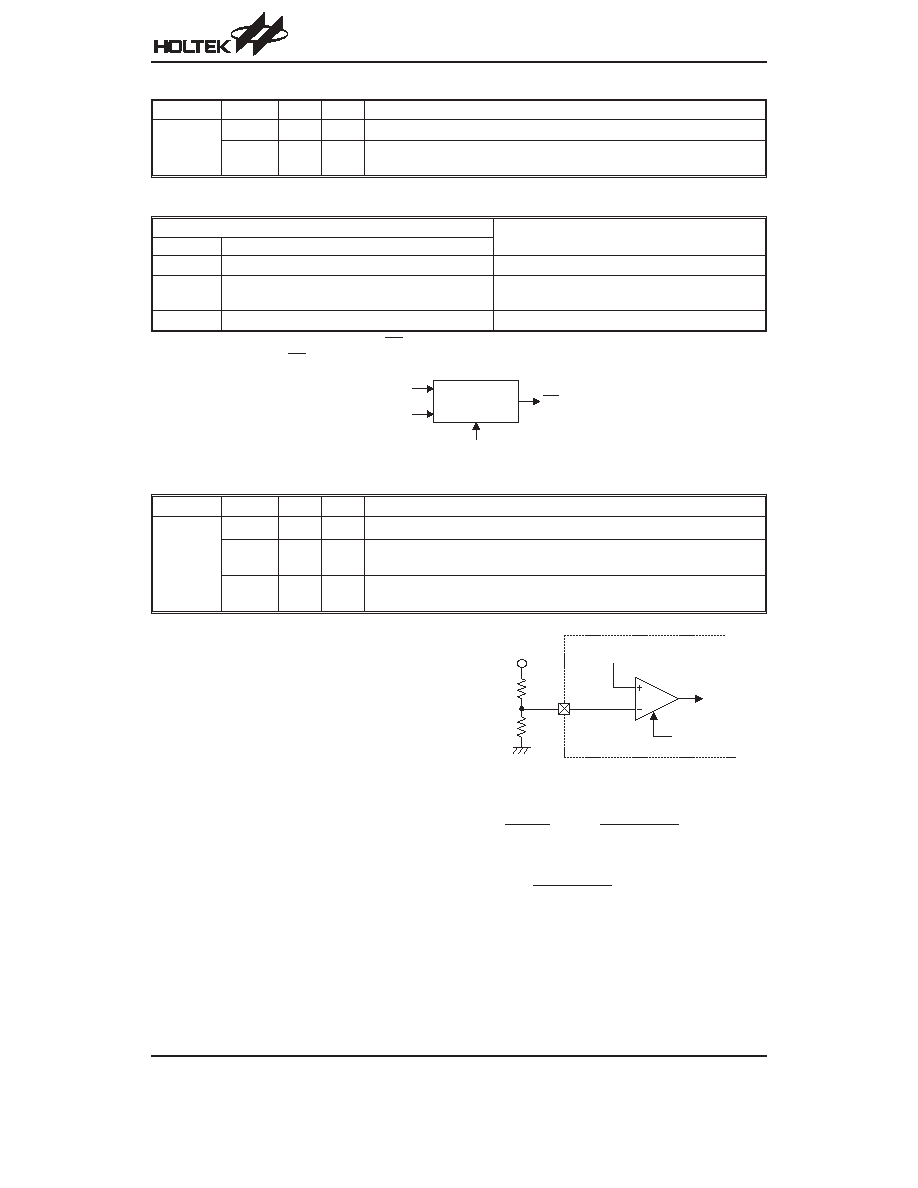
HT95LXXX
Rev. 1.20
27
May 26, 2004
Line Control Function (Supported for HT95L400/40P, HT95L300/30P, HT95L200/20P, HT95L100/10P)
Register
Label
Bits
R/W
Function
LINE
(22H)
ĺ
6~0
RO
Unused bit, read as
≤0≤
LINEC
7
RW
1: Enable the line control function
0: Disable the line control function
The line control function is enabled by flag LINEC
Conditions
Source to Enable
Line Control Function
LINEC
Operation Mode
1
Normal or Green mode
RTC time out interrupt
1
Sleep mode
Port A wake-up
RTC time out interrupt
1
Idle mode
Port A wake-up
When the line control source is activated, the PO pin will be set to high signal. Clearing LINEC to 0 will terminate the line
control function and drive PO pin outputs low signal.
RTC Function
Register
Label
Bits
R/W
Function
RTCC
(24H)
ĺ
6, 4~0
RO
Unused bit, read as
≤0≤
RTCEN
5
RW
1: Enable RTC function
0: Disable RTC function
RTCTO
7
RW
1: RTC time-out occurs
0: RTC time-out not occurs
L i n e C o n t r o l
C i r c u i t
R T C I n t e r r u p t
P o r t A W a k e - u p F u n c t i o n
L I N E C = 1
P O = 1
The real time clock (RTC) is used to supply a regular in-
ternal interrupt. Its time-out period is 1000ms. If the RTC
time-out occurs, the interrupt request flag RTCF and the
RTCTO flag will be set to 1. The interrupt vector for the
RTC is 14H. When the interrupt subroutine is serviced,
the interrupt request flag (RTCF) will be cleared to 0, but
the flag RTCTO remain in its original value. If the
RTCTO flag is not cleared, next RTC time-out interrupt
will occur.
Low Battery Detection
(Supported for HT95L400/40P, HT95L300/30P,
HT95L200/20P, HT95L100/10P)
The phone controller provides a circuit that detects the
LBIN pin voltage level. To enable this detection func-
tion, the LBEN should be written as 1. Once this function
is enabled, the detection circuit needs 50
ms to be stable.
After that, the user could read the result from LBFG. The
low battery detect function will consume power. For
power saving, write 0 to LBEN if the low battery detec-
tion function is unnecessary.
V
D E T
L B I N
L B F G
1 . 1 5 V R e f e r e n c e V o l t a g e
L B E N
R
1
R
2
The battery low threshold is determined by external R1
and R2 resistors.
1.15=
V
xR2
R1+ R2
DET
ģ V
DET
=
1.15x(R1+ R2)
R2
If we want to detect V
DET
=2.4V
then 2.4V=
1.15x(R1+ R2)
R2
ģ R1=1.087R2
HT95LXXX
Rev. 1.20
28
May 26, 2004
LCD Driver
The LCD driver can directly drive an LCD panel with 1/8 duty and 1/4 bias or with 1/16 duty and 1/5 bias, this function is
selected by the flag VBIAS. The frame of this LCD driver may select a 64Hz or 128Hz by flag FRAME.
LCD driver uses the voltage of the VLCD pin as the power source. To adjust the view angle, the programmer can select
the real LCD power by the flags VCON0 and VCON1. The flag LCDON is used to turn On/Off the LCD display. Note that
the VLCD voltage must equal or be less than VDD.
Segment/Common to I/O Selection
For the flexible purpose, some of the LCD COMMON and SEGMENT pins are shared with the input/output port.
Both of the HT95L400/40P and HT95L300/30P provide 12 pins to be selected to SEGMENT output pins or I/O pins.
HT95L200/20P provides 8 pins to be selected for COMMON output pins or I/O pins. Both of the HT95L100/10P and
HT95L000/00P provide 4 pins to be selected for SEGMENT output pins or I/O pins.
All of the HT95L400/40P, HT95L300/30P and HT95L200/20P provide the LCD COMMON output pins for 8 COMMON
or 16 COMMON. The description of the relation between segment pins, common pins and I/O pins are shown on the
below.
Register
Label
Bits R/W
Function
LCDC
(2DH)
FRAME
0
RW
Supported for HT95L400/40P, HT95L300/30P, HT95L200/20P, HT95L100/10P
LCD frame selection
0: LCD frame is 64Hz
1: LCD frame is 128Hz
The frame frequency is fixed to 64Hz for HT95L100/10P and HT95L000/00P
VBIAS
1
RW
Supported for HT95L400/40P, HT95L300/30P, HT95L200/20P
LCD BIAS selection
0: select 1/16 duty and 1/5 bias, COM15~COM0 are available
1: select 1/8 duty and 1/4 bias, only COM15~COM8 are available
When the 8 COM is selected
HT95L400/40P: COM7~COM0 will be optioned to unused pins
HT95L300/30P: COM7~COM0 will be optioned to unused pins
HT95L200/20P: COM7~COM0 are disabled, PD7~PD0 are available
LBEN
2
RW
Supported for HT95L400/40P, HT95L300/30P, HT95L200/20P, HT95L100/10P
Low battery detection switch
0: disable the low battery detection
1: enable the low battery detection
ĺ
3
RO
Unused bit, read as
≤0≤
LBFG
4
ROS
Supported for HT95L400/40P, HT95L300/30P, HT95L200/20P, HT95L100/10P
Low battery detection flag
1: LBIN pin voltage is less than 1.15V
0: LBIN pin voltage is not less than 1.15V
VCON0
VCON1
5
6
RW
LCD contrast adjusting
Bit6,5=00: LCD voltage supply is 0.66
īVLCD
Bit6,5=10: LCD voltage supply is 0.82
īVLCD
Bit6,5=01: LCD voltage supply is 0.93
īVLCD
Bit6,5=11: LCD voltage supply is 1.00
īVLCD
LCDON
7
RW
1: Turn on the LCD display
0: Turn off the LCD display

HT95LXXX
Rev. 1.20
29
May 26, 2004
Register
Label
Bits R/W
Function
LCDIO
(28H)
ĺ
0~4
RO
Unused bit, read as
≤0≤
SPE0
5
RW
Supported for HT95L400/40P, HT95L300/30P, HT95L100/10P, HT95L000/00P
Bit value is 0:
HT95L400/40P: SEG47~SEG44 output are available
HT95L300/30P: SEG47~SEG44 output are available
HT95L100/10P: SEG19~SEG16 output are available
HT95L000/00P: SEG15~SEG12 output are available
Bit value is 1:
HT95L400/40P: PE3~PE0 output are available
HT95L300/30P: PE3~PE0 output are available
HT95L100/10P: PE3~PE0 output are available
HT95L000/00P: PE3~PE0 output are available
SPD0
6
RW
Supported for HT95L400/40P, HT95L300/30P
Bit value is 0: SEG39~SEG36 output are available
Bit value is 1: PD3~PD0 output are available
SPD1
7
RW
Supported for HT95L400/40P, HT95L300/30P
Bit value is 0: SEG43~SEG40 output are available
Bit value is 1: PD7~PD4 output are available
LCD Display Memory
The phone controller provides an area on embedded data memory for LCD display. The LCD display memory are lo-
cated at bank 1BH and can be read and written to, only by indirect addressing mode using MP1. When data is written
into the display data area it is automatically read by the LCD driver which then generates the corresponding LCD driv-
ing signals, to turn the display On or Off, a
≤1≤ or ≤0≤ is written to the corresponding bit of the display memory, respec-
tively. All of the LCD display memories are with random values after the power on reset and unchanged after other reset
conditions.
COM7 to COM0 for HT95L400/40P, HT95L300/30P
Address
Register Name
Bit 7
Bit 6
Bit 5
Bit 4
Bit 3
Bit 2
Bit 1
Bit 0
40H
SEG0
COM7
COM6
COM5
COM4
COM3
COM2
COM1
COM0
41H
SEG1
COM7
COM6
COM5
COM4
COM3
COM2
COM1
COM0
ĺ
ĺ
COM7
COM6
COM5
COM4
COM3
COM2
COM1
COM0
6EH
SEG46
COM7
COM6
COM5
COM4
COM3
COM2
COM1
COM0
6FH
SEG47
COM7
COM6
COM5
COM4
COM3
COM2
COM1
COM0
COM15 to COM8 for HT95L400/40P, HT95L300/30P
Address
Register Name
Bit 7
Bit 6
Bit 5
Bit 4
Bit 3
Bit 2
Bit 1
Bit 0
70H
SEG0
COM15
COM14
COM13
COM12
COM11
COM10
COM9
COM8
71H
SEG1
COM15
COM14
COM13
COM12
COM11
COM10
COM9
COM8
ĺ
ĺ
COM15
COM14
COM13
COM12
COM11
COM10
COM9
COM8
9EH
SEG46
COM15
COM14
COM13
COM12
COM11
COM10
COM9
COM8
9FH
SEG47
COM15
COM14
COM13
COM12
COM11
COM10
COM9
COM8
Note: When VBIAS bit set to 1 for 8 COM operation (48
ī8), the LCD RAM only map to (70H~9FH).

HT95LXXX
Rev. 1.20
30
May 26, 2004
COM7 to COM0 for HT95L200/20P
Address
Register Name
Bit 7
Bit 6
Bit 5
Bit 4
Bit 3
Bit 2
Bit 1
Bit 0
40H
SEG0
COM7
COM6
COM5
COM4
COM3
COM2
COM1
COM0
41H
SEG1
COM7
COM6
COM5
COM4
COM3
COM2
COM1
COM0
ĺ
ĺ
COM7
COM6
COM5
COM4
COM3
COM2
COM1
COM0
56H
SEG22
COM7
COM6
COM5
COM4
COM3
COM2
COM1
COM0
57H
SEG23
COM7
COM6
COM5
COM4
COM3
COM2
COM1
COM0
COM15 to COM8 for HT95L200/20P
Address
Register Name
Bit 7
Bit 6
Bit 5
Bit 4
Bit 3
Bit 2
Bit 1
Bit 0
70H
SEG0
COM15
COM14
COM13
COM12
COM11
COM10
COM9
COM8
71H
SEG1
COM15
COM14
COM13
COM12
COM11
COM10
COM9
COM8
ĺ
ĺ
COM15
COM14
COM13
COM12
COM11
COM10
COM9
COM8
86H
SEG22
COM15
COM14
COM13
COM12
COM11
COM10
COM9
COM8
87H
SEG23
COM15
COM14
COM13
COM12
COM11
COM10
COM9
COM8
Note: When VBIAS bit is set to 1 for 8 COM operation (24
ī8), the LCD RAM only map to (70H~87H).
COM7 to COM0 for HT95L100/10P
Address
Register Name
Bit 7
Bit 6
Bit 5
Bit 4
Bit 3
Bit 2
Bit 1
Bit 0
8CH
SEG0
COM7
COM6
COM5
COM4
COM3
COM2
COM1
COM0
8DH
SEG1
COM7
COM6
COM5
COM4
COM3
COM2
COM1
COM0
ĺ
ĺ
COM7
COM6
COM5
COM4
COM3
COM2
COM1
COM0
9EH
SEG18
COM7
COM6
COM5
COM4
COM3
COM2
COM1
COM0
9FH
SEG19
COM7
COM6
COM5
COM4
COM3
COM2
COM1
COM0
COM7 to COM0 for HT95L000/00P
Address
Register Name
Bit 7
Bit 6
Bit 5
Bit 4
Bit 3
Bit 2
Bit 1
Bit 0
90H
SEG0
COM7
COM6
COM5
COM4
COM3
COM2
COM1
COM0
91H
SEG1
COM7
COM6
COM5
COM4
COM3
COM2
COM1
COM0
ĺ
ĺ
COM7
COM6
COM5
COM4
COM3
COM2
COM1
COM0
9EH
SEG14
COM7
COM6
COM5
COM4
COM3
COM2
COM1
COM0
9FH
SEG15
COM7
COM6
COM5
COM4
COM3
COM2
COM1
COM0
PFD Generator (Supported for HT95L400/40P, HT95L300/30P, HT95L200/20P, HT95L100/10P)
Register
Label
Bits
R/W
Function
PFDC
(2EH)
ĺ
3~0
RO
Unused bit, read as
≤0≤
PFDEN
4
RW
1: Enable PFD output
0: Disable PFD output, the MUSIC pin output low level.
PRES0
PRES1
5
6
RW
Bit6, 5=00: Prescaler output= PFD frequency source/1
Bit6, 5=01: Prescaler output= PFD frequency source/2
Bit6, 5=10: Prescaler output= PFD frequency source/4
Bit6, 5=11: Prescaler output= PFD frequency source/8
FPFD
7
RW
1: The PFD frequency source is 3.58MHz/4
0: The PFD frequency source is 32768Hz
PFDD
(2FH)
ĺ
7~0
RW
PFD data register
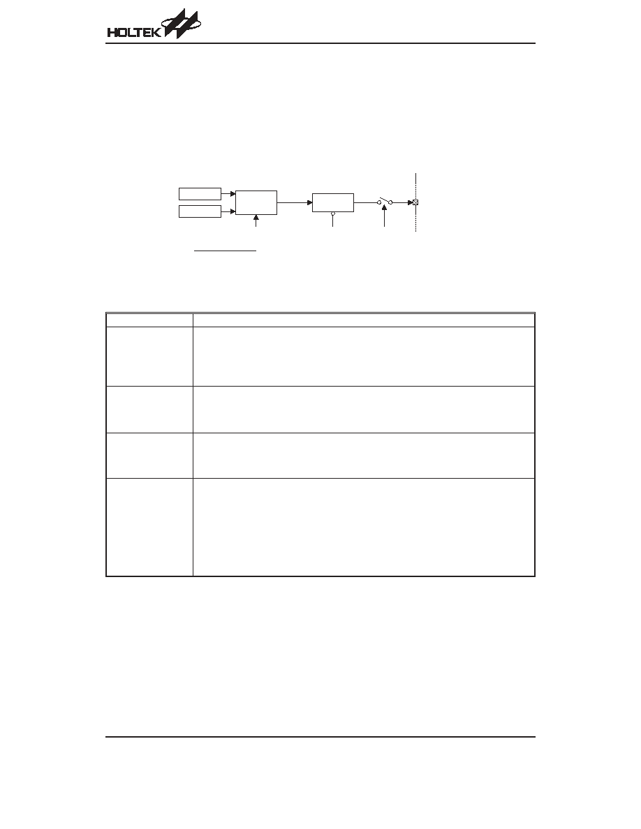
HT95LXXX
Rev. 1.20
31
May 26, 2004
The PFD (programmable frequency divider) is implemented in the phone controller. It is composed of two portions: a
prescaler and a general counter.
The prescaler is controlled by the register bits, PRES0 and PRES1. The general counter is programmed by an 8-bit
register PFDD.
The source for this generator can be selected from 3.58MHz/4 or 32768Hz. To enable the PFD output, write 1 to the
PFDEN bit.
The PFDD is inhibited to write while the PFD is disabled. To modify the PFDD contents, the PFD must be enabled.
When the generator is disabled, the PFDD is cleared by hardware.
PFD output frequency=
Prescaler output
2x(N + 1)
, where N=the value of the PFDD
Mask Option Table
The following shows many kinds of mask options in the telephone controller. All these options should be defined in or-
der to ensure proper system functions.
Name
Mask Option
WDT
WDT source selection
RC
ģSelect the WDT OSC to be the WDT source.
T1
ģSelect the instruction clock to be the WDT source.
32kHz
ģSelect the external 32768Hz to be the WDT source.
Disable
ģDisable WDT function.
CLRWDT
This option defines how to clear the WDT by instruction.
One clear instruction
ģThe ≤CLR WDT≤ can clear the WDT.
Two clear instructions
ģOnly when both of the ≤CLR WDT1≤ and ≤CLR WDT2≤ have been
executed, then WDT can be cleared.
Wake-up PA
Port A wake-up selection.
Define the activity of wake-up function.
All port A have the capability to wake-up the chip from a HALT.
This wake-up function is selected per bit.
Pull-high PA
Pull-high PB
Pull-high PD
Pull-high PE
Pull-high PF
Pull-high PG
Pull-high option.
This option determines whether the pull-high resistance is viable or not.
Port A pull-high option is selected per bit.
Port B pull-high option is selected per bit.
Port D pull-high option is selected per nibble.
(Note: Port D pull-high option is selected per byte for HT95L200/20P.)
Port E pull-high option is selected per nibble.
Port F pull-high option is selected per nibble.
Port G pull-high option is selected per nibble.
P r e s c a l e r
P r e s c a l e r
O u t p u t
P F D D
P R E S 1 , P R E S 0
3 2 7 6 8 H z
3 . 5 8 M H z / 4
P F D E N
P F D
O u t p u t
M U S I C
C l e a r
P F D E N
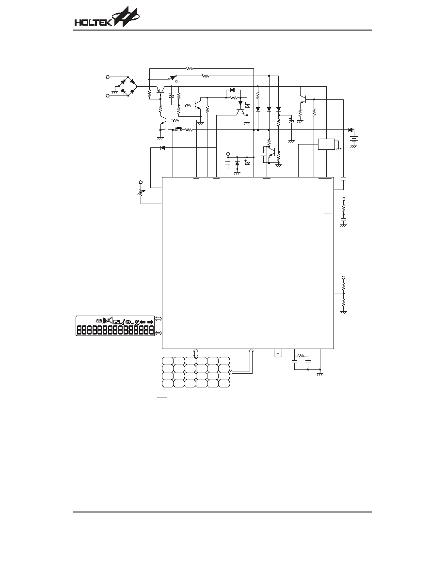
Application Circuits
Note: Some floating input pins (INT/TMR1, TMR0, etc.) are not shown in this circuit.
HT95LXXX
Rev. 1.20
32
May 26, 2004
V
D D
2
5
8
0
3
6
9
#
K e y 1
K e y 2
K e y 3
K e y 4
1
4
7
* / T
V L C D
M E M O R Y
D I A L I N G
S T O R E
H O L D
A M
P M
A B R
M O N
T U E
W E D
T H R
F R I S A T
S U N
C O M M O N
S E G M E N T
X 1
X 2
X C
3 n F
5 0 n F
1 5 k W
3 2 7 6 8 H z
V S S
K e y M a t r i x
L C D P a n n e l
H T 9 5 L X X X
V
D D
1 0 0 k W
0 . 1 m F
R E S
X M U T E
D T M F
S p e e c h
N e t w o r k
V
D D
1 0 0 k W
2 7 0 k W
5 . 1 V
1 0 0 m F
0 . 1 m F
0 . 1 m F
H a n d f r e e
1 . 5 k W
O f f - h o o k
O n - h o o k
1 0 0 k W
R i n g
T i p
2 2 M W
1 0 0 k W
A 9 2
3 . 3 k W
A 4 2
0 . 0 2 m F
H F I
P O
H D I
V D D
H K S
H F O
1 0 0 k W
1 0 m F
2 2 0 k W
3 3 k W
3 3 0 k W
1 N 4 1 4 8
1 m F
2 . 2 k W
2 2 0 k W
1
N
4
1
4
8
1
N
4
1
4
8
1
N
4
1
4
8
4 7 k W
1 m F
1 5 0 k W
M U S I C
I / O
V
D D
L B I N
I / O
I / O
0 . 1 m F
B a t t e r y
1 . 5 ī 3
= 4 . 5 V
1 0 k W
K e y 5
K e y 6
K e y 7
K e y 8
K e y 9
K e y 1 0
K e y 1 1
K e y 1 2
H D O
2 2 0 k W

Instruction Set Summary
Mnemonic
Description
Instruction
Cycle
Flag
Affected
Arithmetic
ADD A,[m]
ADDM A,[m]
ADD A,x
ADC A,[m]
ADCM A,[m]
SUB A,x
SUB A,[m]
SUBM A,[m]
SBC A,[m]
SBCM A,[m]
DAA [m]
Add data memory to ACC
Add ACC to data memory
Add immediate data to ACC
Add data memory to ACC with carry
Add ACC to data memory with carry
Subtract immediate data from ACC
Subtract data memory from ACC
Subtract data memory from ACC with result in data memory
Subtract data memory from ACC with carry
Subtract data memory from ACC with carry and result in data memory
Decimal adjust ACC for addition with result in data memory
1
1
(1)
1
1
1
(1)
1
1
1
(1)
1
1
(1)
1
(1)
Z,C,AC,OV
Z,C,AC,OV
Z,C,AC,OV
Z,C,AC,OV
Z,C,AC,OV
Z,C,AC,OV
Z,C,AC,OV
Z,C,AC,OV
Z,C,AC,OV
Z,C,AC,OV
C
Logic Operation
AND A,[m]
OR A,[m]
XOR A,[m]
ANDM A,[m]
ORM A,[m]
XORM A,[m]
AND A,x
OR A,x
XOR A,x
CPL [m]
CPLA [m]
AND data memory to ACC
OR data memory to ACC
Exclusive-OR data memory to ACC
AND ACC to data memory
OR ACC to data memory
Exclusive-OR ACC to data memory
AND immediate data to ACC
OR immediate data to ACC
Exclusive-OR immediate data to ACC
Complement data memory
Complement data memory with result in ACC
1
1
1
1
(1)
1
(1)
1
(1)
1
1
1
1
(1)
1
Z
Z
Z
Z
Z
Z
Z
Z
Z
Z
Z
Increment & Decrement
INCA [m]
INC [m]
DECA [m]
DEC [m]
Increment data memory with result in ACC
Increment data memory
Decrement data memory with result in ACC
Decrement data memory
1
1
(1)
1
1
(1)
Z
Z
Z
Z
Rotate
RRA [m]
RR [m]
RRCA [m]
RRC [m]
RLA [m]
RL [m]
RLCA [m]
RLC [m]
Rotate data memory right with result in ACC
Rotate data memory right
Rotate data memory right through carry with result in ACC
Rotate data memory right through carry
Rotate data memory left with result in ACC
Rotate data memory left
Rotate data memory left through carry with result in ACC
Rotate data memory left through carry
1
1
(1)
1
1
(1)
1
1
(1)
1
1
(1)
None
None
C
C
None
None
C
C
Data Move
MOV A,[m]
MOV [m],A
MOV A,x
Move data memory to ACC
Move ACC to data memory
Move immediate data to ACC
1
1
(1)
1
None
None
None
Bit Operation
CLR [m].i
SET [m].i
Clear bit of data memory
Set bit of data memory
1
(1)
1
(1)
None
None
HT95LXXX
Rev. 1.20
33
May 26, 2004

Mnemonic
Description
Instruction
Cycle
Flag
Affected
Branch
JMP addr
SZ [m]
SZA [m]
SZ [m].i
SNZ [m].i
SIZ [m]
SDZ [m]
SIZA [m]
SDZA [m]
CALL addr
RET
RET A,x
RETI
Jump unconditionally
Skip if data memory is zero
Skip if data memory is zero with data movement to ACC
Skip if bit i of data memory is zero
Skip if bit i of data memory is not zero
Skip if increment data memory is zero
Skip if decrement data memory is zero
Skip if increment data memory is zero with result in ACC
Skip if decrement data memory is zero with result in ACC
Subroutine call
Return from subroutine
Return from subroutine and load immediate data to ACC
Return from interrupt
2
1
(2)
1
(2)
1
(2)
1
(2)
1
(3)
1
(3)
1
(2)
1
(2)
2
2
2
2
None
None
None
None
None
None
None
None
None
None
None
None
None
Table Read
TABRDC [m]
TABRDL [m]
Read ROM code (current page) to data memory and TBLH
Read ROM code (last page) to data memory and TBLH
2
(1)
2
(1)
None
None
Miscellaneous
NOP
CLR [m]
SET [m]
CLR WDT
CLR WDT1
CLR WDT2
SWAP [m]
SWAPA [m]
HALT
No operation
Clear data memory
Set data memory
Clear Watchdog Timer
Pre-clear Watchdog Timer
Pre-clear Watchdog Timer
Swap nibbles of data memory
Swap nibbles of data memory with result in ACC
Enter power down mode
1
1
(1)
1
(1)
1
1
1
1
(1)
1
1
None
None
None
TO,PDF
TO
(4)
,PDF
(4)
TO
(4)
,PDF
(4)
None
None
TO,PDF
Note: x: Immediate data
m: Data memory address
A: Accumulator
i: 0~7 number of bits
addr: Program memory address
÷: Flag is affected
-: Flag is not affected
(1)
: If a loading to the PCL register occurs, the execution cycle of instructions will be delayed for one more cycle
(four system clocks).
(2)
: If a skipping to the next instruction occurs, the execution cycle of instructions will be delayed for one more
cycle (four system clocks). Otherwise the original instruction cycle is unchanged.
(3)
:
(1)
and
(2)
(4)
: The flags may be affected by the execution status. If the Watchdog Timer is cleared by executing the
≤CLR WDT1≤ or ≤CLR WDT2≤ instruction, the TO and PDF are cleared.
Otherwise the TO and PDF flags remain unchanged.
HT95LXXX
Rev. 1.20
34
May 26, 2004

Instruction Definition
ADC A,[m]
Add data memory and carry to the accumulator
Description
The contents of the specified data memory, accumulator and the carry flag are added si-
multaneously, leaving the result in the accumulator.
Operation
ACC
¨ ACC+[m]+C
Affected flag(s)
TO
PDF
OV
Z
AC
C
ĺ
ĺ
÷
÷
÷
÷
ADCM A,[m]
Add the accumulator and carry to data memory
Description
The contents of the specified data memory, accumulator and the carry flag are added si-
multaneously, leaving the result in the specified data memory.
Operation
[m]
¨ ACC+[m]+C
Affected flag(s)
TO
PDF
OV
Z
AC
C
ĺ
ĺ
÷
÷
÷
÷
ADD A,[m]
Add data memory to the accumulator
Description
The contents of the specified data memory and the accumulator are added. The result is
stored in the accumulator.
Operation
ACC
¨ ACC+[m]
Affected flag(s)
TO
PDF
OV
Z
AC
C
ĺ
ĺ
÷
÷
÷
÷
ADD A,x
Add immediate data to the accumulator
Description
The contents of the accumulator and the specified data are added, leaving the result in the
accumulator.
Operation
ACC
¨ ACC+x
Affected flag(s)
TO
PDF
OV
Z
AC
C
ĺ
ĺ
÷
÷
÷
÷
ADDM A,[m]
Add the accumulator to the data memory
Description
The contents of the specified data memory and the accumulator are added. The result is
stored in the data memory.
Operation
[m]
¨ ACC+[m]
Affected flag(s)
TO
PDF
OV
Z
AC
C
ĺ
ĺ
÷
÷
÷
÷
HT95LXXX
Rev. 1.20
35
May 26, 2004

AND A,[m]
Logical AND accumulator with data memory
Description
Data in the accumulator and the specified data memory perform a bitwise logical_AND op-
eration. The result is stored in the accumulator.
Operation
ACC
¨ ACC ≤AND≤ [m]
Affected flag(s)
TO
PDF
OV
Z
AC
C
ĺ
ĺ
ĺ
÷
ĺ
ĺ
AND A,x
Logical AND immediate data to the accumulator
Description
Data in the accumulator and the specified data perform a bitwise logical_AND operation.
The result is stored in the accumulator.
Operation
ACC
¨ ACC ≤AND≤ x
Affected flag(s)
TO
PDF
OV
Z
AC
C
ĺ
ĺ
ĺ
÷
ĺ
ĺ
ANDM A,[m]
Logical AND data memory with the accumulator
Description
Data in the specified data memory and the accumulator perform a bitwise logical_AND op-
eration. The result is stored in the data memory.
Operation
[m]
¨ ACC ≤AND≤ [m]
Affected flag(s)
TO
PDF
OV
Z
AC
C
ĺ
ĺ
ĺ
÷
ĺ
ĺ
CALL addr
Subroutine call
Description
The instruction unconditionally calls a subroutine located at the indicated address. The
program counter increments once to obtain the address of the next instruction, and pushes
this onto the stack. The indicated address is then loaded. Program execution continues
with the instruction at this address.
Operation
Stack
¨ PC+1
PC
¨ addr
Affected flag(s)
TO
PDF
OV
Z
AC
C
ĺ
ĺ
ĺ
ĺ
ĺ
ĺ
CLR [m]
Clear data memory
Description
The contents of the specified data memory are cleared to 0.
Operation
[m]
¨ 00H
Affected flag(s)
TO
PDF
OV
Z
AC
C
ĺ
ĺ
ĺ
ĺ
ĺ
ĺ
HT95LXXX
Rev. 1.20
36
May 26, 2004

CLR [m].i
Clear bit of data memory
Description
The bit i of the specified data memory is cleared to 0.
Operation
[m].i
¨ 0
Affected flag(s)
TO
PDF
OV
Z
AC
C
ĺ
ĺ
ĺ
ĺ
ĺ
ĺ
CLR WDT
Clear Watchdog Timer
Description
The WDT is cleared (clears the WDT). The power down bit (PDF) and time-out bit (TO) are
cleared.
Operation
WDT
¨ 00H
PDF and TO
¨ 0
Affected flag(s)
TO
PDF
OV
Z
AC
C
0
0
ĺ
ĺ
ĺ
ĺ
CLR WDT1
Preclear Watchdog Timer
Description
Together with CLR WDT2, clears the WDT. PDF and TO are also cleared. Only execution
of this instruction without the other preclear instruction just sets the indicated flag which im-
plies this instruction has been executed and the TO and PDF flags remain unchanged.
Operation
WDT
¨ 00H*
PDF and TO
¨ 0*
Affected flag(s)
TO
PDF
OV
Z
AC
C
0*
0*
ĺ
ĺ
ĺ
ĺ
CLR WDT2
Preclear Watchdog Timer
Description
Together with CLR WDT1, clears the WDT. PDF and TO are also cleared. Only execution
of this instruction without the other preclear instruction, sets the indicated flag which im-
plies this instruction has been executed and the TO and PDF flags remain unchanged.
Operation
WDT
¨ 00H*
PDF and TO
¨ 0*
Affected flag(s)
TO
PDF
OV
Z
AC
C
0*
0*
ĺ
ĺ
ĺ
ĺ
CPL [m]
Complement data memory
Description
Each bit of the specified data memory is logically complemented (1
Ęs complement). Bits
which previously contained a 1 are changed to 0 and vice-versa.
Operation
[m]
¨ [m]
Affected flag(s)
TO
PDF
OV
Z
AC
C
ĺ
ĺ
ĺ
÷
ĺ
ĺ
HT95LXXX
Rev. 1.20
37
May 26, 2004

CPLA [m]
Complement data memory and place result in the accumulator
Description
Each bit of the specified data memory is logically complemented (1
Ęs complement). Bits
which previously contained a 1 are changed to 0 and vice-versa. The complemented result
is stored in the accumulator and the contents of the data memory remain unchanged.
Operation
ACC
¨ [m]
Affected flag(s)
TO
PDF
OV
Z
AC
C
ĺ
ĺ
ĺ
÷
ĺ
ĺ
DAA [m]
Decimal-Adjust accumulator for addition
Description
The accumulator value is adjusted to the BCD (Binary Coded Decimal) code. The accumu-
lator is divided into two nibbles. Each nibble is adjusted to the BCD code and an internal
carry (AC1) will be done if the low nibble of the accumulator is greater than 9. The BCD ad-
justment is done by adding 6 to the original value if the original value is greater than 9 or a
carry (AC or C) is set; otherwise the original value remains unchanged. The result is stored
in the data memory and only the carry flag (C) may be affected.
Operation
If ACC.3~ACC.0 >9 or AC=1
then [m].3~[m].0
¨ (ACC.3~ACC.0)+6, AC1=AC
else [m].3~[m].0
¨ (ACC.3~ACC.0), AC1=0
and
If ACC.7~ACC.4+AC1 >9 or C=1
then [m].7~[m].4
¨ ACC.7~ACC.4+6+AC1,C=1
else [m].7~[m].4
¨ ACC.7~ACC.4+AC1,C=C
Affected flag(s)
TO
PDF
OV
Z
AC
C
ĺ
ĺ
ĺ
ĺ
ĺ
÷
DEC [m]
Decrement data memory
Description
Data in the specified data memory is decremented by 1.
Operation
[m]
¨ [m]-1
Affected flag(s)
TO
PDF
OV
Z
AC
C
ĺ
ĺ
ĺ
÷
ĺ
ĺ
DECA [m]
Decrement data memory and place result in the accumulator
Description
Data in the specified data memory is decremented by 1, leaving the result in the accumula-
tor. The contents of the data memory remain unchanged.
Operation
ACC
¨ [m]-1
Affected flag(s)
TO
PDF
OV
Z
AC
C
ĺ
ĺ
ĺ
÷
ĺ
ĺ
HT95LXXX
Rev. 1.20
38
May 26, 2004

HALT
Enter power down mode
Description
This instruction stops program execution and turns off the system clock. The contents of
the RAM and registers are retained. The WDT and prescaler are cleared. The power down
bit (PDF) is set and the WDT time-out bit (TO) is cleared.
Operation
PC
¨ PC+1
PDF
¨ 1
TO
¨ 0
Affected flag(s)
TO
PDF
OV
Z
AC
C
0
1
ĺ
ĺ
ĺ
ĺ
INC [m]
Increment data memory
Description
Data in the specified data memory is incremented by 1
Operation
[m]
¨ [m]+1
Affected flag(s)
TO
PDF
OV
Z
AC
C
ĺ
ĺ
ĺ
÷
ĺ
ĺ
INCA [m]
Increment data memory and place result in the accumulator
Description
Data in the specified data memory is incremented by 1, leaving the result in the accumula-
tor. The contents of the data memory remain unchanged.
Operation
ACC
¨ [m]+1
Affected flag(s)
TO
PDF
OV
Z
AC
C
ĺ
ĺ
ĺ
÷
ĺ
ĺ
JMP addr
Directly jump
Description
The program counter are replaced with the directly-specified address unconditionally, and
control is passed to this destination.
Operation
PC
¨addr
Affected flag(s)
TO
PDF
OV
Z
AC
C
ĺ
ĺ
ĺ
ĺ
ĺ
ĺ
MOV A,[m]
Move data memory to the accumulator
Description
The contents of the specified data memory are copied to the accumulator.
Operation
ACC
¨ [m]
Affected flag(s)
TO
PDF
OV
Z
AC
C
ĺ
ĺ
ĺ
ĺ
ĺ
ĺ
HT95LXXX
Rev. 1.20
39
May 26, 2004

MOV A,x
Move immediate data to the accumulator
Description
The 8-bit data specified by the code is loaded into the accumulator.
Operation
ACC
¨ x
Affected flag(s)
TO
PDF
OV
Z
AC
C
ĺ
ĺ
ĺ
ĺ
ĺ
ĺ
MOV [m],A
Move the accumulator to data memory
Description
The contents of the accumulator are copied to the specified data memory (one of the data
memories).
Operation
[m]
¨ACC
Affected flag(s)
TO
PDF
OV
Z
AC
C
ĺ
ĺ
ĺ
ĺ
ĺ
ĺ
NOP
No operation
Description
No operation is performed. Execution continues with the next instruction.
Operation
PC
¨ PC+1
Affected flag(s)
TO
PDF
OV
Z
AC
C
ĺ
ĺ
ĺ
ĺ
ĺ
ĺ
OR A,[m]
Logical OR accumulator with data memory
Description
Data in the accumulator and the specified data memory (one of the data memories) per-
form a bitwise logical_OR operation. The result is stored in the accumulator.
Operation
ACC
¨ ACC ≤OR≤ [m]
Affected flag(s)
TO
PDF
OV
Z
AC
C
ĺ
ĺ
ĺ
÷
ĺ
ĺ
OR A,x
Logical OR immediate data to the accumulator
Description
Data in the accumulator and the specified data perform a bitwise logical_OR operation.
The result is stored in the accumulator.
Operation
ACC
¨ ACC ≤OR≤ x
Affected flag(s)
TO
PDF
OV
Z
AC
C
ĺ
ĺ
ĺ
÷
ĺ
ĺ
ORM A,[m]
Logical OR data memory with the accumulator
Description
Data in the data memory (one of the data memories) and the accumulator perform a
bitwise logical_OR operation. The result is stored in the data memory.
Operation
[m]
¨ACC ≤OR≤ [m]
Affected flag(s)
TO
PDF
OV
Z
AC
C
ĺ
ĺ
ĺ
÷
ĺ
ĺ
HT95LXXX
Rev. 1.20
40
May 26, 2004

RET
Return from subroutine
Description
The program counter is restored from the stack. This is a 2-cycle instruction.
Operation
PC
¨ Stack
Affected flag(s)
TO
PDF
OV
Z
AC
C
ĺ
ĺ
ĺ
ĺ
ĺ
ĺ
RET A,x
Return and place immediate data in the accumulator
Description
The program counter is restored from the stack and the accumulator loaded with the speci-
fied 8-bit immediate data.
Operation
PC
¨ Stack
ACC
¨ x
Affected flag(s)
TO
PDF
OV
Z
AC
C
ĺ
ĺ
ĺ
ĺ
ĺ
ĺ
RETI
Return from interrupt
Description
The program counter is restored from the stack, and interrupts are enabled by setting the
EMI bit. EMI is the enable master (global) interrupt bit.
Operation
PC
¨ Stack
EMI
¨ 1
Affected flag(s)
TO
PDF
OV
Z
AC
C
ĺ
ĺ
ĺ
ĺ
ĺ
ĺ
RL [m]
Rotate data memory left
Description
The contents of the specified data memory are rotated 1 bit left with bit 7 rotated into bit 0.
Operation
[m].(i+1)
¨ [m].i; [m].i:bit i of the data memory (i=0~6)
[m].0
¨ [m].7
Affected flag(s)
TO
PDF
OV
Z
AC
C
ĺ
ĺ
ĺ
ĺ
ĺ
ĺ
RLA [m]
Rotate data memory left and place result in the accumulator
Description
Data in the specified data memory is rotated 1 bit left with bit 7 rotated into bit 0, leaving the
rotated result in the accumulator. The contents of the data memory remain unchanged.
Operation
ACC.(i+1)
¨ [m].i; [m].i:bit i of the data memory (i=0~6)
ACC.0
¨ [m].7
Affected flag(s)
TO
PDF
OV
Z
AC
C
ĺ
ĺ
ĺ
ĺ
ĺ
ĺ
HT95LXXX
Rev. 1.20
41
May 26, 2004
RLC [m]
Rotate data memory left through carry
Description
The contents of the specified data memory and the carry flag are rotated 1 bit left. Bit 7 re-
places the carry bit; the original carry flag is rotated into the bit 0 position.
Operation
[m].(i+1)
¨ [m].i; [m].i:bit i of the data memory (i=0~6)
[m].0
¨ C
C
¨ [m].7
Affected flag(s)
TO
PDF
OV
Z
AC
C
ĺ
ĺ
ĺ
ĺ
ĺ
÷
RLCA [m]
Rotate left through carry and place result in the accumulator
Description
Data in the specified data memory and the carry flag are rotated 1 bit left. Bit 7 replaces the
carry bit and the original carry flag is rotated into bit 0 position. The rotated result is stored
in the accumulator but the contents of the data memory remain unchanged.
Operation
ACC.(i+1)
¨ [m].i; [m].i:bit i of the data memory (i=0~6)
ACC.0
¨ C
C
¨ [m].7
Affected flag(s)
TO
PDF
OV
Z
AC
C
ĺ
ĺ
ĺ
ĺ
ĺ
÷
RR [m]
Rotate data memory right
Description
The contents of the specified data memory are rotated 1 bit right with bit 0 rotated to bit 7.
Operation
[m].i
¨ [m].(i+1); [m].i:bit i of the data memory (i=0~6)
[m].7
¨ [m].0
Affected flag(s)
TO
PDF
OV
Z
AC
C
ĺ
ĺ
ĺ
ĺ
ĺ
ĺ
RRA [m]
Rotate right and place result in the accumulator
Description
Data in the specified data memory is rotated 1 bit right with bit 0 rotated into bit 7, leaving
the rotated result in the accumulator. The contents of the data memory remain unchanged.
Operation
ACC.(i)
¨ [m].(i+1); [m].i:bit i of the data memory (i=0~6)
ACC.7
¨ [m].0
Affected flag(s)
TO
PDF
OV
Z
AC
C
ĺ
ĺ
ĺ
ĺ
ĺ
ĺ
RRC [m]
Rotate data memory right through carry
Description
The contents of the specified data memory and the carry flag are together rotated 1 bit
right. Bit 0 replaces the carry bit; the original carry flag is rotated into the bit 7 position.
Operation
[m].i
¨ [m].(i+1); [m].i:bit i of the data memory (i=0~6)
[m].7
¨ C
C
¨ [m].0
Affected flag(s)
TO
PDF
OV
Z
AC
C
ĺ
ĺ
ĺ
ĺ
ĺ
÷
HT95LXXX
Rev. 1.20
42
May 26, 2004
RRCA [m]
Rotate right through carry and place result in the accumulator
Description
Data of the specified data memory and the carry flag are rotated 1 bit right. Bit 0 replaces
the carry bit and the original carry flag is rotated into the bit 7 position. The rotated result is
stored in the accumulator. The contents of the data memory remain unchanged.
Operation
ACC.i
¨ [m].(i+1); [m].i:bit i of the data memory (i=0~6)
ACC.7
¨ C
C
¨ [m].0
Affected flag(s)
TO
PDF
OV
Z
AC
C
ĺ
ĺ
ĺ
ĺ
ĺ
÷
SBC A,[m]
Subtract data memory and carry from the accumulator
Description
The contents of the specified data memory and the complement of the carry flag are sub-
tracted from the accumulator, leaving the result in the accumulator.
Operation
ACC
¨ ACC+[m]+C
Affected flag(s)
TO
PDF
OV
Z
AC
C
ĺ
ĺ
÷
÷
÷
÷
SBCM A,[m]
Subtract data memory and carry from the accumulator
Description
The contents of the specified data memory and the complement of the carry flag are sub-
tracted from the accumulator, leaving the result in the data memory.
Operation
[m]
¨ ACC+[m]+C
Affected flag(s)
TO
PDF
OV
Z
AC
C
ĺ
ĺ
÷
÷
÷
÷
SDZ [m]
Skip if decrement data memory is 0
Description
The contents of the specified data memory are decremented by 1. If the result is 0, the next
instruction is skipped. If the result is 0, the following instruction, fetched during the current
instruction execution, is discarded and a dummy cycle is replaced to get the proper instruc-
tion (2 cycles). Otherwise proceed with the next instruction (1 cycle).
Operation
Skip if ([m]
-1)=0, [m] ¨ ([m]-1)
Affected flag(s)
TO
PDF
OV
Z
AC
C
ĺ
ĺ
ĺ
ĺ
ĺ
ĺ
SDZA [m]
Decrement data memory and place result in ACC, skip if 0
Description
The contents of the specified data memory are decremented by 1. If the result is 0, the next
instruction is skipped. The result is stored in the accumulator but the data memory remains
unchanged. If the result is 0, the following instruction, fetched during the current instruction
execution, is discarded and a dummy cycle is replaced to get the proper instruction (2 cy-
cles). Otherwise proceed with the next instruction (1 cycle).
Operation
Skip if ([m]
-1)=0, ACC ¨ ([m]-1)
Affected flag(s)
TO
PDF
OV
Z
AC
C
ĺ
ĺ
ĺ
ĺ
ĺ
ĺ
HT95LXXX
Rev. 1.20
43
May 26, 2004

SET [m]
Set data memory
Description
Each bit of the specified data memory is set to 1.
Operation
[m]
¨ FFH
Affected flag(s)
TO
PDF
OV
Z
AC
C
ĺ
ĺ
ĺ
ĺ
ĺ
ĺ
SET [m]. i
Set bit of data memory
Description
Bit i of the specified data memory is set to 1.
Operation
[m].i
¨ 1
Affected flag(s)
TO
PDF
OV
Z
AC
C
ĺ
ĺ
ĺ
ĺ
ĺ
ĺ
SIZ [m]
Skip if increment data memory is 0
Description
The contents of the specified data memory are incremented by 1. If the result is 0, the fol-
lowing instruction, fetched during the current instruction execution, is discarded and a
dummy cycle is replaced to get the proper instruction (2 cycles). Otherwise proceed with
the next instruction (1 cycle).
Operation
Skip if ([m]+1)=0, [m]
¨ ([m]+1)
Affected flag(s)
TO
PDF
OV
Z
AC
C
ĺ
ĺ
ĺ
ĺ
ĺ
ĺ
SIZA [m]
Increment data memory and place result in ACC, skip if 0
Description
The contents of the specified data memory are incremented by 1. If the result is 0, the next
instruction is skipped and the result is stored in the accumulator. The data memory re-
mains unchanged. If the result is 0, the following instruction, fetched during the current in-
struction execution, is discarded and a dummy cycle is replaced to get the proper
instruction (2 cycles). Otherwise proceed with the next instruction (1 cycle).
Operation
Skip if ([m]+1)=0, ACC
¨ ([m]+1)
Affected flag(s)
TO
PDF
OV
Z
AC
C
ĺ
ĺ
ĺ
ĺ
ĺ
ĺ
SNZ [m].i
Skip if bit i of the data memory is not 0
Description
If bit i of the specified data memory is not 0, the next instruction is skipped. If bit i of the data
memory is not 0, the following instruction, fetched during the current instruction execution,
is discarded and a dummy cycle is replaced to get the proper instruction (2 cycles). Other-
wise proceed with the next instruction (1 cycle).
Operation
Skip if [m].i
Ļ0
Affected flag(s)
TO
PDF
OV
Z
AC
C
ĺ
ĺ
ĺ
ĺ
ĺ
ĺ
HT95LXXX
Rev. 1.20
44
May 26, 2004

SUB A,[m]
Subtract data memory from the accumulator
Description
The specified data memory is subtracted from the contents of the accumulator, leaving the
result in the accumulator.
Operation
ACC
¨ ACC+[m]+1
Affected flag(s)
TO
PDF
OV
Z
AC
C
ĺ
ĺ
÷
÷
÷
÷
SUBM A,[m]
Subtract data memory from the accumulator
Description
The specified data memory is subtracted from the contents of the accumulator, leaving the
result in the data memory.
Operation
[m]
¨ ACC+[m]+1
Affected flag(s)
TO
PDF
OV
Z
AC
C
ĺ
ĺ
÷
÷
÷
÷
SUB A,x
Subtract immediate data from the accumulator
Description
The immediate data specified by the code is subtracted from the contents of the accumula-
tor, leaving the result in the accumulator.
Operation
ACC
¨ ACC+x+1
Affected flag(s)
TO
PDF
OV
Z
AC
C
ĺ
ĺ
÷
÷
÷
÷
SWAP [m]
Swap nibbles within the data memory
Description
The low-order and high-order nibbles of the specified data memory (1 of the data memo-
ries) are interchanged.
Operation
[m].3~[m].0
ę [m].7~[m].4
Affected flag(s)
TO
PDF
OV
Z
AC
C
ĺ
ĺ
ĺ
ĺ
ĺ
ĺ
SWAPA [m]
Swap data memory and place result in the accumulator
Description
The low-order and high-order nibbles of the specified data memory are interchanged, writ-
ing the result to the accumulator. The contents of the data memory remain unchanged.
Operation
ACC.3~ACC.0
¨ [m].7~[m].4
ACC.7~ACC.4
¨ [m].3~[m].0
Affected flag(s)
TO
PDF
OV
Z
AC
C
ĺ
ĺ
ĺ
ĺ
ĺ
ĺ
HT95LXXX
Rev. 1.20
45
May 26, 2004
SZ [m]
Skip if data memory is 0
Description
If the contents of the specified data memory are 0, the following instruction, fetched during
the current instruction execution, is discarded and a dummy cycle is replaced to get the
proper instruction (2 cycles). Otherwise proceed with the next instruction (1 cycle).
Operation
Skip if [m]=0
Affected flag(s)
TO
PDF
OV
Z
AC
C
ĺ
ĺ
ĺ
ĺ
ĺ
ĺ
SZA [m]
Move data memory to ACC, skip if 0
Description
The contents of the specified data memory are copied to the accumulator. If the contents is
0, the following instruction, fetched during the current instruction execution, is discarded
and a dummy cycle is replaced to get the proper instruction (2 cycles). Otherwise proceed
with the next instruction (1 cycle).
Operation
Skip if [m]=0
Affected flag(s)
TO
PDF
OV
Z
AC
C
ĺ
ĺ
ĺ
ĺ
ĺ
ĺ
SZ [m].i
Skip if bit i of the data memory is 0
Description
If bit i of the specified data memory is 0, the following instruction, fetched during the current
instruction execution, is discarded and a dummy cycle is replaced to get the proper instruc-
tion (2 cycles). Otherwise proceed with the next instruction (1 cycle).
Operation
Skip if [m].i=0
Affected flag(s)
TO
PDF
OV
Z
AC
C
ĺ
ĺ
ĺ
ĺ
ĺ
ĺ
TABRDC [m]
Move the ROM code (current page) to TBLH and data memory
Description
The low byte of ROM code (current page) addressed by the table pointer (TBLP) is moved
to the specified data memory and the high byte transferred to TBLH directly.
Operation
[m]
¨ ROM code (low byte)
TBLH
¨ ROM code (high byte)
Affected flag(s)
TO
PDF
OV
Z
AC
C
ĺ
ĺ
ĺ
ĺ
ĺ
ĺ
TABRDL [m]
Move the ROM code (last page) to TBLH and data memory
Description
The low byte of ROM code (last page) addressed by the table pointer (TBLP) is moved to
the data memory and the high byte transferred to TBLH directly.
Operation
[m]
¨ ROM code (low byte)
TBLH
¨ ROM code (high byte)
Affected flag(s)
TO
PDF
OV
Z
AC
C
ĺ
ĺ
ĺ
ĺ
ĺ
ĺ
HT95LXXX
Rev. 1.20
46
May 26, 2004

XOR A,[m]
Logical XOR accumulator with data memory
Description
Data in the accumulator and the indicated data memory perform a bitwise logical Exclu-
sive_OR operation and the result is stored in the accumulator.
Operation
ACC
¨ ACC ≤XOR≤ [m]
Affected flag(s)
TO
PDF
OV
Z
AC
C
ĺ
ĺ
ĺ
÷
ĺ
ĺ
XORM A,[m]
Logical XOR data memory with the accumulator
Description
Data in the indicated data memory and the accumulator perform a bitwise logical Exclu-
sive_OR operation. The result is stored in the data memory. The 0 flag is affected.
Operation
[m]
¨ ACC ≤XOR≤ [m]
Affected flag(s)
TO
PDF
OV
Z
AC
C
ĺ
ĺ
ĺ
÷
ĺ
ĺ
XOR A,x
Logical XOR immediate data to the accumulator
Description
Data in the accumulator and the specified data perform a bitwise logical Exclusive_OR op-
eration. The result is stored in the accumulator. The 0 flag is affected.
Operation
ACC
¨ ACC ≤XOR≤ x
Affected flag(s)
TO
PDF
OV
Z
AC
C
ĺ
ĺ
ĺ
÷
ĺ
ĺ
HT95LXXX
Rev. 1.20
47
May 26, 2004

Package Information
56-pin SSOP (300mil) Outline Dimensions
Symbol
Dimensions in mil
Min.
Nom.
Max.
A
395
ĺ
420
B
291
ĺ
299
C
8
ĺ
12
C
Ę
720
ĺ
730
D
89
ĺ
99
E
ĺ
25
ĺ
F
4
ĺ
10
G
25
ĺ
35
H
4
ĺ
12
a
0
į
ĺ
8
į
HT95LXXX
Rev. 1.20
48
May 26, 2004
5 6
1
A
2 9
2 8
B
C
D
F
C '
H
a
E
G

64-pin QFP (14
ī20) Outline Dimensions
Symbol
Dimensions in mm
Min.
Nom.
Max.
A
18.80
ĺ
19.20
B
13.90
ĺ
14.10
C
24.80
ĺ
25.20
D
19.90
ĺ
20.10
E
ĺ
1
ĺ
F
ĺ
0.40
ĺ
G
2.50
ĺ
3.10
H
ĺ
ĺ
3.40
I
ĺ
0.10
ĺ
J
1.15
ĺ
1.45
K
0.10
ĺ
0.20
a
0
į
ĺ
7
į
HT95LXXX
Rev. 1.20
49
May 26, 2004
5 1
5 2
6 4
1
2 0
3 2
3 3
1 9
A
B
C
D
E
F
G
H
I
J
K
a

100-pin QFP (14
ī20) Outline Dimensions
Symbol
Dimensions in mm
Min.
Nom.
Max.
A
18.50
ĺ
19.20
B
13.90
ĺ
14.10
C
24.50
ĺ
25.20
D
19.90
ĺ
20.10
E
ĺ
0.65
ĺ
F
ĺ
0.30
ĺ
G
2.50
ĺ
3.10
H
ĺ
ĺ
3.40
I
ĺ
0.10
ĺ
J
1
ĺ
1.40
K
0.10
ĺ
0.20
a
0
į
ĺ
7
į
HT95LXXX
Rev. 1.20
50
May 26, 2004
1 0 0
8 1
8 0
5 1
5 0
3 1
3 0
1
A
B
C
D
E
F
G
H
I
J
K
a

128-pin QFP (14
ī20) Outline Dimensions
Symbol
Dimensions in mm
Min.
Nom.
Max.
A
17.00
ĺ
17.50
B
13.90
ĺ
14.10
C
23.00
ĺ
23.50
D
19.90
ĺ
20.10
E
ĺ
0.50
ĺ
F
ĺ
0.20
ĺ
G
2.50
ĺ
3.10
H
ĺ
ĺ
3.40
I
ĺ
0.10
ĺ
J
0.65
ĺ
0.95
K
0.10
ĺ
0.20
a
0
į
ĺ
7
į
HT95LXXX
Rev. 1.20
51
May 26, 2004
1 0 3
1 2 8
1
3 8
3 9
A
B
1 0 2
6 5
C
D
E
F
G
H
I
J
K
a
6 4

HT95LXXX
Rev. 1.20
52
May 26, 2004
Copyright
” 2004 by HOLTEK SEMICONDUCTOR INC.
The information appearing in this Data Sheet is believed to be accurate at the time of publication. However, Holtek as-
sumes no responsibility arising from the use of the specifications described. The applications mentioned herein are used
solely for the purpose of illustration and Holtek makes no warranty or representation that such applications will be suitable
without further modification, nor recommends the use of its products for application that may present a risk to human life
due to malfunction or otherwise. Holtek
Ęs products are not authorized for use as critical components in life support devices
or systems. Holtek reserves the right to alter its products without prior notification. For the most up-to-date information,
please visit our web site at http://www.holtek.com.tw.
Holtek Semiconductor Inc. (Headquarters)
No.3, Creation Rd. II, Science Park, Hsinchu, Taiwan
Tel: 886-3-563-1999
Fax: 886-3-563-1189
http://www.holtek.com.tw
Holtek Semiconductor Inc. (Taipei Sales Office)
4F-2, No. 3-2, YuanQu St., Nankang Software Park, Taipei 115, Taiwan
Tel: 886-2-2655-7070
Fax: 886-2-2655-7373
Fax: 886-2-2655-7383 (International sales hotline)
Holtek Semiconductor Inc. (Shanghai Sales Office)
7th Floor, Building 2, No.889, Yi Shan Rd., Shanghai, China 200233
Tel: 021-6485-5560
Fax: 021-6485-0313
http://www.holtek.com.cn
Holtek Semiconductor Inc. (Shenzhen Sales Office)
43F, SEG Plaza, Shen Nan Zhong Road, Shenzhen, China 518031
Tel: 0755-8346-5589
Fax: 0755-8346-5590
ISDN: 0755-8346-5591
Holtek Semiconductor Inc. (Beijing Sales Office)
Suite 1721, Jinyu Tower, A129 West Xuan Wu Men Street, Xicheng District, Beijing, China 100031
Tel: 010-6641-0030, 6641-7751, 6641-7752
Fax: 010-6641-0125
Holmate Semiconductor, Inc. (North America Sales Office)
46712 Fremont Blvd., Fremont, CA 94538
Tel: 510-252-9880
Fax: 510-252-9885
http://www.holmate.com