 | ÐлекÑÑоннÑй компоненÑ: ISL1221 | СкаÑаÑÑ:  PDF PDF  ZIP ZIP |
ISL1221
1
®
FN6316.0
CAUTION: These devices are sensitive to electrostatic discharge; follow proper IC Handling Procedures.
1-888-INTERSIL or 1-888-468-3774
|
Intersil (and design) is a registered trademark of Intersil Americas Inc.
Copyright Intersil Americas Inc. 2006. All Rights Reserved
All other trademarks mentioned are the property of their respective owners.
ISL1221
Real Time Clock/Calendar with Event Detection and Frequency Output
Low Power RTC with Battery Backed
SRAM and Event Detection
The ISL1221 device is a low power real time clock with
Event Detect and Time Stamp function, timing and crystal
compensation, clock/calendar, power fail indicator, periodic
or polled alarm, intelligent battery backup switching with
separate F
OUT
output and 2 Bytes of battery-backed user
SRAM.
The oscillator uses an external, low-cost 32.768kHz crystal.
The real time clock tracks time with separate registers for
hours, minutes, and seconds. The device has calendar
registers for date, month, year and day of the week. The
calendar is accurate through 2099, with automatic leap year
correction.
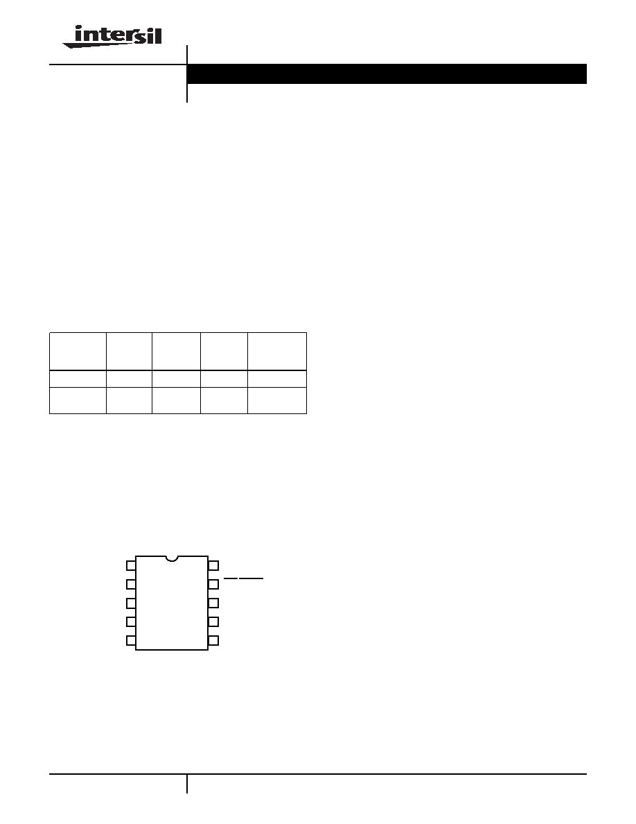
Pinout
ISL1221
(10 LD MSOP)
TOP VIEW
Features
· Real Time Clock/Calendar
- Tracks Time in Hours, Minutes, and Seconds
- Day of the Week, Day, Month, and Year
· Security and Event Functions
- Tamper detection with Time Stamp in Normal and
Battery Backed modes
- Event Detection During Battery Backed or Normal
Modes
- Selectable Event Input Sampling Rates Allows Low
Power Operation
- Selectable Glitch Filter on Event Input Monitor
· Separate F
OUT
pin with 15 Selectable Frequencies
· Single Alarm
- Settable to the Second, Minute, Hour, Day of the Week,
Day, or Month
- Single Event or Pulse Interrupt Mode
· Automatic Backup to Battery or Super Cap
· Power Failure Detection
· On-Chip Oscillator Compensation
· 2 Bytes Battery-Backed User SRAM
· I
2
C Interface
- 400kHz Data Transfer Rate
· 400nA Battery Supply Current
· Small Package
- 10 Ld MSOP
· Pb-Free Plus Anneal Available (RoHS Compliant)
Applications
· Utility Meters
· Set Top Box/Modem
· POS Equipment
· Network Routers, Hubs, Switches, Bridges
· Cellular Infrastructure Equipment
· Fixed Broadband Wireless Equipment
· Test Meters/Fixtures
· Vending Machine Management
· Security and Anti Tampering Applications
- Panel/Enclosure Status
- Warranty Reporting
- Time Stamping Applications
- Patrol/Security Check (Fire or Light Equipment)
- Automotive Applications
Ordering Information
PART
NUMBER
(Note)
PART
MARKING
V
DD
RANGE
TEMP
RANGE
(°C)
PACKAGE
(Pb-Free)
ISL1221IUZ
1221Z
2.7V to 5.5V -40 to +85 10 Ld MSOP
ISL1221IUZ-T 1221Z
2.7V to 5.5V -40 to +85 10 Ld MSOP
Tape and Reel
NOTE: Intersil Pb-free products employ special Pb-free material sets;
molding compounds/die attach materials and 100% matte tin plate
termination finish, which are RoHS compliant and compatible with both
SnPb and Pb-free soldering operations. Intersil Pb-free products are
MSL classified at Pb-free peak reflow temperatures that meet or exceed
the Pb-free requirements of IPC/JEDEC J STD-020.
1
2
3
4
10
9
8
7
5
6
X1
X2
V
BAT
GND
EVIN
V
DD
IRQ/EVDET
SCL
SDA
F
OUT
Data Sheet
June 22, 2006
2
FN6316.0
June 22, 2006
Block Diagram
I
2
C
INTERFACE
CONTROL
LOGIC
ALARM
FREQUENCY
OUT
RTC
DIVIDER
SDA
BUFFER
CRYSTAL
OSCILLATOR
POR
SWITCH
SCL
BUFFER
SDA
SCL
X1
X2
V
DD
V
BAT
IRQ/
EVDET
INTERNAL
SUPPLY
V
TRIP
Seconds
Minutes
Hours
Day of Week
Date
Month
Year
USER
SRAM
CONTROL
REGISTERS
EVIN
GND
F
OUT
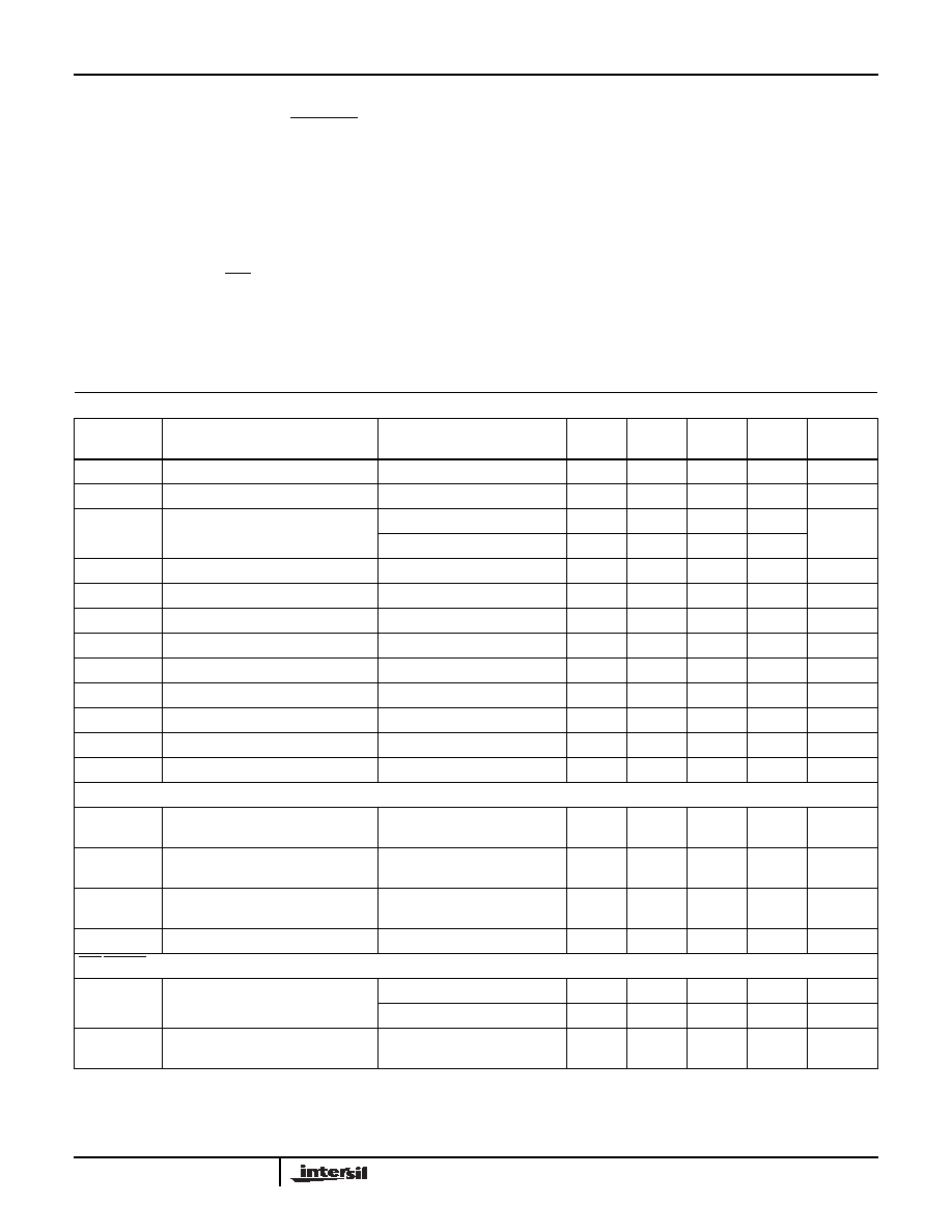
Pin Descriptions
PIN
NUMBER
SYMBOL
DESCRIPTION
1
X1
X1. The X1 pin is the input of an inverting amplifier and is intended to be connected to one pin of an external
32.768kHz quartz crystal. X1 can also be driven directly from a 32.768kHz source.
2
X2
X2. The X2 pin is the output of an inverting amplifier and is intended to be connected to one pin of an external
32.768kHz quartz crystal. X2 should be left open when X1 is driven from external source.
3
V
BAT
V
BAT.
This input provides a backup supply voltage to the device. V
BAT
supplies power to the device in the event that
the V
DD
supply fails. This pin should be tied to ground if not used.
4
GND
Ground.
5
EVIN
Event Input (EVIN). The EVIN is an input pin that is used to detect an externally monitored event. When a high signal
is present at the EVIN pin an "event" is detected.
6
F
OUT
Frequency Output F
OUT
, Frequency output pin, 15 selectable frequencies. Open drain output.
7
SDA
Serial Data (SDA). SDA is a bidirectional pin used to transfer serial data into and out of the device. It has an open
drain output and may be wire OR'ed with other open drain or open collector outputs.
8
SCL
Serial Clock (SCL). The SCL input is used to clock all serial data into and out of the device.Open drain output.
9
IRQ/EVDET Interrupt (IRQ)/Event Detect (EVDET) Output
.
Multi-functional pin that can be used as interrupt for Alarm and Event
Detect. Open Drain Output.
10
V
DD
V
DD.
Power supply.
ISL1221
3
FN6316.0
June 22, 2006
Absolute Maximum Ratings
Thermal Information
Voltage on V
DD
, V
BAT
, SCL, SDA, and IRQ/EVDET Pins
(respect to ground) . . . . . . . . . . . . . . . . . . . . . . . . . . -0.5V to 7.0V
Voltage on X1 and X2 Pins
(respect to ground) . . . . . . . . . . . .-0.5V to V
DD
+ 0.5 (V
DD
Mode)
-0.5V to V
BAT
+ 0.5 (V
BAT
Mode)
Maximum Junction Temperature (Plastic Package). . . . . . . . . 150°C
Storage Temperature . . . . . . . . . . . . . . . . . . . . . . . .-65°C to +150°C
Lead Temperature (Soldering, 10s) . . . . . . . . . . . . . . . . . . . . . 300°C
ESD Rating (Human Body Model) . . . . . . . . . . . . . . . . . . . . . . .>2kV
ESD Rating (Machine Model . . . . . . . . . . . . . . . . . . . . . . . . . .>175V
Output Current Sink (F
OUT
, IRQ . . . . . . . . . . . . . . . . . . . . . . . . 3mA
Thermal Resistance (Typical, Note 1)
JA
(°C/W)
10Ld MSOP Package. . . . . . . . . . . . . . . . . . . . . . . .
120
Moisture Sensitivity (see Technical Brief TB363). . . . . . . . . . Level 2
Recommended
Operating Conditions
Ambient Temperature . . . . . . . . . . . . . . . . . . . . . . . . . -40°C to 85°C
V
DD
Voltage. . . . . . . . . . . . . . . . . . . . . . . . . . . . . . . . . . 2.7V to 5.5V
V
BAT
Voltage . . . . . . . . . . . . . . . . . . . . . . . . . . . . . . . . . 1.8V to 5.5V
CAUTION: Stresses above those listed in "Absolute Maximum Ratings" may cause permanent damage to the device. This is a stress only rating and operation of the
device at these or any other conditions above those indicated in the operational sections of this specification is not implied.
NOTE:
1.
JA
is measured with the component mounted on a high effective thermal conductivity test board in free air. See Tech Brief TB379 for details.
DC Operating Characteristics RTC
Test Conditions: V
DD
= +2.7 to +5.5V, Temperature = -40°C to +85°C, unless otherwise stated.
SYMBOL
PARAMETER
CONDITIONS
MIN
TYP
(Note 5)
MAX
UNITS
NOTES
V
DD
Main Power Supply
2.7
5.5
V
V
BAT
Battery Supply Voltage
1.8
5.5
V
I
DD1
Supply Current
V
DD
= 5V
2
6
µA
2, 3
V
DD
= 3V
1.2
4
µA
I
DD2
Supply Current With I
2
C Active
V
DD
= 5V
40
120
µA
2, 3
I
DD3
Supply Current (Low Power Mode)
V
DD
= 5V, LPMODE = 1
1.4
5
µA
2, 8
I
BAT
Battery Supply Current
V
BAT
= 3V
400
950
nA
2
I
BATLKG
Battery Input Leakage
V
DD
= 5.5V, V
BAT
= 1.8V
100
nA
I
LI
Input Leakage Current on SCL
100
nA
I
LO
I/O Leakage Current on SDA
100
nA
V
TRIP
V
BAT
Mode Threshold
1.6
2.2
2.64
V
V
TRIPHYS
V
TRIP
Hysteresis
10
35
60
mV
V
BATHYS
V
BAT
Hysteresis
10
50
100
mV
EVIN
V
IL
-0.3
0.3 x
V
DD
V
V
IH
0.7 x
V
DD
V
DD
+
0.3
V
Hysteresis
0.05 x
V
DD
V
I
EVPU
EVIN Pullup Current
V
SUP
= 3V
1.5
µA
6
IRQ/EVDET and F
OUT
V
OL
Output Low Voltage
V
DD
= 5V, I
OL
= 3mA
0.4
V
V
DD
= 2.7V, I
OL
= 1mA
0.4
V
I
LO
Output Leakage Current
V
DD
= 5.5V
V
OUT
= 5.5V
100
400
nA
ISL1221
4
FN6316.0
June 22, 2006
Power-Down Timing
Test Conditions: V
DD
= +2.7 to +5.5V, Temperature = -40°C to +85°C, unless otherwise stated.
SYMBOL
PARAMETER
CONDITIONS
MIN
TYP
(Note 5)
MAX
UNITS
NOTES
V
DD SR-
V
DD
Negative Slew rate
10
V/ms
4
I
2
C Interface Specifications
Test Conditions: V
DD
= +2.7 to +5.5V, Temperature = -40°C to +85°C, unless otherwise specified.
SYMBOL
PARAMETER
TEST CONDITIONS
MIN
TYP
(Note 5)
MAX
UNITS
NOTES
V
IL
SDA and SCL Input Buffer LOW
Voltage
-0.3
0.3 x
V
DD
V
V
IH
SDA and SCL Input Buffer HIGH
Voltage
0.7 x
V
DD
V
DD
+
0.3
V
Hysteresis
SDA and SCL Input Buffer
Hysteresis
0.05 x
V
DD
V
V
OL
SDA Output Buffer LOW Voltage,
Sinking 3mA
V
DD
= 5V, I
OL
= 3mA
0.4
V
Cpin
SDA and SCL Pin Capacitance
T
A
= 25°C, f = 1MHz, V
DD
= 5V,
V
IN
= 0V, V
OUT
= 0V
10
pF
f
SCL
SCL Frequency
400
kHz
t
IN
Pulse Width Suppression Time at
SDA and SCL Inputs
Any pulse narrower than the max spec
is suppressed.
50
ns
t
AA
SCL falLing Edge to SDA Output
Data Valid
SCL falling edge crossing 30% of V
DD
,
until SDA exits the 30% to 70% of V
DD
window.
900
ns
t
BUF
Time the Bus Must be Free Before
the Start of a New Transmission
SDA crossing 70% of V
DD
during a
STOP condition, to SDA crossing 70%
of V
DD
during the following START
condition.
1300
ns
t
LOW
Clock LOW Time
Measured at the 30% of V
DD
crossing.
1300
ns
t
HIGH
Clock HIGH Time
Measured at the 70% of V
DD
crossing.
600
ns
t
SU:STA
START Condition Setup Time
SCL rising edge to SDA falling edge.
Both crossing 70% of V
DD
.
600
ns
t
HD:STA
START Condition Hold Time
From SDA falling edge crossing 30%
of V
DD
to SCL falling edge crossing
70% of V
DD
.
600
ns
t
SU:DAT
Input Data Setup Time
From SDA exiting the 30% to 70% of
V
DD
window, to SCL rising edge
crossing 30% of V
DD.
100
ns
t
HD:DAT
Input Data Hold Time
From SCL falling edge crossing 30% of
V
DD
to SDA entering the 30% to 70%
of V
DD
window.
0
900
ns
t
SU:STO
STOP Condition Setup Time
From SCL rising edge crossing 70% of
V
DD
, to SDA rising edge crossing 30%
of V
DD
.
600
ns
t
HD:STO
STOP Condition Hold Time
From SDA rising edge to SCL falling
edge. Both crossing 70% of V
DD
.
600
ns
t
DH
Output Data Hold Time
From SCL falling edge crossing 30% of
V
DD
, until SDA enters the 30% to 70%
of V
DD
window.
0
ns
t
R
SDA and SCL Rise Time
From 30% to 70% of V
DD.
20 +
0.1 x Cb
300
ns
7
ISL1221
5
FN6316.0
June 22, 2006
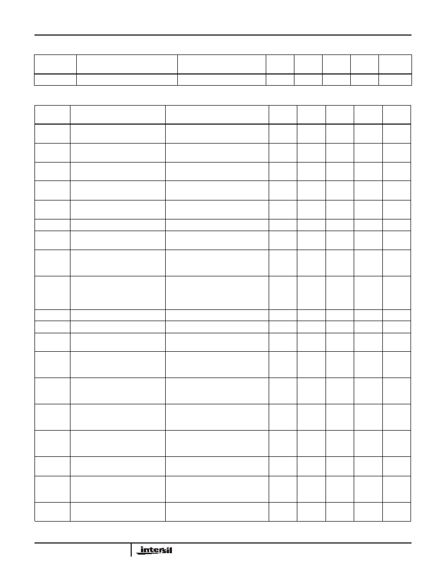
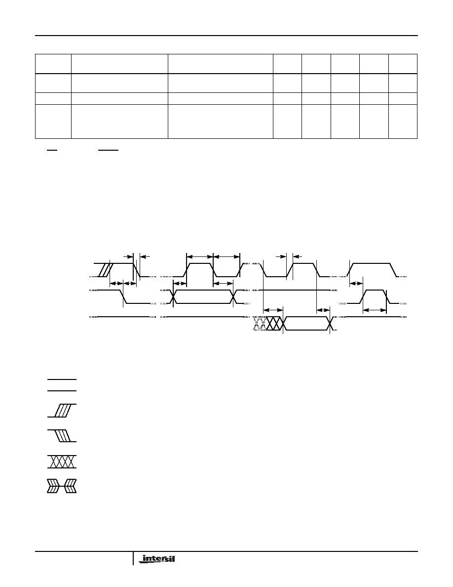
SDA vs. SCL Timing
Symbol Table
t
F
SDA and SCL Fall Time
From 70% to 30% of V
DD.
20 +
0.1 x Cb
300
ns
7
Cb
Capacitive Loading of SDA or SCL Total on-chip and off-chip
10
400
pF
7
Rpu
SDA and SCL Bus Pull-up Resistor
Off-chip
Maximum is determined by t
R
and t
F
.
For Cb = 400pF, max is about
2~2.5k
. For Cb = 40pF, max is about
15~20k
1
k
7
NOTES:
2. IRQ and F
OUT
and EVDET Inactive.
3. LPMODE = 0 (default).
4. In order to ensure proper timekeeping, the V
DD SR-
specification must be followed.
5. Typical values are for T = 25°C and 3.3V supply voltage.
6. V
SUP
= V
DD
if in V
DD
Mode, V
SUP
= V
BAT
if in V
BAT
Mode.
7. These are I
2
C specific parameters and are not directly tested, however they are used during device testing to validate device specification.
8. A write to register 08h should only be done if V
DD
> V
BAT
, otherwise the device will be unable to communicate using I
2
C.
I
2
C Interface Specifications
Test Conditions: V
DD
= +2.7 to +5.5V, Temperature = -40°C to +85°C, unless otherwise specified.
SYMBOL
PARAMETER
TEST CONDITIONS
MIN
TYP
(Note 5)
MAX
UNITS
NOTES
t
SU:STO
t
DH
t
HIGH
t
SU:STA
t
HD:STA
t
HD:DAT
t
SU:DAT
SCL
SDA
(INPUT TIMING)
SDA
(OUTPUT TIMING)
t
F
t
LOW
t
BUF
t
AA
t
R
WAVEFORM
INPUTS
OUTPUTS
Must be steady
Will be steady
May change
from LOW
to HIGH
Will change
from LOW
to HIGH
May change
from HIGH
to LOW
Will change
from HIGH
to LOW
Don't Care:
Changes Allowed
Changing:
State Not Known
N/A
Center Line is
High Impedance
ISL1221