
HI-15530
Manchester Encoder / Decoder
PIN CONFIGURATION
(Top View)
24 VDD
23 ENCODER CLK
22 SEND CLK IN
21 SEND DATA
20 SYNC SELECT
19 ENCODER ENABLE
18 SERIAL DATA IN
17
16
15
14
6 OUT
13 MASTER RESET
BIPOLAR ONE OUT
OUTPUT INHIBIT
BIPOLAR ZERO OUT
˜
VALID WORD 1
ENCODER SHIFT CLK
2
TAKE DATA
3
SERIAL DATA OUT
4
DECODER CLK
5
BIPOLAR ZERO IN 6
BIPOLAR ONE IN 7
UNIPOLAR DATA IN 8
DECODER SHIFT CLK
9
COMMAND /
SYNC 10
DECODER RESET 11
GND 12
DATA
HI-15530PSI
24 Pin SOIC package
GENERAL DESCRIPTION
The HI-15530 is a high performance CMOS integrated
circuit designed to meet the requirements of Mil-Std-1553
and similar Manchester II encoded, time division
multiplexed serial data protocols. The HI-15530 contains
both an Encoder and Decoder, which operate
independently.
The device generates Mil-Std-1553 sync pulses, parity bits
as well as the Manchester II encoding of the data bits. The
decoder recognizes and identifies sync pulses, decodes
data bits, and performs parity checking.
The HI-15530 supports the 1Mbit/s data rate of Mil-Std-
1553 over the full temperature and voltage range.
For applications requiring small footprints and low cost, the
HI-15530 is available in a 24-pin plastic SOIC package.
Ceramic DIP and LCC packages are also available to
achieve the highest level of reliability and to provide drop-in
replacement for obsolete parts from other manufacturers.
APPLICATIONS
!
!
!
Mil-Std-1553 Interfaces
Smart Munitions
Stores management
!
!
!
ARINC 708A Interfaces
Sensor interfaces
Instrumentation
FEATURES
!
!
!
!
Mil-Std-1553 compatible
Interfaces to HI-1567 Transceiver
1.25 Mbit/s Data Rate
Clock recovery
!
!
!
!
Small footprint 24-pin plastic SOIC package
option
Direct replacement for:
Harris HD15530
GEC Plessey Semiconductors MAS15530
Aeroflex ACT15530
Manchester II Encode and Decode
Sync identification and Lock-in
July 2001
HOLT INTEGRATED CIRCUITS
(DS15530 Rev. A)
07/01

SIGNAL
FUNCTION
DESCRIPTION
VALID WORD
OUTPUT
A high output signals the receipt of a valid word
ENCODER SHIFT CLOCK
OUTPUT
Shifts data into the encoder on a low to high transition
TAKE DATA
OUTPUT
Output is high during receipt of data after identification of a Sync
Pulse and two valid Manchester data bits.
SERIAL DATA OUT
OUTPUT
Received Data output in NRZ format
DECODER CLOCK
INPUT
12x the data rate. Clock for the transition finder and synchronizer,
which generates the internal clock for the remainder of the decoder
BIPOLAR ZERO IN
INPUT
A high input indicates the 1553 bus is in its negative state.
This pin must be held high when the Unipolar input is used
BIPOLAR ONE IN
INPUT
A high input indicates the 1553 bus is in the positive state.
This pin must be held low when the Unipolar input is used
UNIPOLAR DATA IN
INPUT
Input for unipolar data to the transition finder. Must be held low when
not in use
DECODER SHIFT CLOCK
OUTPUT
Provides the DECODER CLOCK divided by 12, synchronized by the
recovered serial data
COMMAND /
SYNC
OUTPUT
A high on this pin occurs during the output of decoded data which
was preceded by a Command (or Status) synchronizing character. A
low output indicates a Data synchronizing character
DECODER RESET
INPUT
A high applied to this pin during a DECODER SHIFT CLOCK rising
edge resets the bit counter
GND
POWER
0V supply
MASTER RESET
INPUT
A high on this pin clears 2:1 counters in both Encoder and Decoder,
and resets the divide-by-6 circuit
6 OUT
OUTPUT
Provides ENCODER CLOCK divided by 6
OUTPUT
An active low output intended to drive the zero or negative sense of a
MIL-STD-1553 Line Driver
INPUT
A low inhibits the
and
by
forcing them to inactive high states
OUTPUT
An active low output intended to drive the one or positive sense on a
MIL-STD-1553 Line Driver
SERIAL DATA IN
INPUT
Receiver serial data at the rate of the ENCODER SHIFT CLOCK
ENCODER ENABLE
INPUT
A high on this pin initiates the encode cycle. (Subject to the
preceeding cycle being complete)
SYNC SELECT
INPUT
Actuates a Command Sync for an input high and a Data Sync for a
low
SEND DATA
OUTPUT
An active high output which enables the external source of serial
Data
SEND CLOCK IN
INPUT
Clock input at 2 times the Data rate, usualy driven by 6 OUT
ENCODER CLOCK
INPUT
Input to the divide by 6 circuit. Normal frequency is Data rate x12
VDD
POWER
5V +/- 10%
DATA
BIPOLAR ZERO OUT
OUTPUT INHIBIT
BIPOLAR ZERO OUT
BIPOLAR ONE OUT
BIPOLAR ONE OUT
˜
˜
PIN DESCRIPTIONS
HOLT INTEGRATED CIRCUITS
2
HI-15530

ENCODER OPERATION
HI-15530
HOLT INTEGRATED CIRCUITS
3
The encoder requires a single clock with a frequency of
twice the desired rate applied at the SEND CLOCK input.
An auxiliary divide by six counter is provided on chip which
can be utilized to produce the SEND CLOCK by dividing
the ENCODER CLOCK.
The Encoder's cycle begins when ENCODER ENABLE is
high during a falling edge of ENCODER SHIFT CLOCK (1).
This cycle lasts for one word length or twenty ENCODER
SHIFT CLOCK periods. At the next low-to-high transition of
the ENCODER SHIFT CLOCK, a high at SYNC SELECT
input actuates a command sync or a low will produce a
data sync for that word (2). When the Encoder is ready to
accept data, the SEND DATA output will go high and
remain high for sixteen ENCODER SHIFT CLOCK periods
(3). During these sixteen periods the data should be
clocked into the SERIAL DATA input with every low-to-high
transition of the ENCODER SHIFT CLOCK (3) - (4). After
the sync and the Manchester II coded data are transmitted
through the
and
outputs,
the Encoder adds on an additional bit which is the parity for
that word (5). If ENCODER ENABLE is held high continu-
ously, consecutive words will be encoded without an
interframe gap. ENCODER ENABLE must go low by time
(5) as shown to prevent a consecutive word from being
encoded. At any time a low on the
input
will force both bipolar outputs to a high state but will not
affect the Encoder in any other way.
BIPOLAR ONE
BIPOLAR ZERO
OUTPUT INHIBIT
0
1
2
3
4
5
6
7
15
16
17
18
19
15
14
13
12
11
3
2
1
0
P
3
2
1
0
P
15
14
13
12
11
SYNC
SYNC
SYNC
15
14
13
12
11
3
2
1
0
10
SYNC
VALID
(1) (2)
(3)
(4) (5)
DON'T CARE
DON'T CARE
SYNC SELECT
ENCODER
ENABLE
ENCODER
SHIFT CLK
SEND CLK
TIMING
SEND DATA
SERIAL
DATA IN
BIPOLAR
ONE OUT
BIPLOAR
ZERO OUT
Bit
Counter
Character
Former
˜
6
˜2
˜
6
MASTER RESET
SEND CLK IN
˜
6 OUT
ENCODER CLK
SEND
DATA
ENCODER
SHIFT
CLK
SERIAL
DATA
IN
ENCODER
ENABLE
SYNC
SELECT
OUTPUT
INHIBIT
BIPOLAR
ONE OUT
BIPOLAR
ZERO OUT
Bit
Counter
Character
Former
˜
6
˜2
˜
6
MASTER RESET
SEND CLK IN
˜
6 OUT
ENCODER CLK
SEND
DATA
ENCODER
SHIFT
CLK
SERIAL
DATA
IN
ENCODER
ENABLE
SYNC
SELECT
OUTPUT
INHIBIT
BIPOLAR
ONE OUT
BIPOLAR
ZERO OUT
To abort the Encoder transmission a positive pulse must be
applied at MASTER RESET. Anytime after or during this
pulse, a low to high transition on SEND CLOCK clears the
internal counters and initializes the Encoder for a new
word.

The Decoder requires a single clock with a frequency of 12
times the desired data rate applied at the DECODER
CLOCK input. The Manchester II coded data can be
presented to the Decoder in one of two ways. The
BIPOLAR ONE and BIPOLAR ZERO inputs will accept
data from a comparator sensed transformer coupled bus as
specified in MIL-STD-1553. The UNIPOLAR DATA input
can only accept non-inverted Manchester II coded data
(e.g. from
of an Encoder). The
Decoder is free running and continuously monitors its data
input lines for a valid sync character and two valid
Manchester data bits to start an output cycle. When a valid
sync is recognized (1), the type of sync is indicated on
COMMAND/
SYNC output. If the sync character was
a command sync, this output will go high (2) and remain
high for sixteen DECODER SHIFT CLOCK periods (3),
otherwise it will remain low. The TAKE DATA output will go
high and remain high (2) - (3) while the Decoder is
transmitting the decoded data through SERIAL DATA OUT.
The decoded data available at SERIAL DATA OUT is in a
NRZ format. The DECODER SHIFT CLOCK is provided so
that the decoded bits can be shifted into an external register
on every low-to-high transition of this clock (2) - (3). After all
sixteen decoded bits have been transmitted (3) the data is
checked for odd parity. A high on VALID WORD output (4)
indicates a successful reception of a word without any
Manchester or parity errors. At this time the Decoder is
BIPOLAR ZERO OUT
DATA
HI-15530
HOLT INTEGRATED CIRCUITS
4
DECODER OPERATION
0
1
2
3
4
5
6
7
16
17
18
19
15
14
13
12
11
2
1
0
P
2
1
0
P
15
14
13
12
11
SYNC
SYNC
SYNC
15
14
13
12
3
2
1
0
SYNC
(1)(2)
(3)
(4)
May be high from previous reception
VALID WORD
DECODER
SHIFT CLK
TIMING
TAKE DATA
SERIAL
DATA OUT
BIPOLAR
ONE IN
BIPLOAR
ZERO IN
8
COMMAND /
SYNC
DATA
10
10
4
UNDEFINED
TAKE DATA
UNIPOLAR
DATA IN
BIPOLAR
ONE IN
BIPOLAR
ZERO IN
MASTER
RESET
DECODER
CLK
DECODER
RESET
COMMAND/
SYNC
DATA
SERIAL DATA
OUT
VALID
WORD
DECODER
SHIFT CLK
TRANSITION
FINDER
CHARACTER
IDENTIFIER
SYNCHRONIZER
BIT
COUNTER
BIT
RATE
CLK
PARITY
CHECK
looking for a new sync character to start another output
sequence. VALID WORD will go low approximately 20
DECODER SHIFT CLOCK periods after it goes high if not
reset low sooner by a valid sync and two valid Manchester
bits as shown (1). At any time in the above sequence, a
high input on DECODER RESET during a low-to-high
transition of DECODER SHIFT CLOCK will abort
transmission and initialize the Decoder to start looking for a
new sync character.

HI-15530
HOLT INTEGRATED CIRCUITS
5
ENCODER
SHIFT CLK
SERIAL DATA IN
SEND CLK
SEND CLK
ENCODER ENABLE
SEND DATA
SEND CLK
ENCODER
SHIFT CLK
SYNC SELECT
ENCODER
SHIFT CLK
BIPOLAR ONE OUT
BIPOLAR ZERO OUT
or
VALID
t
E1
t
E2
t
E1
t
E4
t
E5
t
E6
t
E7
t
E8
t
E9
VALID
COMMAND /
SYNC
DATA
SERIAL DATA OUT
t
D6
t
D7
TAKE DATA
t
D8
DECODER SHIFT CLK
DECODER SHIFT CLK
DATA BIT
COMMAND /
SYNC
DATA
t
D9
t
D10
TAKE DATA
DECODER SHIFT CLK
t
D11
VALID WORD
t
DRH
t
DRS
DECODER SHIFT CLK
t
DR
DECODER RESET
t
E3
VALID

HI-15530
HOLT INTEGRATED CIRCUITS
6
BIPOLAR ZERO IN
t
D2
BIPOLAR ONE IN
BIT PERIOD
BIT PERIOD
BIT PERIOD
t
D1
t
D1
t
D3
t
D3
BIPOLAR ZERO IN
t
D2
BIPOLAR ONE IN
t
D1
t
D1
t
D3
t
D3
t
D2
BIPOLAR ZERO IN
BIPOLAR ONE IN
t
D1
t
D3
t
D3
t
D1
t
D4
t
D3
t
D1
t
D3
t
D5
t
D5
t
D4
t
D1
t
D3
UNIPOLAR IN
UNIPOLAR IN
UNIPOLAR IN
t
D2
t
D4
t
D4
t
D2
t
D2
t
D2
t
D5
t
D4
t
D5
t
D2
COMMAND SYNC
DATA SYNC
ZERO
ONE
ONE
ZERO
ONE
ONE
COMMAND SYNC
DATA SYNC
0
1
2
3
4
5
6
7
8
9 10
12
11
13 14 15 16 17 18 19
Bit Period
Command Word
Data Word
Status Word
R/T
SUBADDRESS
/ MODE
DATA WORD
COUNT
P
P
P
DATA WORD
TERMINAL ADDRESS
ME
CODE FOR FAILURE MODES
TERMINAL ADDRESS
SYNC
SYNC
SYNC
SYNC
SYNC
SYNC
TF
HI-15530
HOLT INTEGRATED CIRCUITS
7
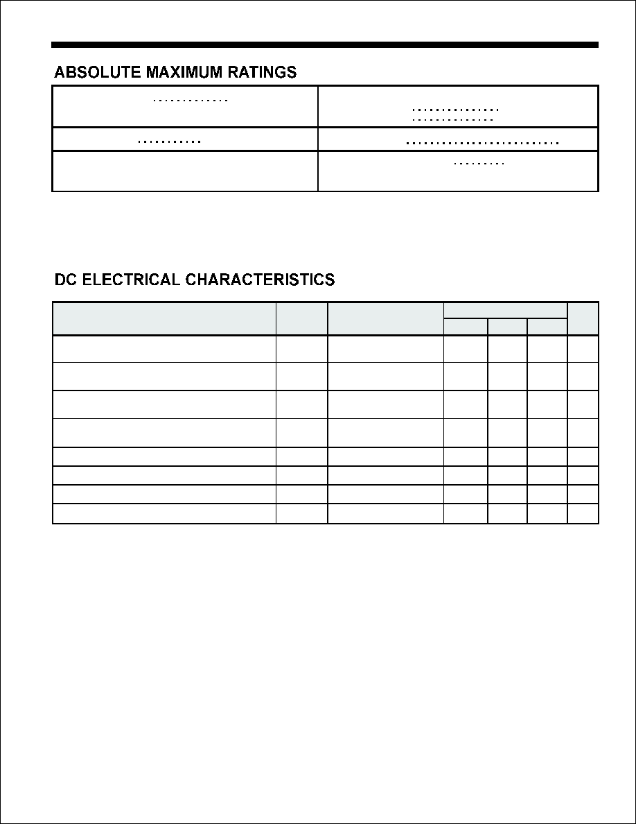
LIMITS
PARAMETER
CONDITIONS
UNIT
SYMBOL
Input Voltage
Input Voltage HI
V
70% V
V
Input Voltage LO
VIL
30% V
V
Clock Input Voltage
Input Voltage HI
V
V
-0.5
V
Input Voltage LO
V
0.5V
V
Input Leakage Current
Input Sink
I
1.0
Input Source
I
-1.0
MIN
TYP
MAX
IH
DD
DD
IHC
DD
ILC
IH
IL
µA
µA
Output Voltage
Logic "1" Output Voltage
V
I
=-3mA
2.4
V
Logic "0" Output Voltage
V
I
=1.8mA
0.4
V
Standby Supply Current
I
V =V
, Outputs Open
2.0
mA
Operating Supply Current
I
f=1MHz, Outputs Open
10.0
mA
Input Capacitance
C
7.0
pF
Output Capacitance
C
10.0
pF
OH
OH
OL
OL
DDSB
IN
DD
DD
IN
OUT
V
= 5V ±10%, GND = 0V, TA = Operating Temperature Range (unless otherwise specified).
DD
Power Dissipation at 25C
Plastic SOIC
1.5 W, derate10mW/ C
Ceramic DIP
1.0 W, derate 7mW/
DC Current Drain per pin
±10mA
∞
∞C
Storage Temperature Range:
-65∞C to +150∞C
Supply Voltage V
-0.3V to +7V
V
DD
oltage at any pin
-0.3V to Vcc +0.3V
Operating Temperature Range:
(Industrial)
-40∞C to +85∞C
(Military)
-55∞C to +125∞C
NOTE: Stresses above those listed under "Absolute Maximum Ratings" may cause permanent damage to the device. These are stress ratings
only. Functional operation of the device at these or any other conditions above those indicated in the operational sections of the specifications is not
implied. Exposure to absolute maximum rating conditions for extended periods may affect device reliability.

HOLT INTEGRATED CIRCUITS
8
HI-15530
LIMITS
PARAMETER
SYMBOL
UNITS
MIN
TYP
MAX
Encoder Timing
Decoder Timing
Encoder Clock Frequency
fEC
0
15
MHz
Send Clock Frequency
fESC
0
2.5
MHz
Encoder Clock Rise Time
tECR
8
ns
Encoder Clock Fall Time
tECF
8
ns
Encoder Data Rate
fED
0
1.25
MHz
Master Reset Pulse Width
tMR
150
ns
Shift Clock Delay
tE1
125
ns
Serial Data Setup Time
tE2
75
ns
Serial Data Hold Time
tE3
75
ns
Enable Setup Time
tE4
90
ns
Enable Pulse Width
tE5
80
ns
Sync Setup Time
tE6
55
ns
Sync Pulse Width
tE7
150
ns
Send Data Delay
tE8
0
50
ns
Bipolar Output Delay
tE9
130
ns
Enable Hold Time
tE10
10
ns
Sync Hold Time
tE11
95
ns
Decoder Clock Frequency
fDC
0
15
MHz
Decoder Clock Rise Time
tDCR
8
ns
Decoder Clock Fall Time
tDCF
8
ns
Decoder Data Rate
fDD
0
1.25
MHz
Decoder Reset Pulse Width
tDR
150
ns
Decoder Reset Setup Time
tDRS
75
ns
Decoder Reset Hold Time
Master Reset Pulse Width
tMR
150
ns
Bipolar Data Pulse Width
tD1
tDC+10
ns
Sync Transition Span
tD2
18tDC
ns
One-Zero Overlap
tD3
tDC-10
ns
Short Data Transition Span
tD4
6tDC
ns
Long Data Transition Span
tD5
12tDC
ns
Sync Delay (On)
tD6
-20
110
ns
Take Data Delay (On)
tD7
0
110
ns
Serial Data Out Delay
tD8
80
ns
Sync Delay (Off)
tD9
0
110
ns
Take Data Delay (Off)
tD10
0
110
ns
Valid Word Delay
tD11
0
110
ns
tDRH
10
ns
VDD = 5V
, GND = 0V, TA = Operating Temperature Range, CL=50pF
±10%

HOLT INTEGRATED CIRCUITS
9
HI-15530
PART
NUMBER
PACKAGE
DESCRIPTION
TEMPERATURE
RANGE
FLOW BURN
IN
LEAD
FINISH
HI-15530CDI
24 PIN CERAMIC SIDE BRAZED DIP
-40∞C TO +85∞C
I
NO
GOLD
HI-15530CDT
24 PIN CERAMIC SIDE BRAZED DIP
-55∞C TO +125∞C
T
NO
GOLD
HI-15530CDM
24 PIN CERAMIC SIDE BRAZED DIP
-55∞C TO +125∞C
M
YES
SOLDER
HI-15530PSI
24 PIN PLASTIC SOIC
-40∞C TO +85∞C
I
NO
SOLDER
HI-15530PST
24 PIN PLASTIC SOIC
-55∞C TO +125∞C
T
NO
SOLDER
HI-15530CLI
24 PIN CERAMIC LEADLESS CHIP CARRIER -40∞C TO +85∞C
I
NO
GOLD
HI-15530CLT
24 PIN CERAMIC LEADLESS CHIP CARRIER -55∞C TO +125∞C
T
NO
GOLD
HI-15530CLM
24 PIN CERAMIC LEADLESS CHIP CARRIER -55∞C TO +125∞C
M
YES
SOLDER
VALID WORD 1
ENCODER SHIFT CLK
2
TAKE DATA
3
SERIAL DATA OUT
4
DECODER CLK
5
BIPOLAR ZERO IN 6
BIPOLAR ONE IN 7
UNIPOLAR DATA IN 8
DECODER SHIFT CLK
9
COMMAND /
SYNC 10
DECODER RESET 11
GND 12
DATA
24 VDD
23 ENCODER CLK
22 SEND CLK IN
21 SEND DATA
20 SYNC SELECT
19 ENCODER ENABLE
18 SERIAL DATA IN
17
16
15
14
6 OUT
13 MASTER RESET
BIPOLAR ONE OUT
OUTPUT INHIBIT
BIPOLAR ZERO OUT
˜
28 - Pin Ceramic LCC
24 - Pin Ceramic Side-Brazed DIP
4
3
2
1 28 27 26
12 13 14 15 16 17 18
5
6
7
8
9
10
11
25
24
23
22
21
20
19
SEND DATA
N/C
N/C
SYNC SELECT
ENCODER ENABLE
SERIAL DATA IN
BIPOLAR ONE OUT
DECODER CLK
N/C
N/C
BIPOLAR ZERO IN
BIPOLAR ONE IN
UNIPOLAR DATA IN
DECODER SHIFT CLOCK
HI-15530CLI
HI-15530CLT
HI-15530CLM
HI-15530CDI
HI-15530CDT
HI-15530CDM

Package Type:
1.220 MAX
(30.988 MAX)
.225 MAX
(5.715 MAX)
.100 BSC
(2.540 BSC)
.018 TYP
(.457 TYP)
.050 TYP
(1.270 TYP)
.085
±
.009
(2.159
±
.229)
.125 MIN
(3.175 MIN)
.610
±
.010
(15.494
±
.254)
.600
±
.010
(15.240
±
.254)
.595
±
.010
(15.113
±
.254)
.010
+
.002
/-
.001
(.254
+
.051
/-
.025)
24-PIN CERAMIC SIDE-BRAZED DIP
24C
HOLT INTEGRATED CIRCUITS
10
HI-15530
.307 ± .016
(7.80 ± .40)
.209 ± .012
(5.30 ± .30)
0∞ to 8∞
.005 ± .001
(.13 ± .08)
TYP
TYP
SEE DETAIL A
Package Type:
.323 ± .012
(8.20 ± .30)
.026
(.65)
.030 ± .008
(.75 ± .20)
.095 ± .005
(2.413 ± .127)
TYP
.012
(.30)
TYP
SEE DETAIL A
DETAIL A
Package Type:
24-PIN PLASTIC SSOP
24HS
.006
(.15)
TYP

HOLT INTEGRATED CIRCUITS
11
HI-15530
Package Type:
.451
±
.009
(11.455
±
.229)
SQ.
.080
±
.020
(2.032
±
.508)
.040 x 45∞ 3PLS
(1.016 x 45∞ 3PLS)
.050
±
.005
(1.270
±
.127)
.025
±
.003
(.635
±
.076)
.050 BSC
(1.270 BSC)
.008R ± .006
(.203R
±
.152)
.020 INDEX
(.508 INDEX)
PIN 1
28S
28-PIN CERAMIC LEADLESS CHIP CARRIER
PIN 1