HI-8050/51, HI-8150/51
CMOS HIGH VOLTAGE DISPLAY DRIVER
GENERAL DESCRIPTION
The HI-8050, HI-8051, HI-8150 and HI-8151 are CMOS
integrated circuits designed for high voltage LCD display
drive applications. The HI-8050 & HI-8051 have TTL logic
inputs whereas the HI-8150 & HI-8151 have CMOS logic
inputs. They drive up to 38 segments at voltages between
+5 and -30 volts. The optional negative converter on the
HI-8050 & HI-8150 can be used to generate the negative
display drive voltage.
All products have test inputs to
facilitate opens and shorts testing as well as automatic
blanking of the display if the +5V power is lost.
The HI-8050 and HI-8150 are designed to replace the
HI-8010 and HI-8020 devices in all 5 volt applications. They
offer significantly enhanced ESD protection along with a
considerably faster serial input data rate.
The data is serially clocked into the device on the negative
edge of the clock and latched in parallel to the segment
outputs on the high to low transition of the load input. Serial
output data changes on the positive edge of the clock
allowing the cascading ofmultiple drivers for larger displays.
The device layout supports all previous pinouts of the
HI-8010/HI-8020 products. In addition, new technology and
features afford new packaging options. Consult your Holt
Sales Representative to explore the possibilities.
!
!
Dichroic Liquid Crystal Displays
Standard Liquid Crystal Displays
!
5 Volt Serial Data to Parallel High Voltage
APPLICATIONS
!
!
!
!
!
!
!
!
!
4 MHz serial input data rate
38 segment outputs
Cascadable
5 Volt inputs translated to 35 Volts
Test pins allow hardware all "ON", all "OFF" or
alternating
Monitors 5 volt supply and forces all
segments to "OFF" condition if lost
Negative voltage converter available on-chip
CMOS low power
Military processing available
FEATURES
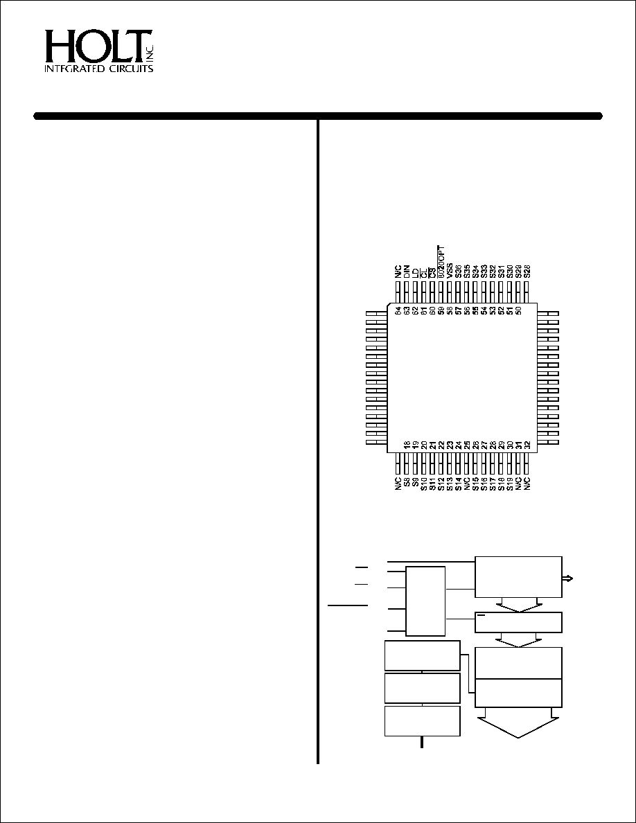
PAD CONFIGURATION
(Top View)
FUNCTIONAL BLOCK DIAGRAM
O s c i l l a t o r
D i v i d e r
V o l t a g e
T r a n s l a t o r
H i g h V o l t a g e
B u f f e r
3 8 S t a g e
S h i f t R e g i s t e r
3 8 B i t L a t c h
V o l t a g e
T r a n s l a t o r s
H i g h V o l t a g e
D r i v e r s
Þ
BPOUT
38 SEGMENTS
DIN
LD
BPIN
BPOSC
Þ
Þ
Þ
Þ
Þ
Þ
CL
CS
8020OPT
Þ
DATA IN
CLK
LE
DOUT38
DOUT32
DOUT30
CONTROL
LOGIC
January 2001
BPIN
BPOSC
VDD
N/C
CONVOSC
CONVOUT
VEE
S37
S38
S1
S2
S3
S4
S5
S6
S7
S27
S26
S25
S24
S23
S22
S21
S20
DOUT38
DOUT32
DOUT30
T2
T1
N/C
BPOUT
N/C
HI-8050PQI
HI-8150PQI
HI-8050PQT
&
HI-8150PQT
2
3
4
5
6
7
8
9
10
11
12
13
14
15
16
48
47
46
45
44
43
42
41
40
39
38
37
36
35
34
(See page 3-32A for HI-8051 & HI-8151 pin configurations)
HOLT INTEGRATED CIRCUITS
1
(DS8050 Rev. C)
01/01

HI-8050/51, HI-8150/51
PIN DESCRIPTION TABLE
VSS
POWER
0 Volts
LOGIC INPUT Open or high logic level selects the HI-8010/HI-8110
/
logic. A low
selects the HI-8020/HI-8120 Logic (HI-8050 & HI-8150 only)
LOGIC INPUT Chip select - Active low
LOGIC INPUT Serial data input clock - Active low
LD
LOGIC INPUT Latches data in shift register to the segment outputs - Active high
DIN
LOGIC INPUT Serial input data to the shift register
BPIN
INPUT
Backplane frequency input. Either driven from an external source or connected
to BPOSC and an external resistor and capacitor.
BPOSC
OUTPUT
Internal oscillator pin. Connected to BPIN and an external resistor and capacitor
VDD
POWER
+5V ±5%, Positive voltage of the backplane and segments
CONVOSC
INPUT
Used in conjunction with CONVOUT to generate the negative VEE voltage
on-chip (HI-8050 & HI-8150 only).
CONVOUT
OUTPUT
Used in conjunction with CONVOSC to generate the negative VEE voltage
on-chip (HI-8050 & HI-8150 only).
VEE
POWER
Negative voltage of the backplane and segments - between VSS and VDD- 35V
S1 to S38
OUTPUT
Segment outputs to LCD display
BPOUT
OUTPUT
Backplane output to LCD display (See Figure 3 for cascading drivers)
T1
LOGIC INPUT Used in conjunction with T2 to control display mode. Normal mode is logic low.
T2
LOGIC INPUT Used in conjunction with T1 to control display mode. Normal mode is logic low.
DOUT30
OUTPUT
Logic output from the 30th bit of the shift register. Use for pattern
verification or as the DIN of the next cascaded driver (HI-8050 & HI-8150 only).
DOUT32
OUTPUT
DOUT38
OUTPUT
SIGNAL
FUNCTION
DESCRIPTION
8020OPT
CL CS
CS
CL
Logic output from the 32nd bit of the shift register. Use for pattern
verification or as the DIN of the next cascaded driver (HI-8050 & HI-8150 only).
Logic output from the 38th bit of the shift register. Use for pattern
verification or as the DIN of the next cascaded driver.
HOLT INTEGRATED CIRCUITS
2

HI-8050/51, HI-8150/51
FUNCTIONAL DESCRIPTION
INPUT LOGIC
BPOSC and BPIN
The data is clocked into a serial shift register from the DIN in-
put on the negative edge of
while
is held low. LD is
normally held low and pulsed high only when data from the
shift register is parallel latched to the segment outputs.
must be low when LD is pulsed. The latches are transparent
while LD is high. A logic "1" in the shift register causes the
corresponding segment output to be out of phase with the
BP output. All four logic inputs are TTL compatible on the
HI-8050/51and CMOS compatible on the HI-8150/51.
The user has the option of creating the backplane frequency
internally or providing a signal from an external source. For
an internal oscillator, BPIN and BPOSC are connected to-
gether and the appropriate R & C combination is applied as
shown in Figure 1. The resulting backplane frequency is ap-
proximately:
f =
1
.
(R = 220K , C = 220pF, f
100HZ)
The value of the resistor must be greater than 30K .
Alternatively, BPOSC is left open and an external backplane
signal of the desired frequency is applied to the BPIN input.
CL
CS
CS
BP
BP
ª
VEE & NEGATIVE VOLTAGE CONVERTER
VEE can be connected to a negative power supply. Alterna-
tively, the HI-8050 & HI-8150 have the option of generating
the VEE voltage with a built-in -25 volt negative voltage con-
verter (See Figure 2). When not used, the open CONVOSC
pin is detected and all power consuming circuitry is dis-
abled. The converter will survive a short between two seg-
ments and stillmaintain a VEE voltage of -20V.
DOUT
The DOUT30, DOUT32, and DOUT38 pins are available for
cascading devices to drive more segments (See Figure 3) and
for verifying the integrity of the shift register data. The outputs
can drive 2 TTL loads. They change on the positive edge of
.
CL
AUTOMATIC SEGMENTS OFF
TEST INPUTS
A threshold device detects when the 5V supply is below ap-
proximately 1V and forces all the segments and the backplane
to the same level. This feature is used to discharge the VEE
capacitor when the 5V power is switched off, to prolong the life
of the LCD display.
The
and
inputs function the same as the HI-8010 and
HI-8110 product (See Figure 5) if this pin is left open or held
high. If held low, the two pins function the same as the HI-8020
and HI-8120 product (See Figure 6). This input is available
only on the HI-8050 (TTL) and HI-8150 (CMOS) products.
The test functions available are:
0
0
Normal
0
1
All Off
1
0
All On
1
1
Alternating On/Off Segments
The test inputs must be tied to the appropriate logic level for
correct circuit operation. Both test inputs are TTL compatible
on the HI-8050/51 and CMOS compatible on the HI-8150/51.
8020OPT
CL
CS
T2
T1
Display
ode
M
256 RC
Figure 2. OPTIONAL VOLTAGE CONVERTER
CONVOSC
CONVOUT
VEE
Control
OSC
V
DD
68K
IN5818, IN5819
330µH
10µF
V
DD
V
SS
V
SS
SENSE
R
Figure 1. INTERNAL OSCILLATOR CIRCUIT
BPIN
TO BACKPLANE
TRANSLATOR
AND DRIVER
˜ 256
R
C
V
SS
BPOSC
C
R
Q
V
DD
HOLT INTEGRATED CIRCUITS
3

Figure 5. HI-8010/HI-8110
&
LOGIC
(
= OPEN or HIGH)
CL
CS
8020OPT
SEGMENTS
SEGMENTS
SEGMENTS
BACK
PLANE
DIN
CS
DIN
CL
LD
DO
BPIN BPOUT
BPOSC
CS
DIN
CL
LD
DO
BPIN
BPOSC
CS
DIN
CL
LD
DO
BPIN
BPOSC
CS
CL
LD
BPOUT
BPOUT
R
C
Figure 4. OFFSET MEASUREMENT
BPOUT
1 F
µ
1M
1M
1 F
µ
1 F
µ
1 F
µ
1M
1M
360p
VALID
VALID
Figure 7. TIMING DIAGRAM
t
CSH
t
CSS
t
DS
t
DH
t
CW
t
CL
t
CDO
t
LW
t
CSL
t
LCS
CL
INPUT
DIN
INPUT
CS
INPUT
LD
INPUT
DOUT
OUTPUT (
float or high)
8020OPT
t
CDO
DOUT
OUTPUT (
low)
8020OPT
VALID
3 8 S t a g e
S h i f t R e g i s t e r
DATA IN
CLK
DIN
Þ
CL
Þ
CS
Þ
Þ
DOUT
DIN
Þ
CL
Þ
CS
Þ
3 8 S t a g e
S h i f t R e g i s t e r
DATA IN
CLK
Þ
DOUT
Figure 3. RC OSCILLATOR AND CASCADED
DEVICES
Figure 6. HI-8020/HI-8120
&
LOGIC
(
= LOW)
CL
CS
8020OPT
t
LS
HI-8050/51, HI-8150/51
HOLT INTEGRATED CIRCUITS
4
HI-8050/51, HI-8150/51
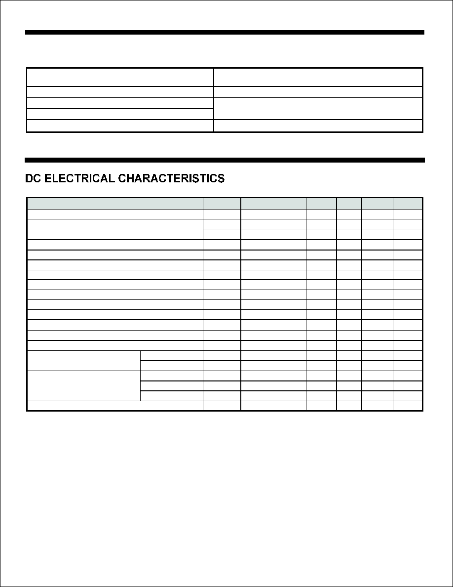
ABSOLUTE MAXIMUM RATINGS
NOTE: Stresses above those listed under "Absolute Maximum Ratings" may cause permanent damage to the device. These are stress ratings only.
Functional operation of the device at these or any other conditions above those indicated in the operational sections of the specifications is not implied.
Exposure to absolute maximum rating conditions for extended periods may affect device reliability.
VDD = 5V ±5%, VEE = -25V, VSS = 0V, TA = operating temperature range (unless otherwise specified).
Voltages referenced to VSS = 0V
Supply Voltage
VDD ..........................0V to 7V
VEE................VDD-35V to 0V
Voltage at any input, except BPIN..-0.3V to VDD+0.3V
Voltage at BPIN input ........... ...VDD-35V to VDD+0.3V
DC current per input pin .....................................10 mA
Power Dissipation............................................500 mW
Operating Temperature Range(Industrial) ....... -40∞C to +85∞C
(Hi-Temp/Mil) ..... -55∞C to +125∞C
Storage Temperature .................................... -65∞C to +125∞C
Solder Temperature (Leads) ..................... +280∞C for 10 sec.
(Package) ........................................ +220∞C
Junction Temperature, Tj .. ........................................ +175∞C
PARAMETER
SYMBOL
CONDITION
MIN
TYP
MAX
UNITS
Operating Voltage
VDD
3.0
7.0
V
Supply Current:
(Converter Off, f
= 0Hz)
IDD
Static, No Load
200
µA
IEE
Static, No Load
120
µA
Input Low Voltage, HI-8050/51 only (except BPIN)
VIL
Logic Inputs
0
0.8
V
Input High Voltage, HI-8050/51 only (except BPIN)
VIH
Logic Inputs
2
VDD
V
Input Low Voltage, BPIN
VILX
VEE
0.6 VDD
V
Input High Voltage, BPIN
VIHX
0.8 VDD
VDD
V
Input Current
(except T1 & T2)
IIN
VIN = 0V to 5V
100
nA
Input Current
(T1 & T2)
IIN
VIN = 0V to 5V
10
Input Capacitance
(Guaranteed, not tested)
CI
10
pF
Segment Output Impedance
RSEG
IL = 10µA
10
15
K
Backplane Output Impedance
RBP
IL = 10µA @ 25∞C
450
600
Data Out Current:
Source Current
IDOH
VOH = 4.5
-3.0
mA
Sink Current
IDOL
VOL = 0.4
3.2
mA
Voltage Converter:
@ No Load
VEE
See Fig. 2
-22
-21.5
-21
V
(VDD - VSS = 5V, TA = 25∞C)
@ 0.1mA Load
IDD
See Fig. 2
1.8
mA
@ 10K
Load
VEE
See Fig. 2
-20
V
Offset Voltage
(Guaranteed, not tested)
VOS
See Fig. 4
25
mV
BP
TTL
TTL
Input Low Voltage, HI-8150/51 only (except BPIN)
VIL
Logic Inputs
0
0.3 VDD
V
Input High Voltage, HI-8150/51 only (except BPIN)
VIH
Logic Inputs
0.7 VDD
VDD
V
µA
CMOS
CMOS
1
2
W
W
W
C
C
HOLT INTEGRATED CIRCUITS
5