
HI-8282A
ARINC 429 SERIAL TRANSMITTER AND DUAL RECEIVER
PIN CONFIGURATION
(Top View)
GENERAL DESCRIPTION
The HI-8282A is a silicon gate CMOS device for interfacing
the ARINC 429 serial data bus to a 16-bit parallel data bus.
Two receivers and an independent transmitter are
provided. The receiver input circuitry and logic are
designed to meet the ARINC 429 specifications for loading,
level detection, timing, and protocol.
The transmitter
section provides the ARINC 429 communication protocol.
Additional interface circuitry such as the Holt HI-8585,
HI-8586 or HI-3182 is required to translate the 5 volt logic
outputs to ARINC 429 drive levels.
The 16-bit parallel data bus exchanges the 32-bit ARINC
data word in two steps when either loading the transmitter
or interrogating the receivers. The data bus interfaces with
CMOS and TTL.
Timing of all the circuitry begins with the master clock input,
CLK. For ARINC 429 applications, the master clock
frequency is 1 MHz.
Each independent receiver monitors the data stream with a
sampling rate 10 times the data rate. The sampling rate is
software selectable at either 1MHz or 125KHz. The results
of a parity check are available as the 32nd ARINC bit. The
HI-8282A examines the null and data timings and will reject
erroneous patterns. For example, with a 125 KHz clock
selection, the data frequency must be between 10.4 KHz
and 15.6 KHz.
The transmitter has a First In, First Out (FIFO) memory to
store 8 ARINC words for transmission. The data rate of the
transmitter is software selectable by dividing the master
clock, CLK, by either 10 or 80. The master clock is used to
set the timing of the ARINC transmission within the required
resolution.
APPLICATIONS
!
!
!
Avionics data communication
Serial to parallel conversion
Parallel to serial conversion
FEATURES
!
!
!
!
!
!
!
!
!
!
!
ARINC specification 429 compliant
16-Bit parallel data bus
Direct receiver interface to ARINC bus
Timing control 10 times the data rate
Selectable data clocks
8 word transmit FIFO
Self test mode
Parity functions
Low power, single 5 volt supply
Industrial & full military temperature ranges
!
!
!
Alternate source to Intersil HS-3282 in all
ARINC 429 applications
Small footprint 44-pin QFP package option
Automatic transmitter data timing
Receiver error rejection per ARINC
specification 429
HOLT INTEGRATED CIRCUITS
www.holtic.com
(DS8282A Rev. D)
02/03
February 2003
44-Pin Plastic Quad Flat Pack (PQFP)
(See page 10 for additional Package Pin Configurations)
44
-
N/C
43
-
429DI2(B)
42
-
429DI2(A)
41
-
429DI1(B)
40
-
429DI1(A)
39
-
VCC
38
-
N/C
37
-
36
-
TXCLK
35
-
CLK
34
-
N/C
MR
33 - N/C
32 - N/C
31 -
30 - ENTX
29 -
28 - 429DO
27 - TX/R
26 -
25 -
24 - BD00
23 - BD01
CWSTRX
429DO
PL2
PL1
N/C
-1
2
BD10
-
1
3
BD09
-1
4
BD08
-1
5
BD07
-1
6
BD06
-1
7
GND
-1
8
BD05
-
1
9
BD04
-2
0
BD03
-
2
1
BD02
-
2
2
N/C - 1
- 2
- 3
SEL - 4
- 5
- 6
BD15 - 7
BD14 - 8
BD13 - 9
BD12 - 10
BD11 - 11
D/R1
D/R2
EN1
EN2
HI-8282APQI
HI-8282APQT
HI-8282APQM

SYMBOL
FUNCTION
DESCRIPTION
VCC
POWER
+5V �5%
429DI1 (A)
INPUT
ARINC receiver 1 positive input
429DI1 (B)
INPUT
ARINC receiver 1 negative input
429DI2 (A)
INPUT
ARINC receiver 2 positive input
429DI2 (B)
INPUT
ARINC receiver 2 negative input
OUTPUT
Receiver 1 data ready flag
OUTPUT
Receiver 2 data ready flag
SEL
INPUT
Receiver data byte selection (0 = BYTE 1) (1 = BYTE 2)
INPUT
Data Bus control, enables receiver 1 data to outputs
INPUT
Data Bus control, enables receiver 2 data to outputs if
is high
BD15
I/O
Data Bus
BD14
I/O
Data Bus
BD13
I/O
Data Bus
BD12
I/O
Data Bus
BD11
I/O
Data Bus
BD10
I/O
Data Bus
BD09
I/O
Data Bus
BD08
I/O
Data Bus
BD07
I/O
Data Bus
BD06
I/O
Data Bus
GND
POWER
0 V
BD05
I/O
Data Bus
BD04
I/O
Data Bus
BD03
I/O
Data Bus
BD02
I/O
Data Bus
BD01
I/O
Data Bus
BD00
I/O
Data Bus
INPUT
Latch enable for byte 1 entered from data bus to transmitter FIFO.
INPUT
Latch enable for byte 2 entered from data bus to transmitter FIFO. Must follow
.
TX/R
OUTPUT
Transmitter ready flag. Goes low when ARINC word loaded into FIFO. Goes high
after transmission and FIFO empty.
429DO
OUTPUT
"ONES" data output from transmitter.
OUTPUT
"ZEROES" data output from transmitter.
ENTX
INPUT
Enable Transmission
INPUT
Clock for control word register
CLK
INPUT
Master Clock input
TX CLK
OUTPUT
Transmitter Clock equal to Master Clock (CLK), divided by either 10 or 80.
INPUT
Master Reset, active low
D/R1
D/R2
EN1
EN2
EN1
PL1
PL2
PL1
429DO
CWSTR
MR
PIN DESCRIPTION
HI-8282A
HOLT INTEGRATED CIRCUITS
2
ARINC 429 DATA FORMAT
The following table shows the bit positions in exchanging data with
the receiver or the transmitter. ARINC bit 1 is the first bit
transmitted or received.
DATA
BD BD BD BD BD BD BD BD BD BD BD BD BD BD BD BD
BUS
15
14
13
12
11
10
09
08
07
06
05
04
03
02
01
00
ARINC
13
12
11
10
9
31
30
32
1
2
3
4
5
6
7
8
BIT
BYTE 1
DATA
BUS
FUNCTION
CONTROL
DESCRIPTION
PIN
If enabled, an internal connection
BDO5
SELF TEST
0 = ENABLE
is made passing 429DO and
to the receiver logic inputs
RECEIVER 1
If enabled, ARINC bits 9 and,
BDO6
DECODER
1 = ENABLE
10 must match the next two
control word bits
If Receiver 1 Decoder is
BDO7
-
-
enabled, the ARINC bit 9
must match this bit
If Receiver 1 Decoder is
BDO8
-
-
enabled, the ARINC bit 10
must match this bit
RECEIVER 2
If enabled, ARINC bits 9 and
BDO9
DECODER
1 = ENABLE
10 must match the next two
control word bits
If Receiver 2 Decoder is
BD10
-
-
enabled, then ARINC bit 9
must match this bit
If Receiver 2 Decoder is
BD11
-
-
enabled, then ARINC bit 10
must match this bit
INVERT
Logic 0 enables normal odd parity
BD12
XMTR
1 = ENABLE
and Logic 1 enables even parity
PARITY
output in transmitter 32nd bit
BD13
XMTR DATA
0 = �10
CLK is divided either by 10 or
CLK SELECT
1 = �80
80 to obtain XMTR data clock
BD14
RCVR DTA
0 = �10
CLK is divided either by 10 or
CLK SELECT
1 = �80
80 to obtain RCVR data clock
429DO
HI-8282A
FUNCTIONAL DESCRIPTION
CONTROL WORD REGISTER
The HI-8282A contains 10 data flip flops whose D inputs are con-
nected to the data bus and clocks connected to
. Each
flip flop provides options to the user as follows:
CWSTR
THE RECEIVERS
ARINC BUS INTERFACE
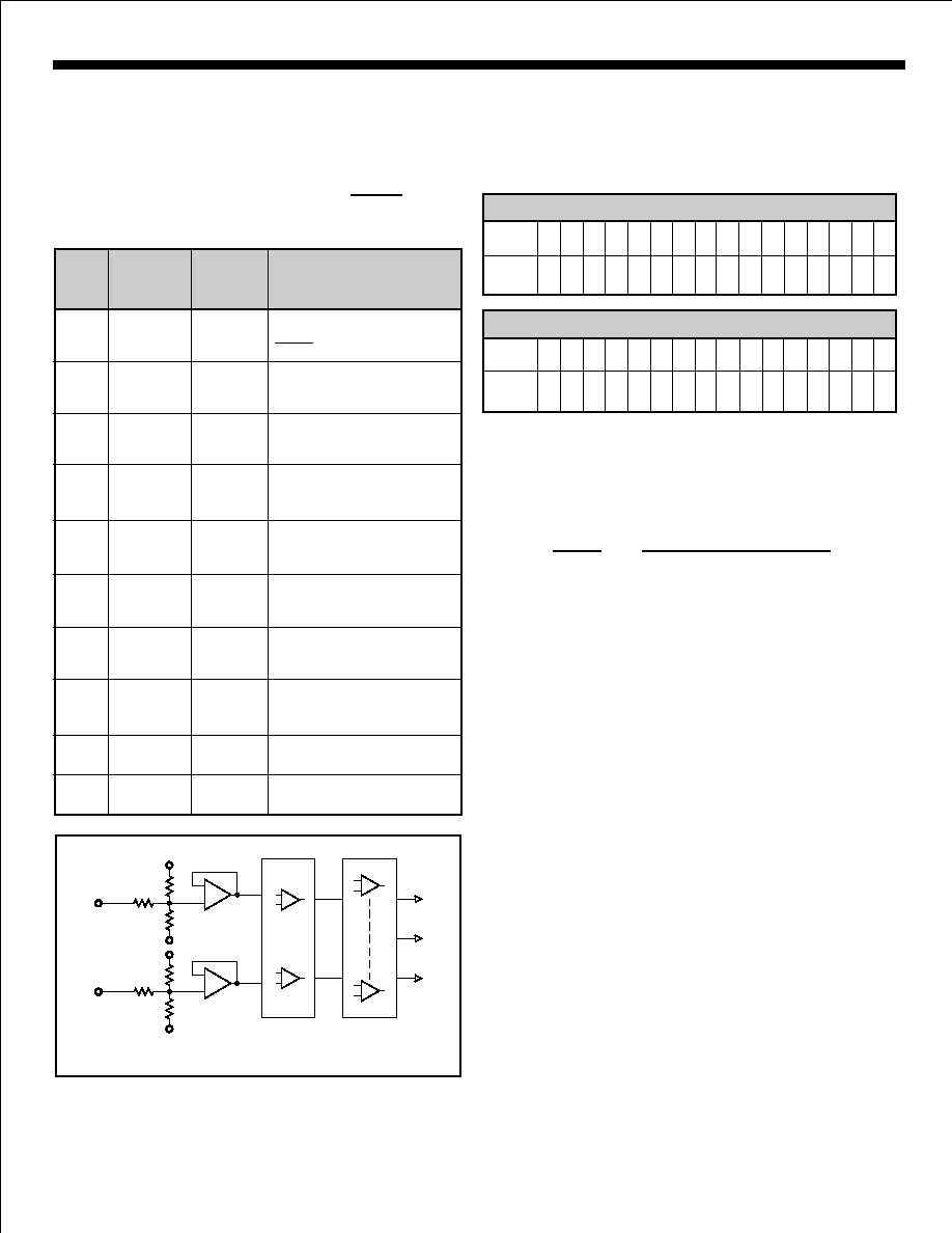
Figure 1 shows the input circuit for each receiver. The ARINC 429
specification requires the following detection levels:
The HI-8282A guarantees recognition of these levels with a common
mode Voltage with respect to GND less than �5V for the worst case
condition (4.75V supply and 13v signal level).
The tolerances in the design guarantee detection of the above
levels, so the actual acceptance ranges are slightly larger. If the
ARINC signal is out of the actual acceptance ranges, including the
nulls, the chip rejects the data.
STATE
DIFFERENTIAL VOLTAGE
ONE
+6.5 Volts to +13 Volts
NULL
+2.5 Volts to -2.5 Volts
ZERO
-6.5 Volts to -13 Volts
HI-8282A-10
The HI-8282A-10 option is similar to the HI-8282A with the exception
that it allows an external 10 Kohm resistor to be added in series with
each ARINC input without affecting the ARINC input thresholds. This
option is especially useful in applications where lightning protection
circuitry is also required.
Each side of the ARINC bus must be connected through a 10 Kohm
series resistor in order for the chip to detect the correct ARINC levels.
The typical 10 volt differential signal is translated and input to a
window comparator and latch. The comparator levels are set so that
with the external 10 Kohm resistors, they are just below the standard
6.5 V minimum ARINC data threshold and just above the 2.5 V
maximum ARINC null threshold.
The receivers of the HI-8282A-10 when used with external
10 Kohm resistors will withstand DO-160D, Level 3, waveforms 3,
4 and 5A. No additional lightning protection circuit is necessary.
Please refer to the Holt AN-300 Application Note for additional
information and recommendations on lightning protection of Holt
Line Drivers and Receivers.
BYTE 2
DATA
BD BD BD BD BD BD BD BD BD BD BD BD BD BD BD BD
BUS
15
14
13
12
11
10
09
08
07
06
05
04
03
02
01
00
ARINC
29
28
27
26
25
24
23
22
21
20
19
18
17
16
15
14
BIT
HOLT INTEGRATED CIRCUITS
3
v
cc
GND
GND
429DI1(B)
OR
429DI2(B)
429DI1(A)
OR
429DI2(A)
DIFFERENTIAL
AMPLIFIERS
ONES
COMPARATORS
NULL
ZEROES
v
cc
FIGURE 1. ARINC RECEIVER INPUT
HI-8282A
RECEIVER LOGIC OPERATION
BIT TIMING
BIT RATE
PULSE RISE TIME
PULSE FALL TIME
PULSE WIDTH
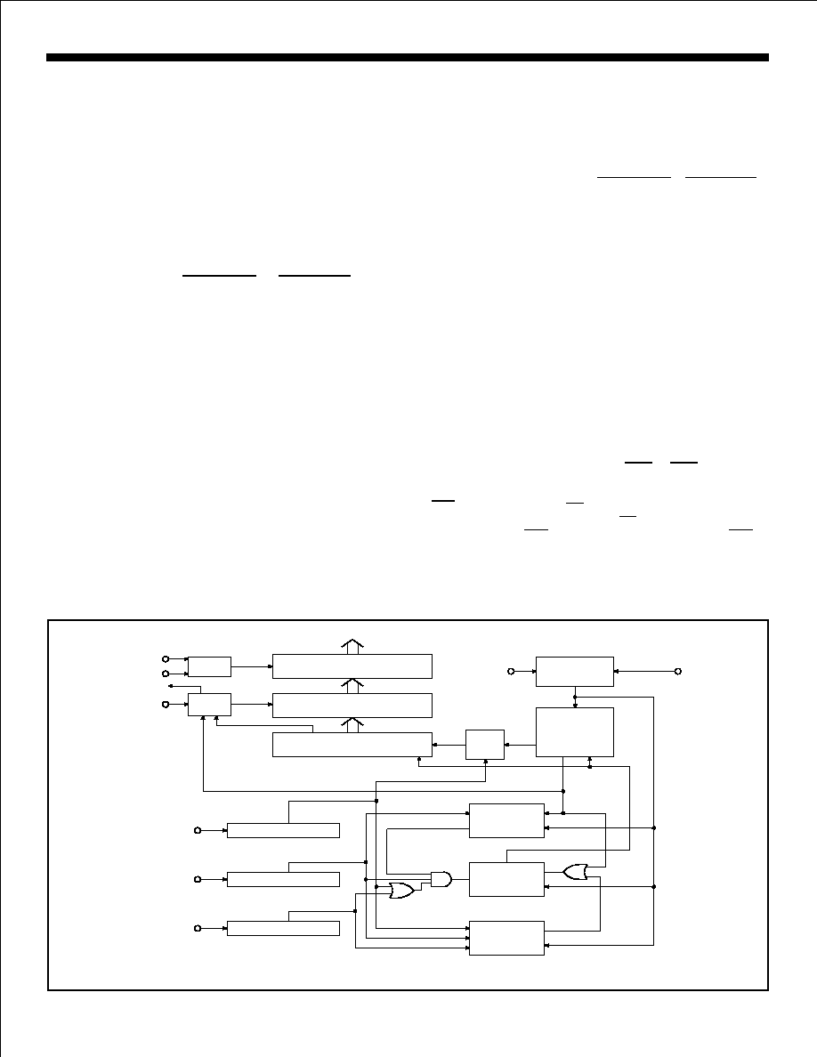
Figure 2 shows a block diagram of the logic section of each re-
ceiver.
The ARINC 429 specification contains the following timing specifi-
cation for the received data:
100K BPS � 1% 12K -14.5K BPS
1.5 � 0.5 �sec
10 � 5 �sec
1.5 � 0.5 �sec
10 � 5 �sec
5 �sec � 5%
34.5 to 41.7 �sec
The HI-8282A accepts signals that meet these specifications and
rejects outside the tolerances.
The way the logic operation
achieves this is described below:
1. Key to the performance of the timing checking logic is an ac-
curate 1MHz clock source. Less than 0.1% error is recom-
mended.
2. The sampling shift registers are 10 bits long and must show
three consecutive Ones, Zeros or Nulls to be considered valid
data. Additionally, for data bits, the One or Zero in the upper
bits of the sampling shift registers must be followed by a Null in
the lower bits within the data bit time.
For a Null in the word
gap, three consecutive Nulls must be found in both the upper
and lower bits of the sampling shift register. In this manner the
minimum pulse width is guaranteed.
HIGH SPEED
LOW SPEED
FUNCTIONAL DESCRIPTION (cont.)
3. Each data bit must follow its predecessor by not less than
8 samples and no more than 12 samples. In this manner the
bit rate is checked. With exactly 1MHz input clock frequency,
the acceptable data bit rates are as follows:
83K BPS
10.4K BPS
125K BPS
15.6K BPS
4. The Word Gap timer samples the Null shift register every
10 input clocks (80 for low speed) after the last data bit of a
valid reception. If the Null is present, the Word Gap counter
is incremented. A count of 3 will enable the next reception.
The receiver parity circuit counts Ones received, including the
parity bit, ARINC bit 32. If the result is odd, then "0" will appear
in the 32nd bit.
HIGH SPEED
LOW SPEED
DATA BIT RATE MIN
DATA BIT RATE MAX
RECEIVER PARITY
RETRIEVING DATA
Once 32 valid bits are recognized, the receiver logic generates
an End of Sequence (EOS). If the receiver decoder is enabled
and the 9th and 10th ARINC bits match the control word pro-
gram bits or if the receiver decoder is disabled, then EOS clocks
the data ready flag flip flop to a "1",
or
(or both) will
go low. The data flag for a receiver will remain low until after
ARINC bytes from that receiver are retrieved. This is ac-
complished by activating
with SEL, the byte selector, low to
retrieve the first byte and activating
with SEL high to retrieve
the second byte.
retrieves data from receiver 1 and
re-
trieves data from receiver 2.
If another ARINC word is received and a new EOS occurs be-
fore the two bytes are retrieved, the data is overwritten by the
new word.
D/R1
D/R2
EN
EN
EN1
EN2
both
SEL
EN
D/R
DECODER
CONTROL
BITS
/
MUX
CONTROL
LATCH
ENABLE
CONTROL
32 TO 16 DRIVER
32 BIT LATCH
32 BIT SHIFT REGISTER
TO PINS
CONTROL
BIT BD14
CLOCK
OPTION
CLOCK
CLK
BIT
COUNTER
AND
END OF
SEQUENCE
PARITY
CHECK
32ND
BIT
DATA
BIT CLOCK
EOS
WORD GAP
WORD GAP
TIMER
BIT CLOCK
END
START
SEQUENCE
CONTROL
ERROR
CLOCK
ERROR
DETECTION
SHIFT REGISTER
SHIFT REGISTER
NULL
ZEROS
SHIFT REGISTER
ONES
EOS
BITS 9 & 10
FIGURE 2.
RECEIVER BLOCK DIAGRAM
HOLT INTEGRATED CIRCUITS
4

HI-8282A
FUNCTIONAL DESCRIPTION (cont.)
TRANSMITTER
A block diagram of the transmitter section is shown in Figure 3.
The FIFO is loaded sequentially by first pulsing
to load byte 1
and then
to load byte 2. The control logic automatically loads
the 31 bit word in the next available position of the FIFO. If TX/R,
the transmitter ready flag, is high (FIFO empty), then 8 words,
each 31 bits long, may be loaded. If TX/R is low, then only the
available positions may be loaded. If all 8 positions are full, the
FIFO ignores further attempts to load data.
When ENTX goes high, enabling transmission, the FIFO
positions are incremented with the top register loading into the
data transmission shift register. Within 2.5 data clocks the first
data bit appears at either 429DO or
. The 31 bits in the
data transmission shift register are presented sequentially to the
outputs in the ARINC 429 format with the following timing:
ARINC DATA BIT TIME
10 Clocks
80 Clocks
DATA BIT TIME
5 Clocks
40 Clocks
NULL BIT TIME
5 Clocks
40 Clocks
WORD GAP TIME
40 Clocks
320 Clocks
The word counter detects when all loaded positions are trans-
mitted and sets the transmitter ready flag, TX/R, high.
FIFO OPERATION
DATA TRANSMISSION
PL1
PL2
429DO
HIGH SPEED
LOW SPEED
TRANSMITTER PARITY
The parity generator counts the ONES in the 31-bit word. If the
BD12 control word bit is set low, the 32nd bit transmitted will
make parity odd. If the control bit is high, the parity is even.
The two receivers are independent of the transmitter. Therefore,
control of data exchanges is strictly at the option of the user. The
only restrictions are:
1. The received data may be overwritten if not retrieved
within one ARINC word cycle.
2. The FIFO can store 8 words maximum and ignores
attempts to load addition data if full.
3. Byte 1 of the transmitter data must be loaded first.
4. Either byte of the received data may be retrieved first.
Both bytes must be retrieved to clear the data ready flag.
5. After ENTX, transmission enable, goes high it cannot go
low until TX/R, transmitter ready flag, goes high. Otherwise,
one ARINC word is lost during transmission.
SELF TEST
SYSTEM OPERATION
If the BD05 control word bit is set low, 429DO or
are
internally connected to the receivers inputs, bypassing the
interface circuitry. Data to Receiver 1 is as transmitted and data to
Recevier 2 is the complement. 429DO and
outputs remain
active during self test.
429DO
429DO
FIGURE 3.
TRANSMITTER BLOCK DIAGRAM
BIT BD12
DATA
CLOCK
CONTROL BIT
BD13
PL1
PL2
CLK
TX CLK
PARITY
GENERATOR
DATA AND
NULL TIMER
SEQUENCER
BIT
AND
WORD GAP
COUNTER
START
SEQUENCE
WORD COUNTER
AND
FIFO CONTROL
INCREMENT
WORD COUNT
DATA CLOCK
DIVIDER
FIFO
LOADING
SEQUENCER
429DO
429DO
8 X 31 FIFO
31 BIT PARALLEL
LOAD SHIFT REGISTER
BIT CLOCK
WORD CLOCK
ADDRESS
LOAD
DATA BUS
TX/R
ENTX
HOLT INTEGRATED CIRCUITS
5