HI-8282
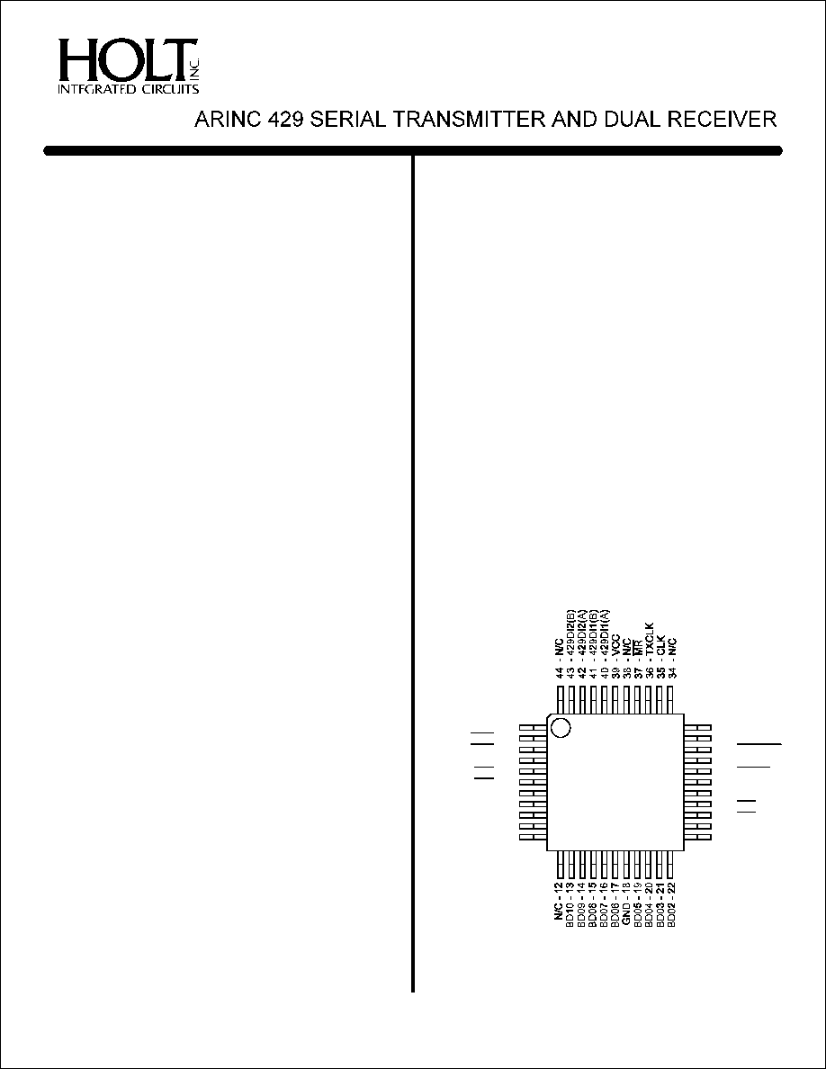
PIN CONFIGURATION
(Top View)
GENERAL DESCRIPTION
The HI-8282 is a silicon gate CMOS device for interfacing
the ARINC 429 serial data bus to a 16-bit parallel data bus.
Two receivers and an independent transmitter are
provided. The receiver input circuitry and logic are
designed to meet the ARINC 429 specifications for loading,
level detection, timing, and protocol.
The transmitter
section provides the ARINC 429 communication protocol.
Additional interface circuitry such as the Holt HI-8382 is
required to translate the 5 volt logic outputs to ARINC 429
drive levels.
The 16-bit parallel data bus exchanges the 32-bit ARINC
data word in two steps when either loading the transmitter
or interrogating the receivers. The data bus interfaces with
CMOS and TTL.
Timing of all the circuitry begins with the master clock input,
CLK. For ARINC 429 applications, the master clock
frequency is 1 MHz.
Each independent receiver monitors the data stream with a
sampling rate 10 times the data rate. The sampling rate is
software selectable at either 1MHz or 125KHz. The results
of a parity check are available as the 32nd ARINC bit. The
HI-8282 examines the null and data timings and will reject
erroneous patterns. For example, with a 125 KHz clock
selection, the data frequency must be between 10.4 KHz
and 15.6 KHz.
The transmitter has a First In, First Out (FIFO) memory to
store 8 ARINC words for transmission. The data rate of the
transmitter is software selectable by dividing the master
clock, CLK, by either 10 or 80. The master clock is used to
set the timing of the ARINC transmission within the required
resolution.
APPLICATIONS
!
!
!
Avionics data communication
Serial to parallel conversion
Parallel to serial conversion
FEATURES
!
!
!
!
!
!
!
!
!
!
!
ARINC specification 429 compatible
16-Bit parallel data bus
Direct receiver interface to ARINC bus
Timing control 10 times the data rate
Selectable data clocks
Receiver error rejection per ARINC
specification 429
Automatic transmitter data timing
Self test mode
Parity functions
Low power, single 5 volt supply
Industrial & full military temperature ranges
!
DESC SMD part number
HOLT INTEGRATED CIRCUITS
4-29
(DS8282 Rev. A)
01/01
January 2001
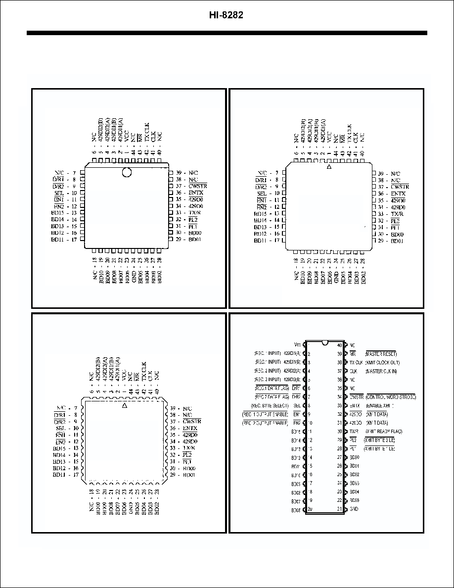
44-Pin Plastic Quad Flat Pack (PQFP)
(See page 4-38 for additional Package Pin Configurations)
33 - N/C
32 - N/C
31 -
30 - ENTX
29 -
28 - 429DO
27 - TX/R
26 -
25 -
24 - BD00
23 - BD01
CWSTRX
429DO
PL2
PL1
N/C - 1
- 2
- 3
SEL - 4
- 5
- 6
BD15 - 7
BD14 - 8
BD13 - 9
BD12 - 10
BD11 - 11
D/R1
D/R2
EN1
EN2
HI-8282PQI
&
HI-8282PQT
SYMBOL
FUNCTION
DESCRIPTION
VCC
POWER
+5V ±5%
429DI1 (A)
INPUT
ARINC receiver 1 positive input
429DI1 (B)
INPUT
ARINC receiver 1 negative input
429DI2 (A)
INPUT
ARINC receiver 2 positive input
429DI2 (B)
INPUT
ARINC receiver 2 negative input
OUTPUT
Receiver 1 data ready flag
OUTPUT
Receiver 2 data ready flag
SEL
INPUT
Receiver data byte selection (0 = BYTE 1) (1 = BYTE 2)
INPUT
Data Bus control, enables receiver 1 data to outputs
INPUT
Data Bus control, enables receiver 2 data to outputs if
is high
BD15
I/O
Data Bus
BD14
I/O
Data Bus
BD13
I/O
Data Bus
BD12
I/O
Data Bus
BD11
I/O
Data Bus
BD10
I/O
Data Bus
BD09
I/O
Data Bus
BD08
I/O
Data Bus
BD07
I/O
Data Bus
BD06
I/O
Data Bus
GND
POWER
0 V
BD05
I/O
Data Bus
BD04
I/O
Data Bus
BD03
I/O
Data Bus
BD02
I/O
Data Bus
BD01
I/O
Data Bus
BD00
I/O
Data Bus
INPUT
Latch enable for byte 1 entered from data bus to transmitter FIFO.
INPUT
Latch enable for byte 2 entered from data bus to transmitter FIFO. Must follow
TX/R
OUTPUT
Transmitter ready flag. Goes low when ARINC word loaded into FIFO. Goes high
after transmission and FIFO empty.
429DO
OUTPUT
"ONES" data output from transmitter.
OUTPUT
"ZEROES" data output from transmitter.
ENTX
INPUT
Enable Transmission
INPUT
Clock for control word register
CLK
INPUT
Master Clock input
TX CLK
OUTPUT
Transmitter Clock equal to Master Clock (CLK), divided by either 10 or 80.
INPUT
Master Reset, active low
D/R1
D/R2
EN1
EN2
EN1
PL1
PL2
PL1.
429DO
CWSTR
MR
PIN DESCRIPTION
HI-8282
HOLT INTEGRATED CIRCUITS
4-30
FUNCTIONAL DESCRIPTION
DATA
BUS
FUNCTION
CONTROL
DESCRIPTION
PIN
If enabled, an internal connection
BDO5
SELF TEST
0 = ENABLE
is made passing 429DO and
to the receiver logic inputs
RECEIVER 1
If enabled, ARINC bits 9 and,
BDO6
DECODER
1 = ENABLE
10 must match the next two
control word bits
If Receiver 1 Decoder is
BDO7
-
-
enabled, the ARINC bit 9
must match this bit
If Receiver 1 Decoder is
BDO8
-
-
enabled, the ARINC bit 10
must match this bit
RECEIVER 2
If enabled, ARINC bits 9 and
BDO9
DECODER
1 = ENABLE
10 must match the next two
control word bits
If Receiver 2 Decoder is
BD10
-
-
enabled, then ARINC bit 9
must match this bit
If Receiver 2 Decoder is
BD11
-
-
enabled, then ARINC bit 10
must match this bit
INVERT
Logic 0 enables normal odd parity
BD12
XMTR
1 = ENABLE
and Logic 1 enables even parity
PARITY
output in transmitter 32nd bit
BD13
XMTR DATA
0 = ˜10
CLK is divided either by 10 or
CLK SELECT
1 = ˜80
80 to obtain XMTR data clock
BD14
RCVR DTA
0 = ˜10
CLK is divided either by 10 or
CLK SELECT
1 = ˜80
80 to obtain RCVR data clock
429DO
CONTROL WORD REGISTER
The HI-8282 contains 10 data flip flops whose D inputs are con-
nected to the data bus and clocks connected to
. Each
flip flop provides options to the user as follows:
CWSTR
THE RECEIVERS
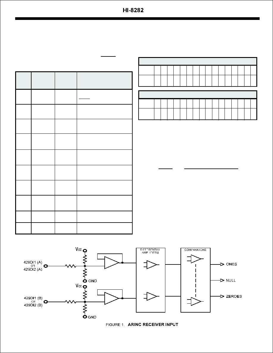
ARINC BUS INTERFACE
Figure 1 shows the input circuit for each receiver. The ARINC 429
specification requires the following detection levels:
The HI-8282 guarantees recognition of these levels with a common
mode Voltage with respect to GND less than ±4V for the worst case
condition (4.75V supply and 13v signal level).
The tolerances in the design guarantee detection of the above
levels, so the actual acceptance ranges are slightly larger. If the
ARINC signal is out of the actual acceptance ranges, including the
nulls, the chip rejects the data.
STATE
DIFFERENTIAL VOLTAGE
ONE
+6.5 Volts to +13 Volts
NULL
+2.5 Volts to -2.5 Volts
ZERO
-6.5 Volts to -13 Volts
BYTE 2
DATA
BD BD BD BD BD BD BD BD BD BD BD BD BD BD BD BD
BUS
15
14
13
12
11
10
09
08
07
06
05
04
03
02
01
00
ARINC
29
28
27
26
25
24
23
22
21
20
19
18
17
16
15
14
BIT
ARINC 429 DATA FORMAT
The following table shows the bit positions in exchanging data with
the receiver or the transmitter. ARINC bit 1 is the first bit
transmitted or received.
DATA
BD BD BD BD BD BD BD BD BD BD BD BD BD BD BD BD
BUS
15
14
13
12
11
10
09
08
07
06
05
04
03
02
01
00
ARINC
13
12
11
10
9
31
30
32
1
2
3
4
5
6
7
8
BIT
BYTE 1
HOLT INTEGRATED CIRCUITS
4-31

HI-8282
RECEIVER LOGIC OPERATION
BIT TIMING
BIT RATE
PULSE RISE TIME
PULSE FALL TIME
PULSEWIDTH
Figure 2 shows a block diagram of the logic section of each receiver.
The ARINC 429 specification contains the following timing
specification for the received data:
100K BPS ± 1%
12K -14.5K BPS
1.5 ± 0.5 µsec
10 ± 5 µsec
1.5 ± 0.5 µsec
10 ± 5 µsec
5 µsec ± 5%
34.5 to 41.7 µsec
Again the HI-8282 accepts signals that meet these specifications
and rejects outside the tolerances. The way the logic operation
achieves this is described below:
1. Key to the performance of the timing checking logic is an ac-
curate 1MHz clock source.
Less than 0.1% error is
recommmended.
2. The sampling shift registers are 10 bits long and must show
three consecutive Ones, Zeros or Nulls to be considered valid
data. Additionally, for data bits, the One or Zero in the upper bits
of the sampling shift registers must be followed by a Null in the
lower bits within the data bit time. For a Null in the word gap,
three consecutive Nulls must be found in both the upper and
lower bits of the sampling shift register. In this manner the mini-
mum pulse width is guaranteed.
HIGH SPEED
LOW SPEED
FUNCTIONAL DESCRIPTION (con't)
3. Each data bit must follow its predecessor by not less than
8 samples and no more than 12 samples. In this manner the
bit rate is checked. With exactly 1MHz input clock frequency,
the acceptable data bit rates are as follows:
83K BPS
10.4K BPS
125K BPS
15.6K BPS
4. The Word Gap timer samples the Null shift register every
10 input clocks (80 for low speed) after the last data bit of a
valid reception. If the Null is present, the Word Gap counter is
incremented. A count of 3 will enable the next reception.
The receiver parity circuit counts Ones received, including the
parity bit, ARINC bit 32. If the result is odd, then "0" will appear in
the 32nd bit.
HIGH SPEED
LOW SPEED
DATA BIT RATE MIN
DATA BIT RATE MAX
RECEIVER PARITY
RETRIEVING DATA
Once 32 valid bits are recognized, the receiver logic generates
an End of Sequence (EOS). If the receiver decoder is enabled
and the 9th and 10th ARINC bits match the control word
program bits or if the receiver decoder is disabled, then EOS
clocks the data ready flag flip flop to a "1",
or
(or both)
will go low. The data flag for a receiver will remain low until after
ARINC bytes from that receiver are retrieved.
This is
accomplished by activating
with SEL, the byte selector, low
to retrieve the first byte and activating
with SEL high to
retrieve the second byte.
retrieves data from receiver 1 and
retrieves data from receiver 2.
If another ARINC word is received, and a new EOS occurs
before the two bytes are retrieved, the data is overwritten by the
new word.
D/R1
D/R2
EN
EN
ENI
EN2
both
SEL
EN
D/R
DECODER
CONTROL
BITS
/
MUX
CONTROL
LATCH
ENABLE
CONTROL
32 TO 16 DRIVER
32 BIT LATCH
32 BIT SHIFT REGISTER
TO PINS
CONTROL
BIT BD14
CLOCK
OPTION
CLOCK
CLK
BIT
COUNTER
AND
END OF
SEQUENCE
PARITY
CHECK
32ND
BIT
DATA
BIT CLOCK
EOS
WORD GAP
WORD GAP
TIMER
BIT CLOCK
END
START
SEQUENCE
CONTROL
ERROR
CLOCK
ERROR
DETECTION
SHIFT REGISTER
SHIFT REGISTER
NULL
ZEROS
SHIFT REGISTER
ONES
EOS
BITS 9 & 10
FIGURE 2.
RECEIVER BLOCK DIAGRAM
HOLT INTEGRATED CIRCUITS
4-32

TRANSMITTER
A block diagram of the transmitter section is shown in Figure 3.
The FIFO is loaded sequentially by first pulsing
to load byte 1
and then
to load byte 2. The control logic automatically loads
the 31 bit word in the next available position of the FIFO. If TX/R,
the transmitter ready flag is high (FIFO empty), then 8 words,
each 31 bits long, may be loaded. If TX/R is low, then only the
available positions may be loaded. If all 8 positions are full, the
FIFO ignores further attempts to load data.
When ENTX goes high, enabling transmission, the FIFO
positions are incremented with the top register loading into the
data transmission shift register. Within 2.5 data clocks the first
data bit appears at either 429DO or
. The 31 bits in the
data transmission shift register are presented sequentially to the
outputs in the ARINC 429 format with the following timing:
ARINC DATA BIT TIME
10 Clocks
80 Clocks
DATA BIT TIME
5 Clocks
40 Clocks
NULL BIT TIME
5 Clocks
40 Clocks
WORD GAP TIME
40 Clocks
320 Clocks
The word counter detects when all loaded positions are
transmitted and sets the transmitter ready flag, TX/R, high.
FIFO OPERATION
DATA TRANSMISSION
PL1
PL2
429DO
HIGH SPEED
LOW SPEED
TRANSMITTER PARITY
The parity generator counts the ONES in the 31-bit word. If the
BD12 control word bit is set low, the 32nd bit transmitted will make
parity odd. If the control bit is high the parity is even.
If the BD05 control word bit is set low, 429DO or
become
inputs to the receiver bypassing the interface circuitry.
The two receivers are independent of the transmitter. Therefore,
control of data exchanges are strictly at the option of the user. The
only restrictions are:
1. The received data may be overwritten if not retrieved
within one ARINC word cycle.
2. The FIFO can store 8 words maximum and ignores
attempts to load addition data if full.
3. Byte 1 of the transmitter data must be loaded first.
4. Either byte of the received data may be retrieved first.
Both bytes must be retrieved to clear the data ready flag.
5. After ENTX, transmission enable, goes high it cannot go
low until TX/R, transmitter readyflag, goes high. Otherwise,
one ARINC word is lost during transmission.
SELF TEST
SYSTEMOPERATION
429DO
HOLT INTEGRATED CIRCUITS
4-33

REPEATER OPERATION
The repeater mode of operation allows a data word that has been
received by the HI-8282 to be placed directly into its FIFO for
transmission. After a 32-bit word has been shifted into the receiver
shift register, the
flag will go low. A logic "0" is placed on the SEL
line and
is strobed. This is the same procedure as for normal
receiver operation and it places the lower byte (16) of the data word
o n
t h e
d a t a
b u s .
B y
s t r o b i n g
a t
t h e
s a m e
D/R
EN
P L 1
HI-8282
time as
, the byte will also be placed into the transmitter FIFO.
SEL is then taken high and
is strobed again to place the upper
byte of the data word on the data bus. By strobing
at the same
time as
, the second byte will also be placed into the FIFO. The
data word is now ready to be transmitted according to the parity
programmed into the control word register.
In normal operation, either byte of a received data word may be read
from the receiver latches first by use of SEL input. During repeater
operation however, the lower byte of the data word must be read
first. This is necessary because, as the data is being read, it is also
being loaded into the FIFO and the transmitter FIFO is always
loaded with the lower byte of the data word first.
EN
EN
PL2
EN
429DO
429DO
ARINC BIT
NULL
DATA
DATA
DATA
NULL
NULL
WORD GAP
BIT 1
NEXT WORD
BIT 32
BIT 31
BIT 30
CWHLD
t
CWSET
t
CWSTR
t
DATA BUS
CWSTR
VALID
DATA BUS
SELEN
t
D/R
t
ENSEL
t
DATAEN
t
D/REN
t
END/R
t
EN
t
ENSEL
t
SELEN
t
DATAEN
t
ENDATA
t
ENDATA
t
ENEN
t
BYTE 1 VALID
BYTE 2 VALID
HOLT INTEGRATED CIRCUITS
4-34

HI-8282
PL2
DWSET
t
DWHLD
t
TX/R
t
DWHLD
t
PL12
t
PL
t
DATA BUS
PL1
TX/R
BYTE 2 VALID
PL
t
PL12
t
DWSET
t
BYTE 1 VALID
ARINC BIT
429DO
or
429DO
PL2
ENTX
TX/R
PL2EN
t
ENDAT
t
DTX/R
t
ENTX/R
t
DATA
BIT 1
DATA
BIT 2
DATA
BIT 32
DON'T CARE
429DI
D/R
EN
PL1
PL2
SEL
TX/R
ENTX
429DO
BIT 32
DON'T CARE
D/R
t
EN
t
D/REN
t
ENEN
t
EN
t
END/R
t
SELEN
t
ENSEL
t
ENPL
t
PLEN
t
SELEN
t
ENSEL
t
ENPL
t
PLEN
t
TX/R
t
TX/REN
t
ENDAT
t
ENTX/R
t
DTX/R
t
NULL
t
BIT 1
BIT 32
HOLT INTEGRATED CIRCUITS
4-35

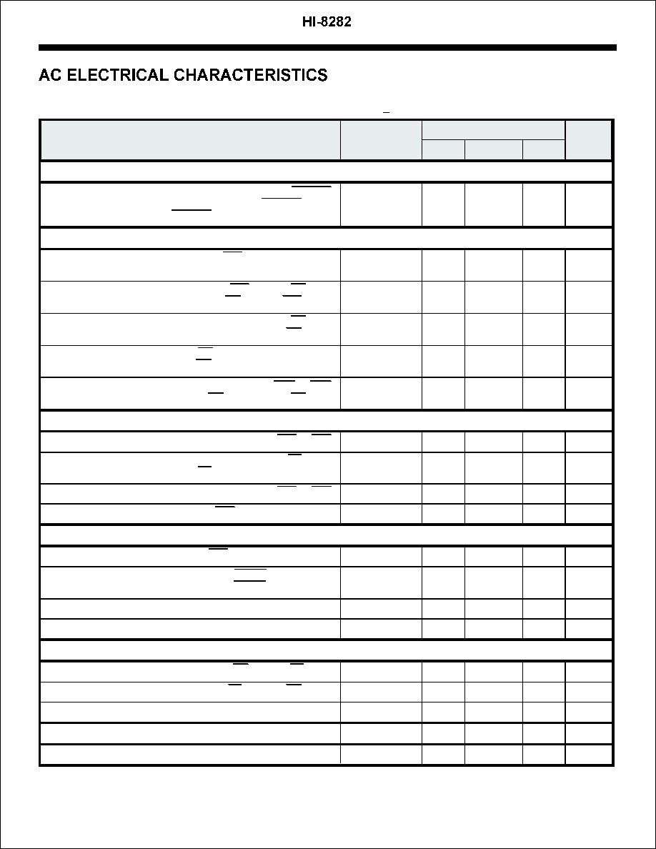
LIMITS
PARAMETER
CONDITIONS
UNIT
SYMBOL
Differential Input Voltage:
ONE
V
Pins 2 to 3, 4 to 5: Common
6.5
10.0
13.0
V
ZERO
V
mode voltage less than ±4V
-13.0
-10.0
-6.5
V
NULL
V
with respect to GND
-2.5
0
2.5
V
Input Resistance:
Differential
R
12
K
To GND
R
12
27
K
To Vcc
R
12
27
k
Input Current:
Input Sink
I
200
µA
Input Source
I
-450
µA
Input Capacitance:
Differential
C
Pins 2 to 3, 4 to 5
20
pF
(Guaranteed but not tested)
To GND
C
20
pF
To Vcc
C
20
pF
Input Voltage:
Input Voltage HI
V
2.1
V
Input Voltage LO
V
0.7
V
Input Current:
Input Sink
I
1.5
µA
Input Source
I
-1.5
µA
Input Voltage:
Input Voltage HI
V
3.5
V
Input Voltage LO
V
0.7
V
Input Current:
Input Sink
I
10
µA
Input Source
I
-20
µA
Output Voltage:
Logic "1" Output Voltage
V
I
= -1.5mA
2.7
V
Logic "0" Output Voltage
V
I
= 1.8mA
0.4
V
Output Current:
Output Sink
I
V
= 0.4V
3.0
mA
(Bi-directional Pins)
Output Source
I
V
= V
- 0.4V
1.5
mA
Output Current:
Output Sink
I
V
= 0.4V
3.6
mA
(All Other Outputs)
Output Source
I
V
= V
- 0.4V
1.5
mA
Output Capacitance:
C
15
pF
Standby Supply Current:
I
20
mA
Operating Supply Current:
I
20
mA
MIN
TYP
MAX
ARINC INPUTS
-
Pins 2, 3, 4 & 5
BI-DIRECTIONAL INPUTS - Pins 11 - 20, 22 - 27
ALL OTHER INPUTS - Pins 8 - 10, 28, 29, 33, 34, 37, 39
OUTPUTS - Pins 6, 7, 11 - 20, 22 - 27, 30 - 32, 38
SUPPLY INPUT - Pin 1
IH
IL
NUL
I
G
H
IH
IL
I
G
H
IH
IL
IH
IL
IH
IL
IH
IL
OH
OH
OL
OL
OL
OUT
OH
OUT
CC
OL
OUT
OH
OUT
CC
O
CC1
CC2
W
W
W
Vcc = 5V ±5%, GND = 0V, TA = Operating Temperature Range (unless otherwise specified).
Power Dissipation
500mW
Operating Temperature Range: (Industrial)
-40∞C to +85∞C
(Military)
-55∞C to +125∞C
Storage Temperature Range:
-65∞C to +150∞C
Supply Voltage Vcc
-0.3V to +7V
Voltage at pins 2, 3, 4 & 5
-29V to +29V
Voltage at any other pin
-0.3V to Vcc +0.3V
DC Current Drain per input pin
10mA
NOTE: Stresses above those listed under "Absolute Maximum Ratings" may cause permanent damage to the device. These are stress ratings only.
Functional operation of the device at these or any other conditions above those indicated in the operational sections of the specifications is not implied.
Exposure to absolute maximum rating conditions for extended periods may affect device reliability.
HOLT INTEGRATED CIRCUITS
4-36
LIMITS
PARAMETER
SYMBOL
UNITS
MIN
TYP
MAX
CONTROL WORD TIMING
RECEIVER TIMING
FIFO TIMING
TRANSMISSION TIMING
REPEATER OPERATION TIMING
Master Reset Pulse Width
ARINC Data Rate and Bit Timing
Pulse Width -
t
130
ns
Setup - DATA BUS Valid to
HIGH
t
140
ns
Hold -
HIGH to DATA BUS Hi-Z
t
0
ns
Delay - Start ARINC 32nd Bit to
LOW: High Speed
t
16
µs
Low Speed
t
128
µs
Delay -
LOW to
L0W
t
0
ns
Delay -
LOW to
HIGH
t
200
ns
Setup - SEL to
L0W
t
20
ns
Hold - SEL to
HIGH
t
50
ns
Delay -
L0W to DATA BUS Valid
t
200
ns
Delay -
HIGH to DATA BUS Hi-Z
t
30
ns
Pulse Width -
or
t
240
ns
Spacing -
HIGH to next
L0W
t
50
ns
Pulse Width -
or
t
200
ns
Setup - DATA BUS Valid to
HIGH
t
110
ns
Hold -
HIGH to DATA BUS Hi-Z
t
20
ns
Spacing -
or
t
0
ns
Delay -
HIGH to TX/R LOW
t
840
ns
Spacing -
HIGH to ENTX HIGH
t
0
µs
Delay - ENTX HIGH to 429DO or
: High Speed
t
25
µs
Delay - ENTX HIGH to 429DO or
: Low Speed
t
200
µs
Delay - 32nd ARINC Bit to TX/R HIGH
t
400
ns
Spacing - TX/R HIGH to ENTX L0W
t
0
ns
Delay -
LOW to
LOW
t
0
ns
Hold -
HIGH to
HIGH
t
0
ns
Delay - TX/R LOW to ENTX HIGH
t
0
ns
t
400
ns
± 1%
CWSTR
CWSTR
CWSTR
D/R
D/R
EN
EN
D/R
EN
EN
EN
EN
EN1
EN2
EN
EN
PL1
PL2
PL
PL
PL1
PL2
PL2
PL2
429D0
429D0
EN
PL
PL
EN
CWSTR
CWSET
CWHLD
D/R
D/R
D/REN
END/R
SELEN
ENSEL
ENDATA
DATAEN
EN
ENEN
PL
DWSET
DWHLD
PL12
TX/R
PL2EN
ENDAT
ENDAT
DTX/R
ENTX/R
ENPL
PLEN
TX/REN
MR
HOLT INTEGRATED CIRCUITS
4-37
Vcc = 5V, GND = 0V, TA = Operating Temperature Range and fclk = 1mhz 0.1% with 60/40 duty cycle
+
ADDITIONAL HI-8282 PIN CONFIGURATIONS
(See page 4-29 for the 44-pin Plastic Quad Flat Pack )
HOLT INTEGRATED CIRCUITS
4-38
HI-8282C
HI-8282J-44
HI-8282U
44-PIN J-LEAD CERQUAD
44-PIN CERAMIC LCC
HI-8282S
40-PIN CERAMIC SIDE BRAZED DIP
44-PIN PLASTIC PLCC
PART
NUMBER
DESCRIPTION
TEMPERATURE
RANGE
FLOW BURN
IN
LEAD
FINISH
HI-8282C
40 PIN CERAMIC SIDE BRAZED DIP
-40∞C TO +85∞C
I
NO
GOLD
HI-8282CT
40 PIN CERAMIC SIDE BRAZED DIP
-55∞C TO +125∞C
T
NO
GOLD
HI-8282CM-01 40 PIN CERAMIC SIDE BRAZED DIP
-55∞C TO +125∞C
M
YES
SOLDER
HI-8282CM-03* 40 PIN CERAMIC SIDE BRAZED DIP
-55∞C TO +125∞C
DSCC
YES
SOLDER
HI-8282J-44
44 PIN PLASTIC J LEAD
-40∞C TO +85∞C
I
NO
SOLDER
HI-8282JT-44
44 PIN PLASTIC J LEAD
-55∞C TO +125∞C
T
NO
SOLDER
HI-8282PQI
44 PIN PLASTIC QUAD FLAT PACK
-40∞C TO +85∞C
I
NO
SOLDER
HI-8282PQT
44 PIN PLASTIC QUAD FLAT PACK
-55∞C TO +125∞C
T
NO
SOLDER
HI-8282S
44 PIN CERAMIC LEADLESS CHIP CARRIER -40∞C TO +85∞C
I
NO
GOLD
HI-8282ST
44 PIN CERAMIC LEADLESS CHIP CARRIER -55∞C TO +125∞C
T
NO
GOLD
HI-8282SM-01 44 PIN CERAMIC LEADLESS CHIP CARRIER -55∞C TO +125∞C
M
YES
SOLDER
HI-8282U
44 PIN CERQUAD
-40∞C TO +85∞C
I
NO
SOLDER
HI-8282UT
44 PIN CERQUAD
-55∞C TO +125∞C
T
NO
SOLDER
HI-8282
* SMD# 5962-8688002QA
HOLT INTEGRATED CIRCUITS
4-39
PACKAGE

Package Type:
2 1 44 43
.620
±
.012
(15.748
±
.305)
.688
±
.005
(17.475
±
.127)
MAX.
.650
(16.510
.254)
SQ.
.200
(5.080)MAX.
.050
(1.270)
.019
±
±
.051)
.100
.007
(2.540
±
44-PIN J-LEAD CERQUAD
44U
.039
±
.005
(.990
±
.127)
Package Type:
2.020 MAX
(51.308 MAX)
.225 MAX
(5.715 MAX)
.100 BSC
(2.540 BSC)
.018 TYP
(.457 TYP)
.050 TYP
(1.270 TYP)
.085
±
.009
(2.159
±
.229)
.125 MIN
(3.175 MIN)
.610
±
.010
(15.494
±
.254)
.600
±
.010
(15.240
±
.254)
.595
±
.010
(15.113
±
.254)
.010
+
.002
/-
.001
(.254
+
.051
/-
.025)
40-PIN CERAMIC SIDE-BRAZED DIP
40C
HI-8282 PACKAGE DIMENSIONS
inches (millimeters)
HOLT INTEGRATED CIRCUITS
1

Package Type:
PIN NO. 1 IDENT
.045 x 45∞
.050
±
.005
(1.27
±
.127)
.045 x 45∞
PIN NO. 1
44-PIN PLASTIC PLCC
SEE DETAIL
A
.172
±
.008
(4.369
±
.203)
DETAIL A
.020 MIN
(.508
)
.025
.045
R
.690
±
.005
(17.526
±
.127)
SQ.
.610
±
.020
(15.494
±
.508)
.031
±
.005
(.787
±
.127)
.653
±
.004
(16.586
±
.102)
SQ.
.017
±
.004
(.432
±
.102)
.015 ± .002
(.381
±
.051)
.009
.011
44J
HI-8282 PACKAGE DIMENSIONS
inches (millimeters)
HOLT INTEGRATED CIRCUITS
2
Package Type:
0
∞
7
∞
Detail A
See Detail A
SQ.
44PQS
44-PIN PLASTIC QUAD FLAT PACK (PQFP)
.007
(.17)
.547 ± .010
(13.90 ± .25)
.394 ± .004
(10.0 ± .10)
SQ.
MAX.
.014 ± ..002
(.35 ± .05)
.035 +.006 / -.004
(.88 +.15 / -.10)
.008
(.20 R)
TYP.
.012
(.30 R)
TYP.
.079 +.004 / -.006
(2.00 +.10 / -.15)
.097
(2.45)
MAX.
.0315 BSC
(.80 BSC)

Package Type:
44-PIN CERAMIC LEADLESS CHIP CARRIER
44S
.651
±
.011
(16.535
±
.279)
SQ.
.075
±
.004
(1.905
±
.101)
.326
±
.006
(8.280
±
.152)
PIN 1
.050 BSC
(1.270 BSC)
.009R ± .006
(.229R
±
.152)
.092
± .
028
(2.336
±
.711)
.025
±
.003
(.635
±
.076)
.050
± .
005
(1.270
±
.127)
.020 INDEX
(.508 INDEX)
.040 x 45∞ 3 PLCS
(1.016 x 45∞ 3 PLCS)
PIN 1
HI-8282 PACKAGE DIMENSIONS
inches (millimeters)
HOLT INTEGRATED CIRCUITS
3