
HOLT INTEGRATED CIRCUITS
www.holtic.com
HI-8422
16-Channel Discrete-to-Digital Interface
Sensing 28 Volt / Open and Open / Ground Signals
DESCRIPTION
FEATURES
PIN CONFIGURATION
The HI-8422 is a sixteen channel discrete-to-digital
interface device. The device has eight channels designed
to sense 28 V / Open signals and eight channels that sense
Open / Ground signals. Data is multiplexed from each bank
of sensors to an eight bit digital databus. Mixed-signal
CMOS technology is used to provide superior low-power
performance. The device outputs are CMOS / TTL
compatible and may be disabled (tri-state) using the
and
pins.
The HI-8422 is offered in a small footprint 32-pin Plastic
Quad Flat Package (PQFP). Please contact the Holt sales
department for other packaging options.
CE
OE
!
!
!
!
!
!
8 independent 28 Volt / Open sensing channels
8 independent Open / Ground sensing channels
5.0 V single supply operation
Low power CMOS technology
Sense inputs are internally lightning protected per
DO-160D level 3
Military processing options available
February 2003
(DS8422 Rev. C)
02/03
28V
0 V
A0
Output
Inputs
Inputs
Open
X
1
0
0
1
28 Volts
X
1
0
0
0
X
Open
0
0
0
0
X
Ground
0
0
0
1
X
X
X
1
X
High Z
X
X
X
X
1
High Z
CE
OE
FUNCTION TABLE
32 Pin PQFP package
24 - N/C
23 - D3
22 - N/C
21 - 0VIN8
20 - 28VIN8
19 - D4
18 - D5
17 - D6
28VIN3 - 1
0VIN3 - 2
28VIN4 - 3
0VIN4 - 4
28VIN5 - 5
0VIN5 - 6
28VIN6 - 7
0VIN6 - 8
28VIN7
-
9
0VIN7
-
10
-1
1
-1
2
A0
-
13
VDD
-
14
D8
-
15
D7
-
16
OE
CE
32
-
0VIN2
31
-
28VIN2
30
-
0VIN1
29
-
28VIN1
28
-
N/C
27
-
GND
26
-
D1
25
-
D2
HI-8422PQI
&
HI-8422PQT

HOLT INTEGRATED CIRCUITS
2
PIN
SYMBOL
FUNCTION
DESCRIPTION
1
28VIN3
Discrete Input
28 Volt / Open sensing input, channel 3
2
0VIN3
Open
3
28VIN4
4
0VIN4
5
28VIN5
6
0VIN5
7
28VIN6
Discrete
9
28VIN7
10
0VIN7
11
12
13
A0
Digital input
When A0 is high D1 - D8 outputs data from 28V comparators
When A0 is low D1 - D8 show results from 0V comparators
14
VDD
15
D8
16
D7
Discrete Input
/ Ground sensing input, channel 3
Discrete Input
28 Volt / Open sensing input, channel 4
Discrete Input
Open / Ground sensing input, channel 4
Discrete Input
28 Volt / Open sensing input, channel 5
Discrete Input
Open / Ground sensing input, channel 5
input
28 Volt / Open sensing input, channel 6
8
0VIN6
Discrete Input
Open / Ground sensing input, channel 6
Discrete Input
28 Volt / Open sensing input, channel 7
Discrete Input
Open / Ground sensing input, channel 7
Digital input
Output Enable. D1-D8 are high-impedance if
is high
Digital input
Chip Enable. D1-D8 are high-impedance if
is high
Power
Positive supply voltage 5.0 V
Tri-state output
Logic output, channel 8
Tri-state output
Logic output, channel 7
17
D6
Tri-state output
Logic output, channel 6
18
D5
Tri-state output
Logic output, channel 5
19
D4
Tri-state output
Logic output, channel 4
20
28VIN8
Discrete Input
28 Volt / Open sensing input, channel 8
21
0VIN8
Discrete Input
Open / Ground sensing input, channel 8
22
N/C
Not connected
23
D3
Tri-state output
Logic output, channel 3
24
N/C
Not connected
25
D2
Tri-state output
Logic output, channel 2
26
D1
Tri-state output
Logic output, channel 1
27
GND
Power
Ground
28
N/C
Not connected
29
28VIN1
Discrete Input
28 Volt / Open sensing input, channel 1
30
0VIN1
Discrete Input
Open / Ground sensing input, channel 1
31
28VIN2
Discrete Input
28 Volt / Open sensing input, channel 2
32
0VIN2
Discrete Input
Open / Ground sensing input, channel 2
OE
OE
CE
CE
PIN DESCRIPTIONS
HI-8422

BLOCK DIAGRAM
+
-
+
-
+
-
+
-
+
-
+
-
3.25V Reference
0VIN3
0VIN4
0VIN5
0VIN6
0VIN7
0VIN8
GND
+
-
D1
+
-
D2
+
-
D3
+
-
D4
+
-
D5
+
-
D6
OE
CE
V
DD
28VIN1
28VIN2
28VIN3
28VIN4
28VIN5
28VIN6
66 K
29 K
66 K
29 K
66 K
29 K
66 K
29 K
66 K
29 K
66 K
29 K
3.6V Reference
+
-
+
-
28VIN7
28VIN8
66 K
29 K
66 K
29 K
+
-
+
-
V
DD
0VIN1
0VIN2
D7
D8
A0
8 x 2:1
MUX
HOLT INTEGRATED CIRCUITS
3
HI-8422
9K
9K
9K
9K
9K
9K
9K
9K
5 K
5 K
5 K
5 K
5 K
5 K
5 K
5 K
5 K
9K

OPEN / GROUND DISCRETE INPUTS
Ground state input voltage
V
Input voltage to give high output
3.0
V
Open state input voltage
V
Input voltage to give low output
3.5
V
Ground state input resistor
R
Resistor from input to ground
0
100
Open state input resistor
R
Resistor from input to ground
100
K
to give low output
Input source current
I
Current sourced into 100
-100
-330
A
to ground
Reverse leakage current
I
V
= 35 V, V
= 0 V
5.0
m
SG
SO
IG
IO
IO
IR
IN
DD
W
W
W
to give high output
µ
A
PARAMETER
SYMBOL
CONDITION
MIN
TYP
MAX
UNITS
28 V / OPEN DISCRETE INPUTS
Open state input voltage
V
Input voltage to give high output
-5
10
V
28 V state input voltage
V
Input voltage to give low output
14
V
Open state input current
I
Maximum input current
84
28 V state input current
I
Minimum input current
197
to give low output
Input resistance
R
0 V < V
< 16 V
71
119
K
Input current at 28 V
I
V
= 28 V
394
SO
S28
SO
S28
IN
IN
IN28
IN
µA
to give high output
µA
µA
W
HI-8422
HOLT INTEGRATED CIRCUITS
4
NOTE:
Stresses above absolute maximum
ratings or outside recommended operating conditions may cause
permanent damage to the device. These are stress ratings only. Operation at the limits is not recommended.
Supply voltage (
Logic input voltage range
Power dissipation at 25∞C
350 mW
Solder Temperature
275∞C for 10 sec
Storage Temperature
-65∞C to +150∞C
VDD)
-0.3 V to +7 V
-0.3 V to +5.5 V
Discrete input voltage range
-80 V to + 80 V
ABSOLUTE MAXIMUM RATINGS
RECOMMENDED OPERATING CONDITIONS
Supply Voltage
Operating Temperature Range
Industrial Screening .........
-40∞C to +85∞C
Hi-Temp Screening ........
-55∞C to +125∞C
VDD .................................. 4.5 V to 5.5 V
ELECTRICAL CHARACTERISTICS
VDD = 5.0V
, GND = 0V, T = Operating Temperature Range (unless otherwise specified).
A
± 10%
LOGIC INPUTS (
,
)
Input Voltage
Input voltage HI
V
2.0
V
Input voltage LO
V
0.8
V
Input current
Input sink
I
V
= V
1.0
Input source
I
V = 0 V
-1.0
OUTPUTS
Logic output voltage
High
V
I
= -5 mA
2.4
V
Low
V
I
= 5 mA
0.4
V
Logic output voltage (CMOS)
High
V
I
= -100 uA
V
- 0.2
V
Low
V
IOL = 100 uA
0.2
V
Tri-state output current
I
V
= 0 V or V
10
SUPPLY CURRENT
V
current
I
V
= 0 V (28V inputs)
V
= V
(other inputs)
SWITCHING CHARACTERISTICS
Propagation delay
IN to OUT
t
, t
500
ns
Output enable time
t , t
From
or
25
ns
Output disable time
t , t
From
or
25
ns
A0 Set-up time
t
0
ns
A0 Hold time
t
0
ns
CE OE
CE
OE
CE
OE
IH
IL
IH
IH
DD
IL
IL
OH
OH
OL
OL
OH
OH
DD
OL
OZ
OUT
DD
DD
DD
IN
DD
LH
HL
ZL
ZH
LZ
HZ
SU
HOLD
µA
µA
µA
10
20
mA
IN
±

HI-8422PQI
32 PIN PLASTIC QUAD FLATPACK (PQFP)
-40∞C TO +85∞C
I
NO
SOLDER
HI-8422PQT
32 PIN PLASTIC QUAD FLATPACK (PQFP)
-55∞C TO +125∞C
T
NO
SOLDER
TIMING DIAGRAMS
t , t
ZL
ZH
CE
OE
or
Dx
Output Enable Timing
PACKAGE
DESCRIPTION
TEMPERATURE
RANGE
PART
NUMBER
LEAD
FINISH
ORDERING INFORMATION
PROCESS
FLOW
BURN
IN
t , t
ZL
ZH
INx
t
HL
Input to Output Propagation Delay
Dx
t
LH
HOLT INTEGRATED CIRCUITS
5
HI-8422
A0
t
SU
t
HOLD
LIGHTNING PROTECTION
The HI-8422's 28V / Open Sensing inputs will survive light-
ning testing to DO-160D, Level 3 waveforms 3, 4 and 5A
without external components. The Open / Ground inputs will
survive waveforms 3 and 4 without external components. In
order to guarantee survival to waveform 5A an external se-
ries resistor of at least 3.3K
is recommended.
W
INPUT SWITCHING THRESHOLD
The input switching threshold of the Open / Ground inputs
will decrease with increasing series resistance according to
the function
V = 3.25 - 0.1R
where V is the nominal input switching threshold, and R is
the value of the external series resistor in Kohms.
T
T
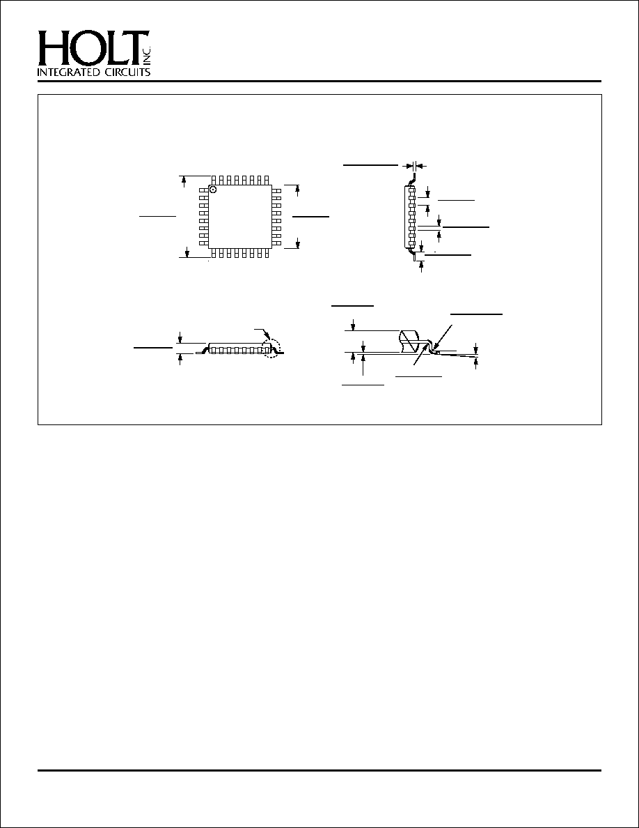
PACKAGE DIMENSIONS
inches (millimeters)
HOLT INTEGRATED CIRCUITS
6
.3543 BSC
(9.00 BSC) SQ.
.063 MAX.
(1.60 MAX.)
.0315 BSC
(0.80 BSC)
.0148 .0030
±
(0.375 ± .075)
.0551 .002
±
(1.4 ± .05)
.0031 R MIN.
(0.08 R MIN.)
.0039 .002
±
(0.10 ± .05)
0∞
7∞
£ Q £
.2755 BSC
(7.00 BSC)
SQ.
See Detail A
Detail A
.0055R .0024
±
(0.14R ± .06)
.0236 .0059
±
(0.60 ± .15)
Package Type: 32PTQS
32 PIN PLASTIC QUAD FLAT PACK (PQFP)
.00057 .00022
±
(0.0145 ± .0055)