
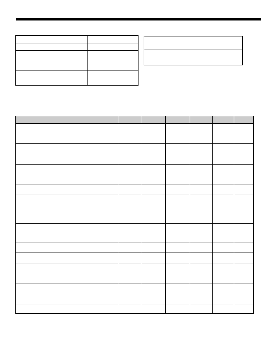
Output A 1
Input A - 2
Input A + 3
V
4
Input B + 5
Input B - 6
Output B 7
I
A, B 8
CC
SET
16 Output D
15 Input D -
14 Input D +
13 V
12 Input C +
11 Input C -
10 Output C
9 I
C, D
EE
SET
HOLT INTEGRATED CIRCUITS
!
!
!
!
!
!
!
Oscillators
Function generators
Active filters
Logic level converters
Voltage reference
Zero crossing detectors
Instrumentation
APPLICATIONS
HI-8573, HI-8574, HI-8575
Quad CMOS Op Amp / Comparator
DESCRIPTION
FEATURES
PIN CONFIGURATION
The HI-8573, HI-8574 and HI-8575 devices are designed
using low power CMOS technology. The operating current
is externally programmable with a resistor to give the
optimum tradeoff between power dissipation and slew
rate. The operational amplifiers are internally
compensated.
All three versions offer a high degree of versatility and are
well suited for both line-powered and battery-powered
systems.
Features include a typical offset voltage of
±5 mV, high input impedance and low current drain.
Either single or dual power supply operation may be
used up to 15V DC. The comparators are CMOS and
TTL compatible. The three devices are direct
replacements for the Motorola/ON-Semiconductor
MC14573, MC14574 and MC14575 respectively.
!
!
!
!
!
!
!
!
!
Single or dual power supply. +3 to 15Vdc
or ±1.5 to ±7.5Vdc
Wide input voltage range
Common mode range 0 to V
-2V single
supply
Adjustable current / slew rate
Typical offset ±5 mV
Internally compensated op amps
High input impedance
CMOS and TTL compatible comparators
Direct replacements for Motorola / On
Semiconductor MC14573, MC14574 and
MC14575
CC
16 Pin Plastic DIP & SOIC packages
February 2003
www.holtic.com
(DS8573 Rev. A)
02/03

HOLT INTEGRATED CIRCUITS
2
HI-8573, HI-8574, HI-8575
PIN DESCRIPTIONS
PROGRAMMING CURRENT
The programming current I
is fixed by an external re-
sistor R
connected between V
and either one or
both of the I
pins (8 and 9). When two external pro-
gramming resistors are used, the set currents for each op
amp pair or comparator are given by:
I
( A)
(V
-V
-1.0)/R
(M )
Pins 8 and 9 may be tied together for use with a single pro-
gramming resistor. The set currents for each op amp or
comparator pair are then given by:
SET
SET
EE
SET
SET
CC
EE
SET
m
W
@
I
( A)
(V
-V
-1.0)/2 R
(M )
If a pair of op amps or comparators are not used, the I
pin for that pair may be tied to V
for minimum power
consumption.
SET
CC
EE
SET
SET
CC
m
W
@
It should be noted that increasing I
for comparators
will decrease propagation delay for that comparator.
For operational amplifiers, the maximum obtainable out-
put voltage (V
) for a given load resistor connected to
V
is given by:
V
= (4 x 10 I
)R - 0.05V
if (4 x 10 I
) R < V
where, R is in K , I
is in A
Typical op amp slew rates are given by:
S
0.05 I
(V/ s).
where, I
is in A
SET
OH
EE
OH
SET
L
SET
L
L
SET
R
SET
SET
-3
-3
CC
W
m
@
m
m
PIN
SYMBOL
FUNCTION
DESCRIPTION
HI-8573
HI-8574
HI-8575
1
Output A
Analog output
Amplifier A
Comparator A
Amplifier A
2
Input A-
Analog input
Amplifier A
Comparator A
Amplifier A
3
Input A+
Analog input
Amplifier A
Comparator A
Amplifier A
4
V
Power
Positive supply voltage
5
Input B+
Analog input
Amplifier B
Comparator B
Amplifier B
6
Input B-
Analog input
Amplifier B
Comparator B
Amplifier B
7
Output B
Analog output
Amplifier B
Comparator B
Amplifier B
8
I
A, B
Analog input
Bias control for A and B
9
I
C, D
Analog input
Bias control for C and D
10
Output C
Analog output
Amplifier C
Comparator C
Comparator C
11
Input C-
Analog input
Amplifier C
Comparator C
Comparator C
12
Input C+
Analog input
Amplifier C
Comparator C
Comparator C
13
V
Power
Negative supply voltage
14
Input D+
Analog input
Amplifier D
Comparator D
Comparator D
15
Input D-
Analog input
Amplifier D
Comparator D
Comparator D
16
Output D
Analog output
Amplifier D
Comparator D
Comparator D
CC
SET
SET
EE
HOLT INTEGRATED CIRCUITS
2
HI-8573, HI-8574, HI-8575
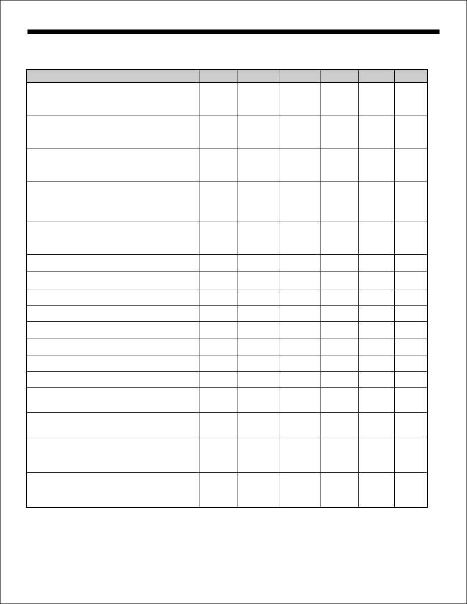
PARAMETER
SYMBOL
V
MIN
TYP
MAX
UNITS
CC
Input common mode voltage range
5
0
3
10
0
8
15
0
13
Output voltage range
(I
= 50
(R = 100 K
connected to V
)
Average temperature coefficient of V
V
20
V/∞C
Input bias current
I
10
1
nA
Input offset current
I
10
200
pA
Open loop voltage gain
(ISET =
A
10
90
dB
Power supply rejection ratio
PSRR
10
70
dB
Common mode rejection ratio
CMRR
10
80
dB
(I
= 200 A)
V
Vdc
5
1.05
4
V
10
1.05
9
Vdc
15
1.05
14
Input offset voltage
V
10
±5
±25
mVdc
/ T
50
Channel separation
10
-100
dB
Slew rate
S
10
2.5
V/ s
Phase margin
M
10
45
Degrees
Supply current, per pair
(R
= 1 M
5
50
I
10
100
A
15
150
Supply current, per pair
R
= 100 K
5
0.5
I
10
1.2
mA
15
1.8
Gain x Bandwidth product
G
10
1.4
MHz
SET
ICR
OR
IO
O
R
SET
CC
SET
CC
BP
m
m
D
m
m
F
m
(
SET
L
EE
IO
I
IB
IO
VOL
A)
A)
)
)
W
D
m
W
W
NOTE:
Stresses above absolute maximum
ratings or outside recommended operating
conditions may cause permanent damage to the
device. These are stress ratings only. Operation
at the limits is not recommended.
Supply voltage (
Input voltage. All inputs
Storage temperature range
-60 to +150 ∞C
Solder Temperature (Leads)
275∞C for 10 sec
Solder Temperature (Body)
220∞C
V
)
-0.5 V to +18 V
-0.5 V to V
+0.5 V
DC input current, per pin
±10 mA
Programming current range
2.0 mA
CC
CC
ABSOLUTE MAXIMUM RATINGS
RECOMMENDED OPERATING CONDITIONS
Supply Voltage
Temperature Range
Industrial Screening.........-40∞C to +85∞C
V
-V
.......................... +3.0 to +15 V
CC
EE
ELECTRICAL CHARACTERISTICS - OPERATIONAL AMPLIFIER
V
= 0 V, T = 25∞C (unless otherwise specified).
EE
A
HOLT INTEGRATED CIRCUITS
3
HOLT INTEGRATED CIRCUITS
4
PARAMETER
SYMBOL
V
MIN
TYP
MAX
UNITS
CC
Input common mode voltage range
(ISET = 200
5
0
3
10
0
8
15
0
13
Output low voltage "0" level
10
0
0.05
15
0
0.05
Average temperature coefficient of V
V
20
V/∞C
Input bias current
I
10
1
nA
Input offset current
I
10
200
pA
Open loop voltage gain
(I
= 50
A
10
m
m
D
m
m
W
m
W
A)
V
V
5
0
0.05
V
V
Output high voltage "1" level
5
4.95
5
V
10
9.95
10
V
15
14.95
15
Output source current
(V
= 2.5 V)
5
-0.24
-0.42
(V
= 4.6 V)
I
5
-0.51
-0.88
mAdc
(V
= 9.5 V)
10
-1.3
-2.25
(V
= 13.5 V)
15
-3.4
-8.8
Output sink current
(V
= 0.4 V)
5
1.25
2.25
(V
= 0.5 V)
I
10
3.25
5.6
mAdc
(V
= 1.5 V)
15
8.5
20
Input offset voltage
(ISET = 50 A)
V
10
±5
±25
mVdc
/ T
A)
96
dB
Power supply rejection ratio
PSRR
10
70
dB
Common mode rejection ratio
CMRR
10
80
dB
Channel separation
10
-100
dB
Output rise and fall time
(C = 50 pF)
tT
10
100
ns
tT
Propagation delay time,
(I
= 50 A, CL = 50 pF)
tD
10
1000
ns
5 mV overdrive
Supply current, per pair
(RSET = 1 M )
5
50
I
10
100
A
15
150
Supply current, per pair
(RSET = 100 K )
5
0.45
I
10
1.0
mA
15
1.5
ICR
OL
OH
OH
OH
OH
OH
OH
OL
OL
OL
OL
IO
O
L
LH
HL
SET
CC
CC
IO
I
IB
IO
SET
VOL
D
m
HI-8573, HI-8574, HI-8575
ELECTRICAL CHARACTERISTICS - COMPARATOR
V
= 0V, T = 25∞C (unless otherwise specified).
EE
A
NOTE: Unused inputs should always be tied to either V
or V
CC
EE
ELECTRICAL CHARACTERISTICS - COMPARATOR
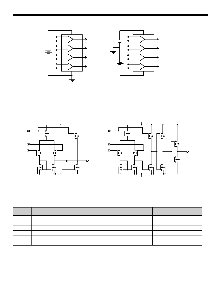
HI-8573PDI
QUAD OP AMP
16 PIN PLASTIC DIP
-40 ∞C TO +85 ∞C
I
NO
SOLDER
HI-8574PDI
QUAD COMPARATOR
16 PIN PLASTIC DIP
-40 ∞C TO +85 ∞C
I
NO
SOLDER
HI-8575PDI
DUAL OP AMP / DUAL COMPARATOR
16 PIN PLASTIC DIP
-40 ∞C TO +85 ∞C
I
NO
SOLDER
HI-8573PSI
QUAD OP AMP
16 PIN SOIC - NB
-40 ∞C TO +85 ∞C
I
NO
SOLDER
HI-8574PSI
QUAD COMPARATOR
16 PIN SOIC - NB
-40 ∞C TO +85 ∞C
I
NO
SOLDER
HI-8575PSI
DUAL OP AMP / DUAL COMPARATOR
16 PIN SOIC - NB
-40 ∞C TO +85 ∞C
I
NO
SOLDER
HOLT INTEGRATED CIRCUITS
5
HI-8573, HI-8574, HI-8575
PACKAGE
DESCRIPTION
TEMPERATURE
RANGE
PART
NUMBER
LEAD
FINISH
ORDERING INFORMATION
FUNCTION
PROCESS
FLOW
BURN
IN
POWER OPTIONS
Single Supply
V
EE
V
CC
3.0 to 15 V
Split Supply
V
EE
V
CC
1.5 to 7.5 V
1.5 to 7.5 V
CIRCUIT DIAGRAMS
INPUT (+)
INPUT (-)
ISET
OUTPUT
INPUT (+)
INPUT (-)
ISET
OUTPUT
V
CC
V
EE
V
CC
V
EE
Operational Amplifier
Comparator
Legend:
NB
- Narrow Body

PACKAGE DIMENSIONS
inches (millimeters)
HOLT INTEGRATED CIRCUITS
6
Package Type:
0∞ to 8∞
Detail A
16-PIN PLASTIC SMALL OUTLINE - NB
(Narrow Body)
.0069 ± .0029
(.175 ± .074)
.033 ± .017
(.838 ± .432)
Package Type: 16HN
.061 ± .007
(1.549 ± .178)
.050 ±.010
(1.270 ±.254)
.050 .010
(1.270 .254)
.0165 ± .0035
(.419 ± ..089)
.3898 ± .0039
(9.901 ± .099)
.0165 ± .0035
(.419 ± ..089)
.236 ±.008
(6.00 ±.20)
.236 .008
(6.00 .20)
.00865 ± .00115
(.220 ± .029)
Detail A
.1535 ± .0035
(3.899 ± .089)
Top View
Package Type:
7∞ TYP.
.777 ±.033
(19.736 ±.838)
.135 ±.015
(3.429 ±.381)
0∞ ~ 15∞
.340 ±.040
(8.636± 1.016)
.019 ±.004
(.483 ±.102)
.055 ±.010
(1.397± .254)
.100 ±.010
(3.540 ±.254)
.130 ±.020
(3.302 ±.508)
.250 ±.010
(6.350 ± .254)
.305 ±.015
(7.747 ±.381)
.160 ±.025
(4.064 ±.635)
16-PIN PLASTIC DIP
16P