HI-8582, HI-8583
ARINC 429 System on a Chip
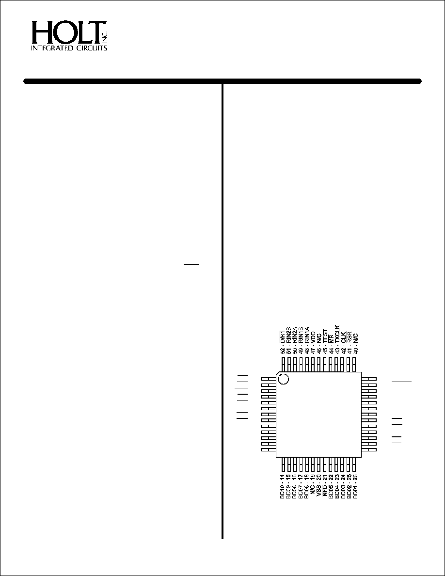
PIN CONFIGURATION
(Top View)
HI-8582PQI
&
HI-8582PQT
39 - N/C
38 -
37 - ENTX
36 - V+
35 - TXBOUT
34 - TXAOUT
33 - V-
32 -
31 -
30 - TX/R
29 -
28 -
27 - BD00
CWSTR
FFT
HFT
PL2
PL1
FF1
HF1
D/R2
FF2
HF2
EN1
EN2
- 1
- 2
- 3
- 4
- 5
SEL - 6
- 7
- 8
BD15 - 9
BD14 - 10
BD13 - 11
BD12 - 12
BD11 - 13
GENERAL DESCRIPTION
The HI-8582 from Holt Integrated Circuits is a silicon gate
CMOS device for interfacing a 16-bit parallel data bus
directly to the ARINC 429 serial bus. The HI-8582 design
offers many enhancements to the industry standard HI-
8282 architecture. The device provides two receivers each
with label recognition, 32 by 32 FIFO, and analog line
receiver. Up to 16 labels may be programmed for each
receiver. The independent transmitter has a 32 by 32 FIFO
and a built-in line driver. The status of all three FIFOs can
be monitored using the external status pins, or by polling
the HI-8582's status register. Other new features include a
programmable option of data or parity in the 32nd bit, and
the ability to unscramble the 32 bit word. Also, versions
are available with different values of input resistance and
output resistance to allow users to more easily add external
lightning protection circuitry. The device can be used at
nonstandard data rates when an option pin,
, is
invoked.
The 16-bit parallel data bus exchanges the 32-bit ARINC
data word in two steps when either loading the transmitter
or interrogating the receivers. The databus, and all control
signals are CMOS and TTL compatible.
The HI-8582 applies the ARINC protocol to the receivers
and transmitter. Timing is based on a 1 Megahertz clock.
Although the line driver shares a common substrate with
the receivers, the design of the physical isolation does not
allow parasitic crosstalk, and thereby achieves the same
isolation as common hybrid layouts.
NFD
APPLICATIONS
!
!
!
Avionics data communication
Serial to parallel conversion
Parallel to serial conversion
FEATURES
!
!
!
!
!
!
!
!
!
!
ARINC specification 429 compatible
Dual receiver and transmitter interface
Programmable label recognition
32 x 32 FIFOs each receiver and transmitter
Status register
Data scramble control
32nd transmit bit can be data or parity
Self test mode
Low power
Industrial & full military temperature ranges
!
!
!
Analog line driver and receivers connect
directly to ARINC bus
On-chip 16 label memory for each receiver
Independent data rate selection for
transmitter and each receiver
HOLT INTEGRATED CIRCUITS
1
(DS8582 Rev. H)
06/01
52 - Pin Plastic Quad Flat Pack (PQFP)
(See page 14 for additional pin configuration)
June 2001

SIGNAL
FUNCTION
DESCRIPTION
VDD
POWER
+5V � %
BD05
I/O
Data Bus
BD04
I/O
Data Bus
BD03
I/O
Data Bus
BD02
I/O
Data Bus
5
RIN1A
INPUT
ARINC receiver 1 positive input
RIN1B
INPUT
ARINC receiver 1 negative input
RIN2A
INPUT
ARINC receiver 2 positive input
RIN2B
INPUT
ARINC receiver 2 negative input
OUTPUT
Receiver 1 data ready flag
OUTPUT
FIFO full Receiver 1
OUTPUT
FIFO Half full, Receiver 1
OUTPUT
Receiver 2 data ready flag
OUTPUT
FIFO full Receiver 2
OUTPUT
FIFO Half full, Receiver 2
SEL
INPUT
Receiver data byte selection (0 = BYTE 1) (1 = BYTE 2)
INPUT
Data Bus control, enables receiver 1 data to outputs
INPUT
Data Bus control, enables receiver 2 data to outputs if
is high
BD15
I/O
Data Bus
BD14
I/O
Data Bus
BD13
I/O
Data Bus
BD12
I/O
Data Bus
BD11
I/O
Data Bus
BD10
I/O
Data Bus
BD09
I/O
Data Bus
BD08
I/O
Data Bus
BD07
I/O
Data Bus
BD06
I/O
Data Bus
GND
POWER
0 V
BD01
I/O
Data Bus
BD00
I/O
Data Bus
INPUT
Latch enable for byte 1 entered from data bus to transmitter FIFO.
INPUT
Latch enable for byte 2 entered from data bus to transmitter FIFO. Must follow
TX/R
OUTPUT
Transmitter ready flag. Goes low when ARINC word loaded into FIFO. Goes high
after transmission and FIFO empty.
OUTPUT
Transmitter FIFO Half Full
OUTPUT
Transmitter FIFO Full
V-
POWER
-9.5V to -12.6V
TXAOUT
OUTPUT
Line driver output - A side
TXBOUT
OUTPUT
Line driver output - B side
V+
POWER
+9.5V to +12.6V
ENTX
INPUT
Enable Transmission
INPUT
Clock for control word register
INPUT
Read Status Register if SEL=0, read Control Register if SEL=1
INPUT
No frequency discrimination if low (pull-up)
CLK
INPUT
Master Clock input
TX CLK
OUTPUT
Transmitter Clock equal to Master Clock (CLK), divided by either 10 or 80.
INPUT
Master Reset, active low
TEST
INPUT
Disable Transmitter output if high (pull-down)
D/R1
FF1
HF1
D/R2
FF2
HF2
EN1
EN2
EN1
PL1
PL2
PL1.
HFT
FFT
CWSTR
RSR
NFD
MR
PIN DESCRIPTIONS
HI-8582, HI-8583
HOLT INTEGRATED CIRCUITS
2

SR
Bit
FUNCTION
STATE
DESCRIPTION
SR0
Data ready
0
Receiver 1 FIFO empty
1
Receiver 1 FIFO contains valid data
Resets to zero when all data has
been read.
pin is the inverse of
this bit
(Receiver 1)
SR1
FIFO half full
0
Receiver 1 FIFO holds less than 16
(Receiver 1)
words
1
Receiver 1 FIFO holds at least 16
words.
pin is the inverse of
this bit.
SR2
FIFO full
0
Receiver 1 FIFO not full
(Receiver 1)
1
Receiver 1 FIFO full. To avoid data
loss, the FIFO must be read within
one ARINC word period.
pin is
the inverse of this bit
SR3
Data ready
0
Receiver 2 FIFO empty
(Receiver 2)
1
Receiver 2 FIFO contains valid data
Resets to zero when all data has
been read.
pin is the inverse of
this bit
SR4
FIFO half full
0
Receiver 2 FIFO holds less than 16
(Receiver 2)
words
1
Receiver 2 FIFO holds at least 16
words.
pin is the inverse of
this bit.
SR5
FIFO full
0
Receiver 2 FIFO not full
(Receiver 2)
1
Receiver 2 FIFO full. To avoid data
loss, the FIFO must be read within
one ARINC word period.
pin is
the inverse of this bit
SR6 Transmitter FIFO
0
Transmitter FIFO not empty
empty
1
Transmitter FIFO empty.
SR7 Transmitter FIFO
0
Transmitter FIFO not full
full
1
Transmitter FIFO full.
pin is the
inverse of this bit.
SR8 Transmitter FIFO
0
Transmitter FIFO contains less than
half full
16 words
1
Transmitter FIFO contains at least
16 words.
pin is the
inverse of this bit.
D/R1
HF1
FF1
D/R2
HF2
FF2
FFT
HFT
CR
Bit
FUNCTION
STATE
DESCRIPTION
CR0
Receiver 1
0
Data rate = CLK/10
select
1
Data rate = CLK/80
Data clock
CR1
Label Memory
0
Normal operation
Read / Write
1
Load 16 labels using
/
Read 16 labels using
/
CR2
Enable Label
0
Disable label recognition
Recognition
(Receiver 1)
1
Enable label recognition
CR3
Enable Label
0
Disable Label Recognition
Recognition
(Receiver 2)
1
Enable Label recognition
CR4
Enable
0
Transmitter 32nd bit is data
32nd bit
as parity
1
Transmitter 32nd bit is parity
CR5
Self Test
0
An internal connection is made
passing TXAOUT and TXBOUT
to the receiver inputs
1
Normal operation
CR6
Receiver 1
0
Receiver 1 decoder disabled
decoder
1
ARINC bits 9 and 10 must match
CR7 and CR8
CR7
-
-
If receiver 1 decoder is enabled,
the ARINC bit 9 must match this bit
CR8
-
-
If receiver 1 decoder is enabled,
the ARINC bit 10 must match this bit
CR9
Receiver 2
0
Receiver 2 decoder disabled
Decoder
1
ARINC bits 9 and 10 must match
CR10 and CR11
CR10
-
-
If receiver 2 decoder is enabled,
the ARINC bit 9 must match this bit
CR11
-
-
If receiver 2 decoder is enabled,
the ARINC bit 10 must match this bit
CR12
Invert
0
Transmitter 32nd bit is Odd parity
Transmitter
parity
1
Transmitter 32nd bit is Even parity
CR13
Transmitter
0
Data rate=CLK/10, O/P slope=1.5us
data clock
select
1
Data rate=CLK/80, O/P slope=10us
CR14
Receiver 2
0
Data rate=CLK/10
data clock
select
1
Data rate=CLK/80
CR15
Data
0
Scramble ARINC data
format
1
Unscramble ARINC data
PL1 PL2
EN1 EN2
FUNCTIONAL DESCRIPTION
CONTROL WORD REGISTER
The HI-8582 contains a 16-bit control register which is used to
configure the device. The control register bits CR0 - CR15 are
loaded from BD00 - BD15 when
is pulsed low. The control
register contents are output on the databus when SEL=1 and
is pulsed low. Each bit of the control register has the following
function:
CWSTR
RSR
STATUS REGISTER
The HI-8582 contains a 9-bit status
register which can be
interrogated to determine the status of the ARINC receivers, data
FIFOs and transmitter. The contents of the status register are output
on BD00 - BD08 when the
pin is taken low and SEL = 0. Unused
bits are output as zeros. The following table defines the status
register bits.
RSR
HI-8582, HI-8583
HOLT INTEGRATED CIRCUITS
3

FIGURE 1. ARINC RECEIVER INPUT
BYTE 2
DATA
BD BD BD BD BD BD BD BD BD BD BD BD BD BD BD BD
BUS
15 14 13 12 11 10 09 08 07 06 05 04 03 02 01 00
ARINC
29 28 27 26 25 24 23 22 21 20 19 18 17 16 15 14
BIT
CR15=0
ARINC
32 31 30 29 28 27 26 25 24 23 22 21 20 19 18 17
CR15=1
The HI-8582 guarantees recognition of these levels with a common
mode Voltage with respect to GND less than �5V for the worst case
condition (4.75V supply and 13V signal level).
The tolerances in the design guarantee detection of the above
levels, so the actual acceptance ranges are slightly larger. If the
ARINC signal is out of the actual acceptance ranges, including the
nulls, the chip rejects the data.
RECEIVER LOGIC OPERATION
BIT TIMING
BIT RATE
PULSE RISE TIME
PULSE FALL TIME
PULSE WIDTH
Figure 2 shows a block diagram of the logic section of each receiver.
The ARINC 429 specification contains the following timing specifi-
cation for the received data:
100K BPS � 1% 12K -14.5K BPS
1.5 � 0.5 �sec
10 � 5 �sec
1.5 � 0.5 �sec
10 � 5 �sec
5 �sec � 5%
34.5 to 41.7 �sec
If the
pin is high, the HI-8582 accepts signals that meet these
specifications and rejects outside the tolerances. The way the logic
operation achieves this is described below:
HIGH SPEED
LOW SPEED
NFD
3. Each data bit must follow its predecessor by not less than 8
samples and no more than 12 samples. In this manner the bit
rate is checked. With exactly 1MHz input clock frequency, the
acceptable data bit rates are as follows:
83K BPS
10.4K BPS
125K BPS
15.6K BPS
4. The Word Gap timer samples the Null shift register every 10
input clocks (80 for low speed) after the last data bit of a valid
reception. If the Null is present, the Word Gap counter is
incremented. A count of 3 will enable the next reception.
HIGH SPEED
LOW SPEED
DATA BIT RATE MIN
DATA BIT RATE MAX
If
is held low, frequency discrimination is disabled and any
data stream totaling 32 bits is accepted even with gaps between
bits. The protocol still requires a word gap as defined in 4. above.
NFD
FUNCTIONAL DESCRIPTION (cont.)
THE RECEIVERS
ARINC BUS INTERFACE
Figure 1 shows the input circuit for each receiver. The ARINC 429
specification requires the following detection levels:
ONE
+6.5 Volts to +13 Volts
NULL
+2.5 Volts to -2.5 Volts
ZERO
-6.5 Volts to -13 Volts
STATE
DIFFERENTIAL VOLTAGE
1. Key to the performance of the timing checking logic is an ac-
curate 1MHz clock source. Less than 0.1% error is recom-
mended.
2. The sampling shift registers are 10 bits long and must show
three consecutive Ones, Zeros or Nulls to be considered valid
data. Additionally, for data bits, the One or Zero in the upper
bits of the sampling shift registers must be followed by a Null in
the lower bits within the data bit time. For a Null in the word gap,
three consecutive Nulls must be found in both the upper and
lower bits of the sampling shift register. In this manner the mini-
mum pulse width is guaranteed.
ARINC 429 DATA FORMAT
Control register bit CR15 is used to control how individual bits in the
received or transmitted ARINC word are mapped to the HI-8582 data
bus during data read or write operations. The following table
describes this mapping:
DATA
BD BD BD BD BD BD BD BD BD BD BD BD BD BD BD BD
BUS
15 14 13 12 11 10 09 08 07 06 05 04 03 02 01 00
ARINC
13 12 11 10
9
31 30 32
1
2
3
4
5
6
7
8
BIT
CR15=0
BYTE 1
ARINC
16 15 14 13 12 11 10
9
8
7
6
5
4
3
2
1
BIT
CR15=1
HI-8582, HI-8583
HOLT INTEGRATED CIRCUITS
4

FIFO
LOAD
CONTROL
SEL
EN
CONTROL
BIT
/
R/W
CONTROL
32 TO 16 DRIVER
32 BIT SHIFT REGISTER
TO PINS
CONTROLBITS
CR0, CR14
CLOCK
OPTION
CLOCK
CLK
BIT
COUNTER
AND
END OF
SEQUENCE
PARITY
CHECK
32ND
BIT
DATA
BIT CLOCK
WORD GAP
WORD GAP
TIMER
BIT CLOCK
END
START
SEQUENCE
CONTROL
ERROR
CLOCK
ERROR
DETECTION
SHIFT REGISTER
SHIFT REGISTER
NULL
ZEROS
SHIFT REGISTER
ONES
EOS
FIGURE 2.
RECEIVER BLOCK DIAGRAM
LABEL /
DECODE
COMPARE
16 x 8
LABEL
MEMORY
32 X 32
FIFO
D/R
FF
MUX
CONTRO
L
CONTROL
BITS
HF
FUNCTIONAL DESCRIPTION (cont.)
0
X
0
X
Load FIFO
1
No
0
X
Ignore data
1
Yes
0
X
Load FIFO
0
X
1
No
Ignore data
0
X
1
Yes
Load FIFO
1
Yes
1
No
Ignore data
1
No
1
Yes
Ignore data
1
No
1
No
Ignore data
1
Yes
1
Yes
Load FIFO
CR2(3) ARINC word CR6(9) ARINC word
FIFO
matches
bits 9,10
label
match
CR7,8 (10,11)
RECEIVER PARITY
The receiver parity circuit counts ones received, including the
parity bit. If the result is odd, then "0" will appear in the 32nd bit.
RETRIEVING DATA
Once 32 valid bits are recognized, the receiver logic generates an
End of Sequence (EOS). Depending upon the state of control
register bits CR2-CR11, the received ARINC 32-bit word is then
checked for correct decoding and label matching before being
loaded into the 32 x 32 receive FIFO. ARINC words which do not
meet the necessary 9th and 10th ARINC bit or label matching are
ignored and are not loaded into the receive FIFO. The following
table describes this operation.
HI-8582, HI-8583
HOLT INTEGRATED CIRCUITS
5