
HI-8585, HI-8586
ARINC 429 LINE DRIVER
DESCRIPTION
!
Direct ARINC 429 line driver interface
in a small package
On-chip zener to set output levels
On-chip line driver slope control and
selection by logic input
Low current 12 to 15 volt supplies
CMOS / TTL logic pins
Plastic and ceramic package options -
surface mount and DIP
!
!
!
!
!
!
!
Thermally enhanced SOIC packages
Mil processing available
FEATURES
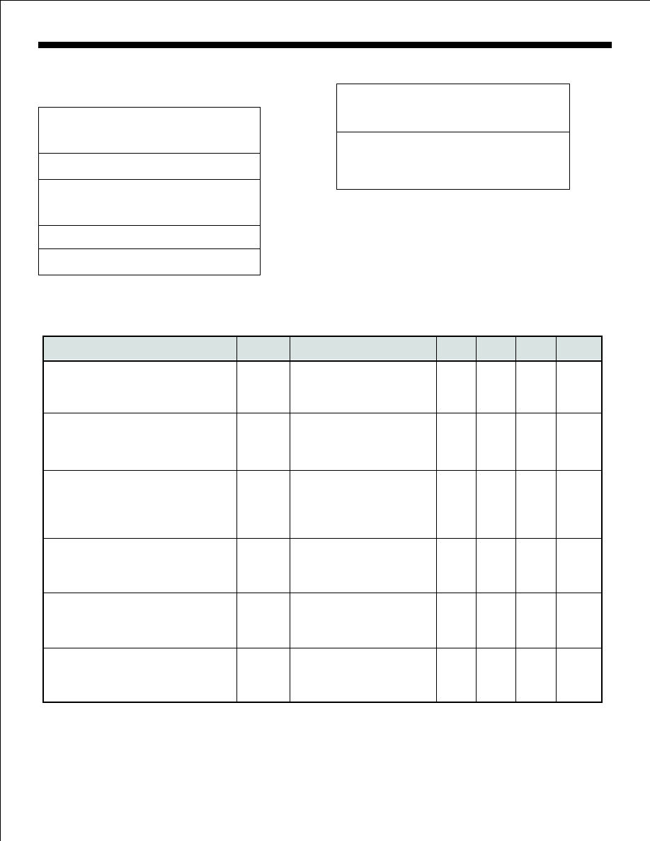
PIN CONFIGURATION
SLP1.5
TX0IN
TX1IN
GND
V-
TXAOUT
TXBOUT
V+
SUPPLY VOLTAGES
FUNCTION TABLE
The HI-8585 and HI-8586 are CMOS integrated circuits
designed to directly drive the ARINC 429 bus in an 8-pin
package. Two logic inputs control a differential voltage
between the output pins producing a +10 volt One, a
-10 volt Zero, and a 0 volt Null.
The CMOS/TTL control inputs are translated to ARINC
specified amplitudes using on board zeners. A logic input
is provided to control the slope of the differential output
signal. Timing is set by on-chip resistor and capacitor and
tested to be within ARINC requirements.
The HI-8585 has 37.5 ohms in series with each line driver
output. The HI-8586 provides the option to bypass most of
the output resistance so that external series protection
circuits can add their resistances.
The HI-8585 or the HI-8586 along with the HI-8588 line
receiver offer the smallest options available to get on and
off the ARINC bus.
PIN DESCRIPTION TABLE
V+ =
12V to 15V
V- =
-12V to -15V
1
2
3
4
5
6
7
8
February 2003
www.holtic.com
02/03
(DS8585 Rev. F)
1
2
3
4
5
6
7
8
PIN
SLP 1.5
TX0IN
TX1IN
GND
V-
TXAOUT
TXBOUT
V+
SYMBOL
LOGIC INPUT
LOGIC INPUT
LOGIC INPUT
POWER
POWER
OUTPUT
OUTPUT
POWER
FUNCTION
CMOS OR TTL, V+ IS OK
CMOS OR TTL
CMOS OR TTL
GROUND
-12 TO -15 VOLTS
LINE DRIVER TERMINAL A
LINE DRIVER TERMINAL B
+12 TO +15 VOLTS
DESCRIPTION
0
0
0
1
1
1
TX1IN TX0IN SLP1.5
TXAOUT
TXBOUT
SLOPE
0
1
1
0
0
1
X
0
1
0
1
X
0V
-5V
-5V
5V
5V
0V
0V
5V
5V
-5V
-5V
0V
N/A
10 s
m
1.5 s
m
10 s
m
1.5 s
m
N/A
HOLT INTEGRATED CIRCUITS

Figure 2 shows a possible application
of the HI-8585/86 interfacing an ARINC
transmit channel from the HI-6010.
HI-8585, HI-8586
FUNCTIONAL DESCRIPTION
TXAOUT
CURRENT
CONTROL
-5V
5V
ONE
NULL
ZERO
CONTROL
LOGIC
TXBOUT
CURRENT
CONTROL
-5V
5V
SLP1.5
ESD
PROTECTION
AND
VOLTAGE
TRANSLATION
TX0IN
TX1IN
FIGURE 1 - LINE DRIVER BLOCK DIAGRAM
HI-8585 = 37.5 OHMS
HI-8586 = < 5 OHMS
HI-8585 = 37.5 OHMS
HI-8586 = < 5 OHMS
ONE
NULL
ZERO
CONTROL
LOGIC
"A" SIDE
"B" SIDE
GND
8
TXBOUT
TXAOUT
TX1IN
TX0IN
ARINC
Channel
RINB
RINA
TESTA
TESTB
{
HARDWIRED
OR
DRIVEN FROM LOGIC
ROUTB
ROUTA
5V
VCC
V-
-15V
SLP1.5
TXD0
TXD1
RXD0
RXD1
HI-6010
8 BIT BUS
ARINC
Channel
1
2
8
6
7
4
3
4
5
6
7
2
3
HI-8588
FIGURE 2 - APPLICATION DIAGRAM
APPLICATION INFORMATION
15V
V+
1
5
HI-8585
Figure 1 is a block diagram of the line driver. The +5V and
-5V levels are generated internally using on-chip zeners.
Currents for slope control are set by zener voltages across
on-chip resistors.
The TX0IN and TX1IN inputs receive logic signals from a
control transmitter chip such as the HI-6010, HI-3282 or
HI-8282. TXAOUT and TXBOUT hold each side of the
ARINC bus at Ground until one of the inputs becomes a
One. If for example TX1IN goes high, a charging path is
enabled to 5V on an "A" side internal capacitor while the
"B" side is enabled to -5V. The charging current is se-
lected by the SLP1.5 pin. If the SLP1.5 pin is high, the
capacitor is nominally charged from 10% to 90% in 1.5µs.
If SLP1.5 is low, the rise and fall times are 10µs.
A unity gain buffer receives the internally generated slopes
and differentially drives the ARINC line. Current is limited
by the series output resistors at each pin. There are no
fuses at the outputs of the HI-8585 as exists on the HI-
8382.
The HI-8585 has 37.5 ohms in series with each output.
The HI-8586 has less than 5 ohms in series. The HI-8586
is for applications where external series resistance is re-
quired, typically for lightning protection devices.
Both the HI-8585 and HI-8586 are built using high-speed
CMOS technology. Care should be taken to ensure the
V+ and V- supplies are locally decoupled and that the
input waveforms are free from negative voltage spikes
which may upset the chip's internal slope control circuitry.
HOLT INTEGRATED CIRCUITS
2
NOTE: Stresses above absolute maximum
ratings or outside recommended operating
conditions may cause permanent damage to
the device.
These are stress ratings only.
Operation at the limits is not recommended.
HI-8585, HI-8586
Voltages referenced to Ground
Supply voltages
V+....................................................20V
V-....................................................-20V
DC current per input pin................ +10mA
Power dissipation at 25∞C
plastic DIL............1.0W, derate 10mW/∞C
ceramic DIL..........0.5W, derate 7mW/∞C
Solder Temperature ........275∞C for 10 sec
Storage Temperature........-65∞C to +150∞C
ABSOLUTE MAXIMUM RATINGS
RECOMMENDED OPERATING CONDITIONS
Supply Voltages
V+....................+12V ± 5% or +15V ±10%
V-..................... -12V ± 5% or -15V ±10%
Temperature Range
Industrial Screening.........-40∞C to +85∞C
Hi-Temp Screening........-55∞C to +125∞C
Military Screening..........-55∞C to +125∞C
DC ELECTRICAL CHARACTERISTICS
V+ = +12V to +15V, V- = -12V to -15V, T = Operating Temperature Range (unless otherwise stated)
A
PARAMETERS
SYMBOL
TEST CONDITIONS
MIN
TYP
MAX
UNITS
Input voltage (TX1IN, TX0IN, SLP1.5)
high
V
2.1
-
V+
volts
low
V
-
-
0.5
volts
Input current (TX1IN, TX0IN, SLP1.5)
source
I
V
= 0V
-
-
0.1
A
sink
I
= 5V
-
-
0.1
A
ARINC output voltage (Differential)
zero
V
no load
-11.00
-10.00
-9.00
volts
null
V
no load
-0.50
0
0.50
volts
V+
I
-
6.0
14.0
mA
V-
I
-14.0
-6.0
-
mA
ARINC output impedence
Z
HI-8585
-
37.5
-
ohms
HI-8586
-
-
5
ohms
IH
IL
IH
IN
IL
DIFF0
DIFFN
DD
EE
OUT
m
m
V
one
V
no load; TXAOUT - TXBOUT
9.00
10.00
11.00
volts
; TXAOUT - TXBOUT
; TXAOUT - TXBOUT
ARINC output voltage (Ref. to GND)
one or zero
V
no load & magnitude at pin
4.50
5.00
5.50
volts
null
V
no load
-0.25
0
0.25
volts
Operating supply current
IN
DIFF1
DOUT
NOUT
SLP1.5 = V+
TX1IN & TX0IN = 0V: no load
IN & TX1IN = 0V: no load
TX0
HOLT INTEGRATED CIRCUITS
3

V+ = 15.0V, V- = -15V, T = Operating Temperature Range (unless otherwise stated)
A
defined in Figure 3, no load
pin 1 = logic 1
Input capacitance (1)
HI-8585, HI-8586
AC ELECTRICAL CHARACTERISTICS
PARAMETERS
SYMBOL TEST CONDITIONS
MIN
TYP
MAX
UNITS
Line Driver propagation delay
Output high to low
Output low to high
Line Driver transition times
Output high to low
Output low to high
t phlx
plhx
t
t fx
rx
t
-
-
1.0
1.0
2.0
2.0
500
500
1.5
1.5
ns
ns
m
s
m
s
logic
CIN
-
-
10
pF
pin 1 = logic 1
-
-
Notes:
1. Guaranteed but not tested
FIGURE 3 - LINE DRIVER TIMING
0V
10V
-10V
5V
0V
5V
0V
t rx
t
10%
90%
t
t
10%
90%
t rx
t
phlx
t
phlx
t
plhx
t
10%
plhx
t
pin 3
pin 2
t fx
t
fx
V
pin 6 - pin 7
DIFF
SLP 1.5 = V+
HOLT INTEGRATED CIRCUITS
4

HI-8585, HI-8586
Notes:
1. All data taken in still air on devices soldered to single layer copper PCB (3" X 4.5" X .062").
2. At 100% duty cycle, 15V power supplies. For 12V power supplies multiply all tabulated values by 0.8.
3. Low Speed: Data Rate = 12.5 Kbps, Load: R = 400 Ohms, C = 30 nF.
4. High Speed: Data Rate = 100 Kbps, Load: R = 400 Ohms, C = 10 nF. Data not presented for C = 30 nF
as this is considered unrealistic for high speed operation.
5. 8 Lead Plastic ESOIC (Thermally enhanced SOIC with built in heat sink). Heat sink not soldered to the PCB.
6. 8 Lead Plastic ESOIC (Thermally enhanced SOIC with built in heat sink). Heat sink soldered to the PCB.
7. Similar results would be obtained with TXAOUT shorted to TXBOUT.
8. For applications requiring survival with continuous short circuit, operation above Tj = 175∞C is not recommended.
9. Data will vary depending on air flow and the method of heat sinking employed.
PACKAGE THERMAL CHARACTERISTICS
SUPPLY CURRENT (mA)
2
JUNCTION TEMP, Tj (∞C)
Ta = 25
o
C
Ta = 85
o
C
Ta=125
o
C
Ta = 25
o
C
Ta = 85
o
C
Ta=125
o
C
Low Speed
3
16.8
17.2
16.9
58
116
157
High Speed
4
27.3
26.7
25.9
75
132
169
Low Speed
17.4
17.5
16.9
68
126
166
High Speed
27.6
27.1
25.9
97
147
186
Low Speed
17.1
17.2
16.7
52
110
151
High Speed
27.3
27.1
26.2
57
112
157
SUPPLY CURRENT (mA)
2
JUNCTION TEMP, Tj (∞C)
Ta = 25
o
C
Ta = 85
o
C
Ta=125
o
C
Ta = 25
o
C
Ta = 85
o
C
Ta=125
o
C
Low Speed
3
53.6
50.7
52.2
131
181
217
High Speed
4
46.9
38.7
42.5
135
181
219
Low Speed
46.4
47.6
68.1
167
191
221
High Speed
42.1
43.8
67.1
177
212
223
Low Speed
48.5
45.6
46.1
112
161
186
High Speed
46.8
41.1
40.5
116
168
197
8 Lead Plastic ESOIC
5
8 Lead Plastic ESOIC
6
ARINC 429
DATA RATE
ARINC 429
DATA RATE
PACKAGE STYLE
1
8 Lead Plastic DIP
8 Lead Plastic DIP
8 Lead Plastic ESOIC
5
8 Lead Plastic ESOIC
6
PACKAGE STYLE
1
MAXIMUM ARINC LOAD
9
TXAOUT and TXBOUT Shorted to Ground
7, 8, 9
HEAT SINK - ESOIC PACKAGES
An 8-pin thermally enhanced SOIC package is used for the
HI-8585/HI-8586 products. The ESOIC package includes
a metal heat sink located on the bottom surface of the
device. This heat sink should be soldered down to the
printed circuit board for optimum thermal dissipation. The
heat sink is electrically isolated from the chip and can be
soldered to any ground or power plane. However, since
the chip's substrate is at V+, connecting the heat sink to
this power plane is recommended to avoid coupling noise
into the circuit.
HOLT INTEGRATED CIRCUITS
5

HI-8585, HI-8586
ORDERING INFORMATION
Legend:
NB
- Narrow Body
ESOIC - Thermally Enhanced Small Outline Package (SOIC w/built-in heat sink)
PART
PACKAGE
TEMPERATURE
FLOW
BURN
LEAD
NUMBER
DESCRIPTION
RANGE
IN
FINISH
HI-8585PDI
8 PIN PLASTIC DIP
-40∞C T0 +85∞C
I
NO
SOLDER
HI-8585PDT
8 PIN PLASTIC DIP
-55∞C T0 +125∞C
T
NO
SOLDER
HI-8585PDM
8 PIN PLASTIC DIP
-55∞C T0 +125∞C
M
YES
SOLDER
HI-8585PSI
8 PIN PLASTIC ESOIC - NB
-40∞C T0 +85∞C
I
NO
SOLDER
HI-8585PST
8 PIN PLASTIC ESOIC - NB
-55∞C T0 +125∞C
T
NO
SOLDER
HI-8585PSM
8 PIN PLASTIC ESOIC - NB
-55∞C T0 +125∞C
M
YES
SOLDER
HI-8585CRI
8 PIN CERDIP
-40∞C T0 +85∞C
I
NO
SOLDER
HI-8585CRT
8 PIN CERDIP
-55∞C T0 +125∞C
T
NO
SOLDER
HI-8585CRM
8 PIN CERDIP
-55∞C T0 +125∞C
M
YES
SOLDER
HI-8586PDI
8 PIN PLASTIC DIP
-40∞C T0 +85∞C
I
NO
SOLDER
HI-8586PDT
8 PIN PLASTIC DIP
-55∞C T0 +125∞C
T
NO
SOLDER
HI-8586PDM
8 PIN PLASTIC DIP
-55∞C T0 +125∞C
M
YES
SOLDER
HI-8586PSI
8 PIN PLASTIC ESOIC - NB
-40∞C T0 +85∞C
I
NO
SOLDER
HI-8586PST
8 PIN PLASTIC ESOIC - NB
-55∞C T0 +125∞C
T
NO
SOLDER
HI-8586PSM
8 PIN PLASTIC ESOIC - NB
-55∞C T0 +125∞C
M
YES
SOLDER
HI-8586CRI
8 PIN CERDIP
-40∞C T0 +85∞C
I
NO
SOLDER
HI-8586CRT
8 PIN CERDIP
-55∞C T0 +125∞C
T
NO
SOLDER
HI-8586CRM
8 PIN CERDIP
-55∞C T0 +125∞C
M
YES
SOLDER
HOLT INTEGRATED CIRCUITS
6

HI-8585 / HI-8586 PACKAGE DIMENSIONS
inches (millimeters)
HOLT INTEGRATED CIRCUITS
7
8-PIN PLASTIC DIP
Package Type: 8P
.385 ± .015
(4.699 ± .381)
7∞ TYP.
.025 ± .010
(.635
.254)
±
.335 ± .035
(8.509 ± .889)
.250
.010
±
(6.350 ± .254)
.100 ± .010
(3.540 ± .254)
.135 ± .015
(3.429 ± .381)
.055 ± .010
(1.397 ± .254)
.1375 ± .0125
(3.493 ± .318)
.019 ± .002
(.483 ± .102)
.0115 ± .0035
(.292 ± .089)
.300 ± .010
(7.620 ± .254)
D
A
ETAIL
8-PIN PLASTIC SMALL OUTLINE (ESOIC) - NB
(Narrow Body, Thermally Enhanced)
.033 ± .017
(.8382 ± .4318)
.050 ± .010
(1.27 ± .254)
Package Type:
0∞ to 8∞
8HNE
P 1
IN
D
A
ETAIL
Top View
Bottom View
.1535 ± .0035
(3.90 ± .09)
.1935 ± .0035
(4.915 ± .085)
.236 ± .008
(5.994 ± .203)
.0085 ± .0015
(.2159 ± .0381)
.0165 ± .0035
(.4191 ± .0889)
.140 ± .010
(3.556 ± .254)
.100 ± .010
(2.540 ± .254)
.0025 ± .0015
(.0635 ± .0381)
.055 ± .005
(1.397 ± .127)
Electrically isolated metal
heat sink on bottom of
package
(Connect to any ground or
power plane for optimum
thermal dissipation)
HI-8585 / HI-8586 PACKAGE DIMENSIONS
inches (millimeters)
HOLT INTEGRATED CIRCUITS
8
8-PIN CERDIP
Package Type: 8D
.380 ± .004
(9.652 ± .102)
.005 MIN.
(.127 MIN.)
.314 ± .003
(7.976 ± .076)
.200 MAX.
(5.080 MAX.)
.248 ± .003
(6.299 ± .076)
.039 ± .006
(.991 ± .154)
.163 ± .037
(4.140 ± .940)
.018 ± .006
(.457 ± .152)
.056 ± .006
(1.422 ± .152)
.015 MIN.
(.381 MIN.)
.350 ± .030
(8.890 ± .762)
.010 ± .006
(.254 ± .152)
Base Plane
Seating Plane
.100 ± .008
(2.540 ± .203)