 | –≠–Ľ–Ķ–ļ—ā—Ä–ĺ–Ĺ–Ĺ—č–Ļ –ļ–ĺ–ľ–Ņ–ĺ–Ĺ–Ķ–Ĺ—ā: HI-8788 | –°–ļ–į—á–į—ā—Ć:  PDF PDF  ZIP ZIP |

HI-8787, HI-8788
DESCRIPTION
FEATURES
PIN CONFIGURATION
The HI-8787 and HI-8788 are system components for
interfacing 16 bit parallel data to an ARINC 429 bus. They
combine logic and line driver on one chip. The HI-8787 has
an output resistance of 37.5 ohms, and the HI-8788 has
output resistance of 10 ohms to facilitate external lightning
protection circuitry.
The technology is analog/digital
CMOS.
Both products offer high speed data bus transactions into a
buffer register.
After loading 2 16-bit words, data is
automatically transferred and transmitted. The data rate is
equal to the clock rate. Parity can be enabled in the 32nd
bit. Reset is used to initialize the logic upon startup. Word
gaps are automatically sent.
The part requires +/- 10 volt supplies in addition to a 5 volt
supply.
Automatically converts 16 bit parallel data
to ARINC 429 or 561 data
High speed data bus interface
On-chip line driver
Available in small TQFP package
Military processing options
l
l
l
l
l
32-Pin Plastic TQFP package
January 2001
(DS8787 Rev. B)
01/01
24 - TXBOUT
23 - TXAOUT
22 - V-
21 - PARITY ENB
20 - XMT RDY
19 - XMIT CLK
18 -
17 -
RESET
WRITE
D4 - 1
N/C - 2
D5 - 3
D6 - 4
D7 - 5
D8 - 6
D9 - 7
D10 - 8
HI-8787PQI
HI-8787PQT
HI-8788PQI
&
HI-8788PQT
HOLT INTEGRATED CIRCUITS
1
HI-8787, HI-8788
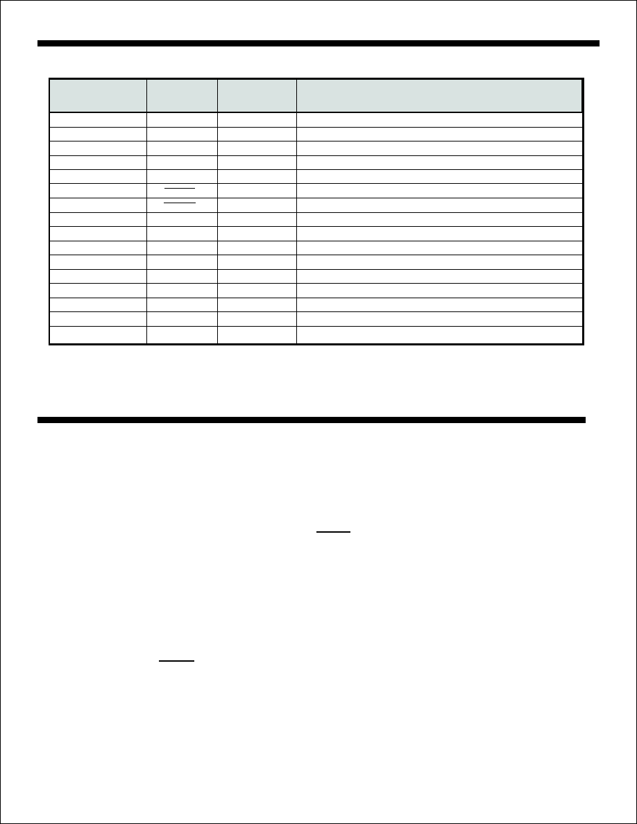
PIN DESCRIPTIONS
FUNCTIONAL DESCRIPTION
PIN
SYMBOL
FUNCTION
DESCRIPTION
28
561 SYNC
digital output
ARINC 561 Sync signal
1, 3-10,13-15, 29-32
Dn
digital inputs
Parallel 16 bit bus input
11
GND
power supply
Ground
12
A0
digital input
Load address, A0=0 for 1st data load, A0=1 for 2nd data load
16
SLP1.5
digital input
Selects the slope of the line driver. High=1.5us
17
digital input
Write strobe. Loads data on rising edge.
18
digital input
Registers and sequencing logic initialized when low
19
XMIT CLK
digital input
Clock input for the transmitter
20
XMT RDY
digital output
Goes high if the buffer register is empty
21
PARITY ENB
digital input
When high the 32nd bit output is odd parity
22
V-
power supply
-10 volt rail
23
TXAOUT
analog output
Line driver output - A side
24
TXBOUT
analog output
Line driver output - B side
25
561 DATA
digital output
Serial output for ARINC 561 data
26
V+
power supply
+10 volt rail
27
VCC
power supply
+5 volt rail, "one" level out of line driver, inverted for "zero"
WRITE
RESET
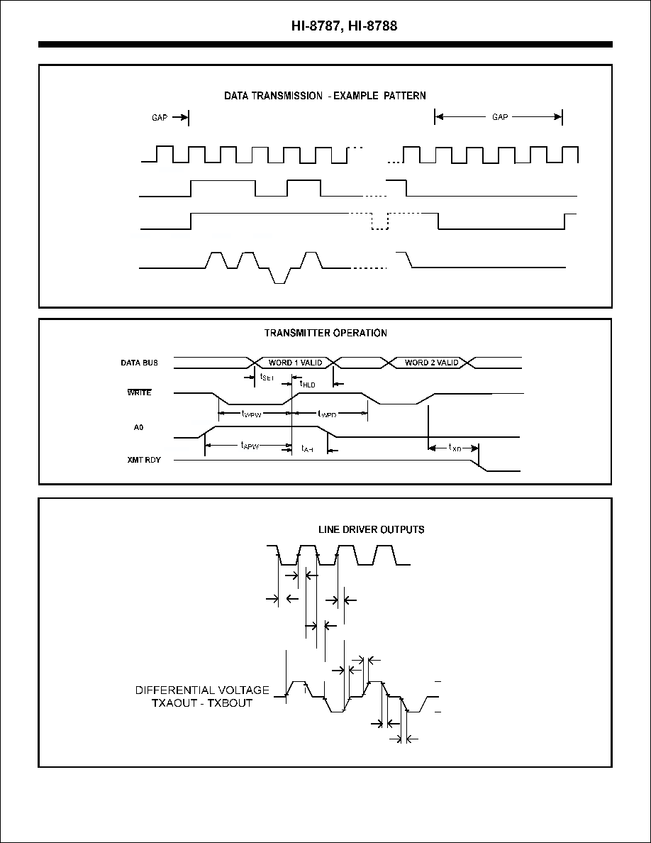
The HI-8787 is a parallel to serial converter, which when
loaded with two 16 bit parallel words, outputs the data as a
32 bit serial word. Timing circuitry inserts a 4 bit gap at the
end of each 32 bit word. An input buffer register allows load
operations to take place while the previously loaded word
is being transmitted.
If the PARITY ENB pin is high, the 32nd bit will be a parity
bit, inserted so as to make the 32 bit word have odd parity. If
the PARITY ENB pin is low, the 32nd bit will be the D15 bit
of the 2nd word loaded.
Outputs are provided for both ARINC 429 (TXAOUT and
TXBOUT pins), and ARINC 561 (561 DATA and 561 SYNC
pins) type data.
A low signal applied to the
pin resets the HI-8787's
internal logic so that spurious transmission does not take
place during power-up. The registers are cleared so that a
continuous gap will be transmitted until the first word is
loaded into the transmitter.
The XMIT CLK frequency is the same as the data rate.
RESET
Input data can be loaded when the XMT RDY signal is
high, which indicates the input buffer register is empty. The
first 16 bit word is loaded with the A0 input high. The sec-
ond word is loaded with A0 in the low state. Each data word
is loaded into the input buffer register by a low pulse on the
input. (See figure 1). After the second word has
been loaded, the XMT RDY output goes low. The contents
of the input buffer register are transferred to the output reg-
ister during the fourth bit period of the gap. If the fourth gap
bit period of the previous word has already been transmit-
ted, the contents of the input buffer register will be trans-
ferred to the output shift register during the first bit period af-
ter the second data load, and the XMT RDY output goes
high.
After the output shift register is loaded, the data is shifted
out to the output logic in the order shown in figure 2.
WRITE
The 561 SYNC output pulses low when the XMIT CLK is
low during the 8th bit of the ARINC transmission.
HOLT INTEGRATED CIRCUITS
2
HOLT INTEGRATED CIRCUITS
2

A0
Load
Data Bus
ARINC Bits
1
Word 1
D0 - D15
ARINC 1 - ARINC 16
0
Word 2
D0 - D15
ARINC 17 - ARINC 32
Figure 2. Order of transmitted data
Figure 1. Block Diagram
DATA
BUS
16 to 32 bit
mux
32 bit
buffer
register
32 bit
shift
register
WRITE
A0
16
32
32
status &
control
logic
XMT RDY
XMIT CLK
word gap
counter
bit
counter
output
logic
line
driver
PARITY ENB
561 DATA
561 SYNC
TXBOUT
TXAOUT
SLP1.5
FUNCTIONAL DESCRIPTION (Cont.)
The HI-8787 and HI-8788 have an on-chip line driver de-
signed to directly drive the ARINC 429 bus. The two ARINC
outputs (TXAOUT and TXBOUT) provide a differential volt-
age to produce a +10 volt One, a -10 volt Zero, and a 0 volt
Null. The slope of the ARINC outputs is controlled by the
SLP1.5 pin. If SLP1.5 is high, the output rise and fall time is
nominally 1.5 s. .If SLP1.5 is set low, the rise and fall times
are 10 s.
The HI-8787 has 37.5 ohms in series with each line driver
output. The HI-8788 has 10.0 ohms in series. The HI-8788
is for applications where external series resistance is
needed, typically for lightning protection devices.
Ķ
Ķ
HOLT INTEGRATED CIRCUITS
3
XMIT CLK
35
36
1
2
3
4
5
31
32
33
34
35
36
561 DATA
561 SYNC
LOW DURING CLK 8
ARINC 429 DATA
(TXAOUT-TXBOUT)
phlx
t
phlx
t
plhx
t
plhx
t
0V
10V
-10V
rx
t
t fx
t
10%
90%
t
t
10%
90%
t rx
t
10%
fx
XMT CLK
HOLT INTEGRATED CIRCUITS
4

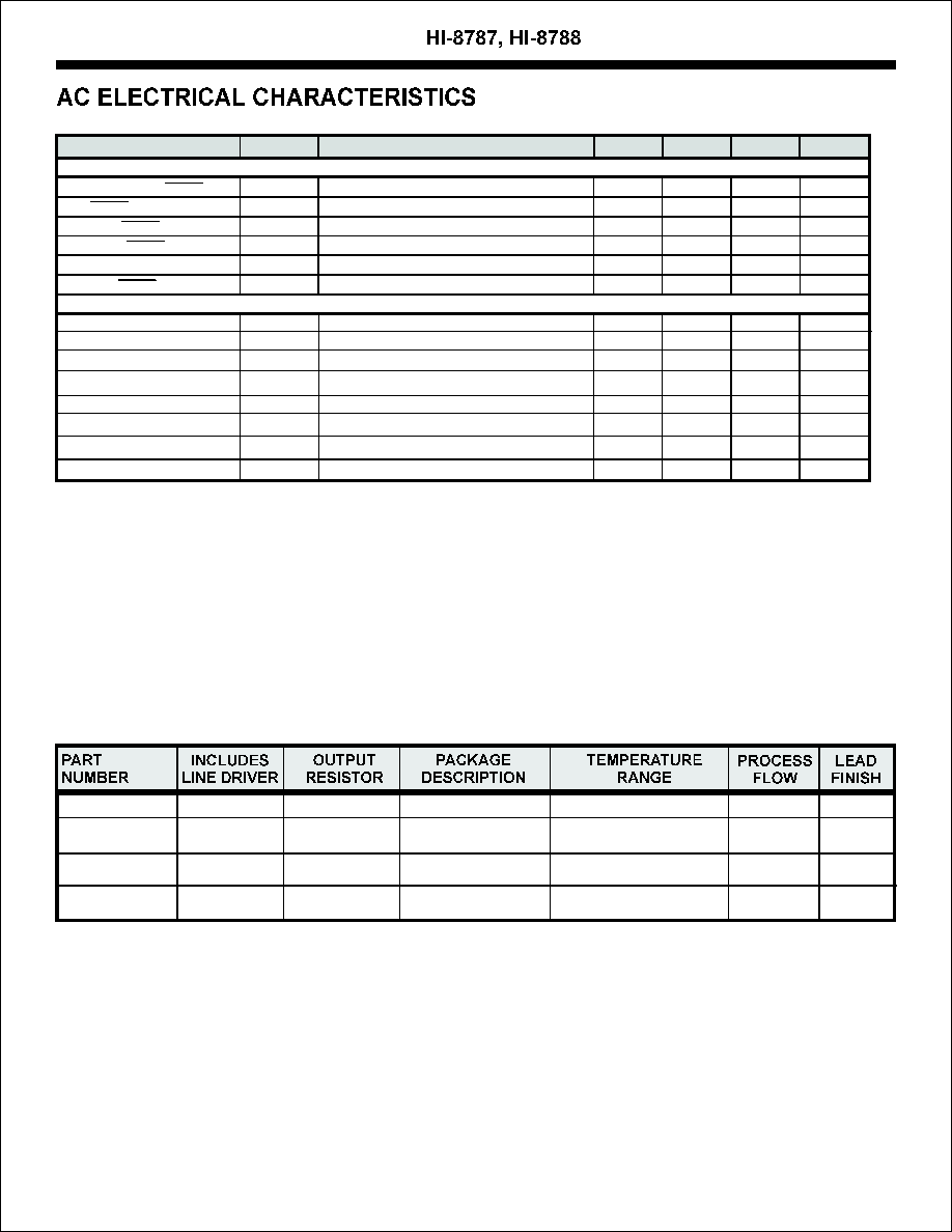
PARAMETER
SYMBOL
CONDITION
MIN
TYP
MAX
UNITS
Operating Voltage
V
4.75
5
5.25
V
Min. Input Voltage
(HI)
V
2.0
1.4
V
Max. Input Voltage
(LO)
V
1.4
0.7
V
Min. Input Current
(HI)
I
V
= 4.9V
280
ĶA
Max. Input Current
(LO)
I
V
= 0.1V
-1
ĶA
Min. Output Voltage
(HI)
V
I
= -1.6mA
2.7
V
Max. Output Voltage
(LO)
V
I
= 1.6mA
0.4
V
Operating Current Drain
I
f = 100khz
0.8
2.8
mA
Input Capacitance
C
Not tested
20
pF
CC
CC
Operating Voltage
V+
9.5
10
10.5
V
Operating Voltage
V-
-9.5
-10
10.5
V
Line Driver Output Levels (Ref. To GND)
ONE
no load, VCC = 5.0V
4.5
5.0
5.5
V
NULL
"
-0.25
0
0.25
V
ZERO
-5.5
-5.0
-4.5
V
Line Driver Output Levels
(Differential TXAOUT - TXBOUT)
ONE
no load, VCC = 5.0V
9.0
10.0
11.0
V
NULL
"
-0.5
0
0.5
V
ZERO
"
-11.0
-10.0
-9.0
V
Minimum Short Circuit Sink or Source Current
I
momentary magnitude
80
mA
Operating Current Drain (V+)
I
f = 100khz
6
20
mA
Operating Current Drain (V-)
I
f = 100khz
-20
-6
mA
IH
IL
IH
IH
IL
IL
OH
OUT
IH
OUT
IN
OUT
DD
EE
NOTE:
Stresses above absolute maximum
ratings or outside recommended operating
conditions may cause permanent damage to the
device. These are stress ratings only. Operation
at the limits is not recommended.
Voltages referenced to Ground
Supply voltages
V+.................................................12.5V
V-.................................................-12.5V
DC current per input pin................ +10ma
Power dissipation at 25į
plastic DIL............1.0W, derate 10mW/įC
ceramic DIL..........0.5W, derate 7mW/įC
Solder Temperature ........275įC for 10 sec
Storage Temperature........-65įC to +150įC
VCC.................................................. 7V
ABSOLUTE MAXIMUM RATINGS
RECOMMENDED OPERATING CONDITIONS
Supply Voltages
V+.......................................+10V... Ī5%
V-........................................ -10V... Ī5%
Temperature Range
Industrial Screening.........-40įC to +85įC
Hi-Temp Screening........-55įC to +125įC
Military Screening..........-55įC to +125įC
VCC....................................... 5V... Ī5%
VCC = 5.0V, V
= 0V, V+ = 10V, V- = -10V, T = Operating Temperature Range (unless otherwise specified).
SS
A
HOLT INTEGRATED CIRCUITS
5
PARAMETER
SYMBOL
TEST CONDITIONS
MIN
TYP
MAX
UNITS
t
20
t
t
t
t
t
Setup Data Bus to
ns
Hold
0
ns
Hold A0 to
0
ns
Pulse width
40
ns
Pulse width A0
40
ns
Delay last
40
ns
Line Driver propagation delay
No load
Output high to low
tphlx
-
500
-
ns
Output low to high
tplhx
-
500
-
ns
Line Driver transition times
Output high to low
t fx
SLP1.5 = logic 1
1.0
1.5
2.0
s
Output low to high
t rx
SLP1.5 = logic 1
1.0
1.5
2.0
s
Output high to low
t fx
SLP1.5 = logic 0
5
10
15
s
Output low to high
t rx
SLP1.5 = logic 0
5
10
15
s
DATA BUS TIMING
LINE DRIVER TIMING
WRITE
SET
to Data Bus
to XMT RDY
WRITE
WRITE
WRITE
WRITE
HLD
AH
WPW
APW
XD
Ķ
Ķ
Ķ
Ķ
VCC = 5.0V, V+ = 10V, V- = -10V, V
= 0V, T =Operating Temperature Range (unless otherwise specified).
SS
A
ORDERING INFORMATION
HI-8787PQI
YES
37.5 ohm
32 Pin Plastic TQFP
-40įC TO +85įC
I
SOLDER
HI-8787PQT
YES
37.5 ohm
32 Pin Plastic TQFP
-55įC TO +125įC
T
SOLDER
HI-8788PQI
YES
10.0 ohm
32 Pin Plastic TQFP
-40įC TO +85įC
I
SOLDER
HI-8788PQT
YES
10.0 ohm
32 Pin Plastic TQFP
-55įC TO +125įC
T
SOLDER
HOLT INTEGRATED CIRCUITS
6
.3543 BSC
(9.00 BSC
)
SQ.
.063 MAX.
(1.60 MAX.
)
.0315 BSC
(0.80 BSC)
.0148
.0030
Ī
(0.375
Ī
)
.075
.0551
.002
Ī
(1.4
Ī
.05)
.0031 R MIN.
(0.08 R MIN.)
.0039
.002
Ī
(0.10
Ī
)
.05
0į
7į
.2755 BSC
(7.00 BSC)
SQ.
See Detail A
Detail A
.0055R
.0024
Ī
(0.14R
Ī
)
.06
.0236
.0059
Ī
(0.60
Ī
)
.15
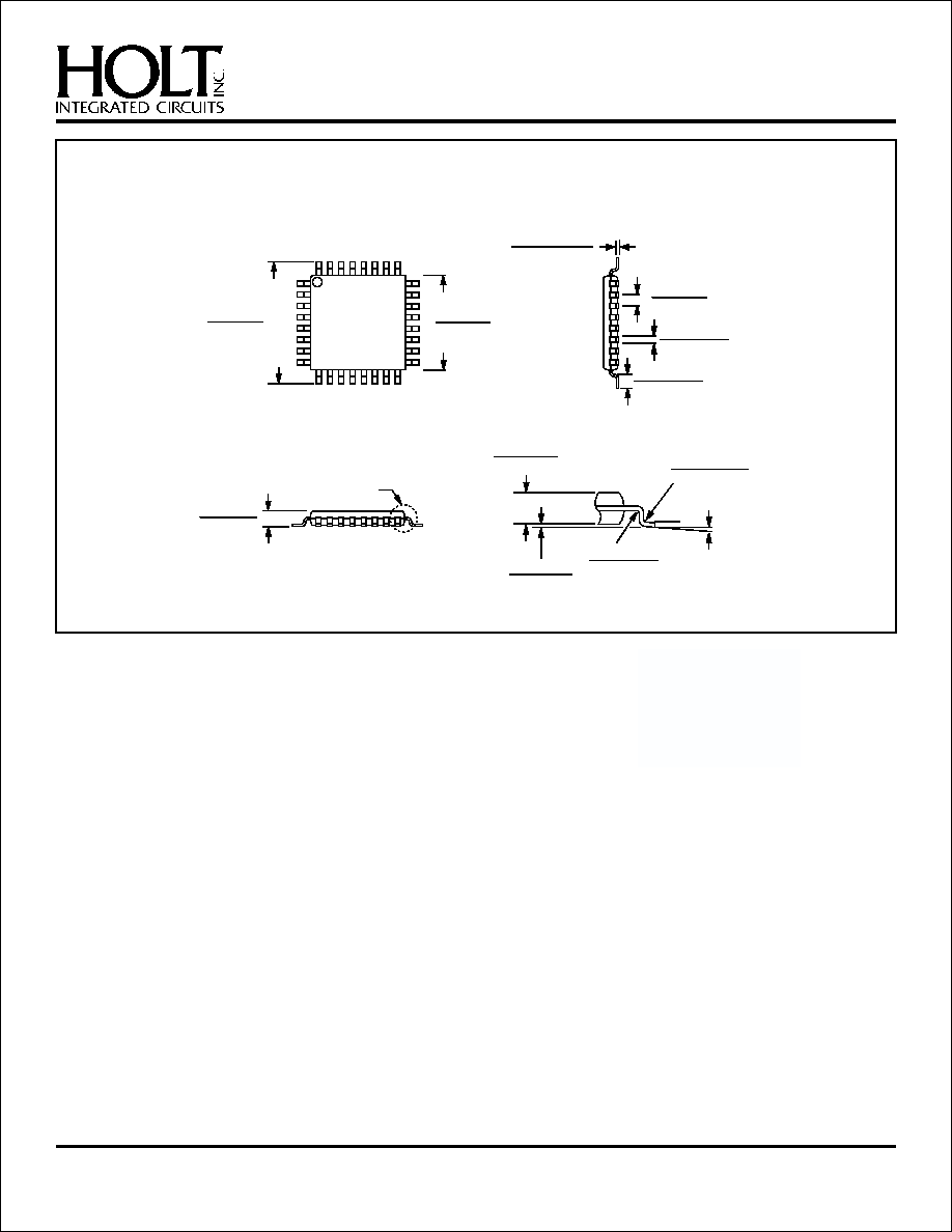
HI-8787, HI-8788 PACKAGE DIMENSIONS
inches (millimeters)
HOLT INTEGRATED CIRCUITS
7
Package Type: 32PTQS
32 PIN PLASTIC THIN QUAD FLAT PACK (TQFP)
.00057
.00022
Ī
(0.0145
Ī
)
.0055