
HRF-AT4510
________________________________________________________________________________________________________
Web Site:
www.mysoiservices.com
Honeywell
Email:
mysoiservices@honeywell.com
Solid State Electronics Center
15.5 dB, DC-4GHz, 5 Bit
Parallel Digital Attenuator
Features
Very Low DC Power Consumption
Attenuation In Steps From 0.5 dB To 15.5 dB
Single Or Dual Power Supply Voltages
Parallel Data Interface
50 Ohm Compatible Impedance
Space Saving LPCC
TM
Surface Mount Packaging
Product Description
The Honeywell HRF-AT4510 is a 5-bit digital
attenuator that is ideal for use in broadband
communication system applications that require
accuracy, speed and low power consumption. The
HRF-AT4510 is manufactured with Honeywell's
patented Silicon On Insulator (SOI) CMOS
manufacturing technology, which provides the
performance of GaAs with the economy and
integration capabilities of conventional CMOS.
HRF-AT4510 in LPCCTM Package
RF Electrical Specifications @ + 25
o
C
Parameter
Test Condition
Frequency
Minimum
Typical
Maximum
Units
Insertion Loss
DC � 0.5 GHz
2.0 GHz
3.0 GHz
4.0 GHz
1.60
2.00
2.40
4.40
2.20
2.40
2.90
5.00
dB
dB
dB
dB
1dB Compression
VSS = 0V, Input Power
1.0 GHz
2.0 GHz
22.5
21.0
dBm
dBm
1dB Compression
VSS = - 3, Input Power
1.0 GHz
2.0 GHz
28.5
27.0
dBm
dBm
Input IP3
VSS = 0V Two-tone inputs
Up To +5 dBm @ 0 dB
Attenuation
2.0 GHz
36.0
dBm
Input IP3
V
ss
= - 3
Two-tone inputs Up To + 5
dBm @ 0 dB Attenuation
2.0 GHz
>36.0
dBm
Return Loss*
Any Bit or Combination of
Bits
DC - 4.0 GHz
-11
-15
dB
Attenuation Accuracy
All attenuation states
All attenuation states
All attenuation states
All attenuation states
DC - 1.0 GHz
2.0 GHz
3.0 GHz
4.0 GHz
+/-(0.17 + 3% of programmed IL)
+/-(0.22 + 3% of programmed IL)
+/-(0.33 + 3% of programmed IL)
+/-(0.45 + 3% of programmed IL)
dB
dB
dB
dB
Trise, Tfall*
Ton, Toff (Tpd)
Transients
10% To 90%
50% Cntl To 90%/10%RF
In-Band
10
15
30
nS
nS
mV
0.01uF Decoupling Capacitors Required On Power Supply Rails.
*By design
12001 State Highway 55
2002 4510W
Published February 2003 Page 1
Plymouth, Minnesota 55441-4799
1-800-323-8295

HRF-AT4510
________________________________________________________________________________________________________
Web Site:
www.mysoiservices.com
Honeywell
Email:
mysoiservices@honeywell.com
Solid State Electronics Center
Functional Schematic
RF In
RF Out
S4
S3
S0
S1
S2
8dB
4dB
2dB
1dB
.5dB
ESD, Buffer, Level Shift
DC Electrical Specifications @ + 25
o
C
Parameter
Minimum
Typical
Maximum
Units
V
DD
3.3
1
5.0
V
V
SS
-5.0
V
I
DD
Power Supply Current
35
uA
CMOS Logic level (0)
0
0.8
V
CMOS Logic level (1)
V
DD
� 0.8
V
DD
V
Input Leakage Current
10
uA
Note 1, performance curves are for V
DD
= +5.0 +/- 10%
Absolute Maximum Ratings
2
.
Parameter
Absolute Maximum
Units
Input Power
+ 35
dBm
V
DD
+6.0
V
V
SS
-5.5
V
ESD Voltage
400
V
Operating Temperature
-40 To +85
Degrees C
Storage Temperature
-65 To +125
Degrees C
Digital Inputs
V
DD
+0.6 max to -0.6 min
V
(Note 2) Operation of this Device beyond any of these parameters may cause permanent damage.
Latch-Up: Unlike conventional CMOS digital attenuators, Honeywell's HRF-AT4510 is immune to latch-up.
ESD Protection: Although the HRF-AT4510 contains ESD protection circuitry on all digital inputs, conventional precautions should
be taken to ensure that the Absolute Maximum Ratings are not exceeded.
12001 State Highway 55
2002 4510W
Published February 2003 Page 2
Plymouth, Minnesota 55441-4799
1-800-323-8295

HRF-AT4510
________________________________________________________________________________________________________
Web Site:
www.mysoiservices.com
Honeywell
Email:
mysoiservices@honeywell.com
Solid State Electronics Center
Package Outline Drawing
4.0 mm
4.0 mm
This package conforms to the LPCC
TM
4 X 4 mm 24 lead body dimensions.
See ASAT LPCC Marketing Outline Dwg. # DGMJ00004 Latest Rev. at
http://www.asat.com
for additional dimensional information
Pin Configuration
Pin
Function
Pin
Function
1
VDD
13
GROUND
2
GROUND
14
GROUND
3
GROUND
15
RF OUTPUT
4
RF INPUT
16
GROUND
5
GROUND
17
VSS
6
GROUND
18
DIGITAL GROUND
7
GROUND
19
S0
8
GROUND
20
S1
9
GROUND
21
S2
10
GROUND
22
S3
11
GROUND
23
S4
12
GROUND
24
OPEN
Note: Bottom ground plate must be grounded for proper RF performance.
Truth Table
S4
S3
S2
S1
S0
Output
0
0
0
0
0
1
1
0
0
0
0
1
0
1
0
0
0
1
0
0
1
0
0
1
0
0
0
1
0
1
0
0
0
0
1
Reference Input
0.5 dB
1 dB
2 dB
4 dB
8 dB
15.5 dB
Operation: Data on parallel input "S" pins are independently buffered and presented to the RF attenuator circuits.
"0" = CMOS Low, "1" = CMOS High.
12001 State Highway 55
2002 4510W
Published February 2003 Page 3
Plymouth, Minnesota 55441-4799
1-800-323-8295
HRF-AT4510
________________________________________________________________________________________________________
Web Site:
www.mysoiservices.com
Honeywell
Email:
mysoiservices@honeywell.com
Solid State Electronics Center
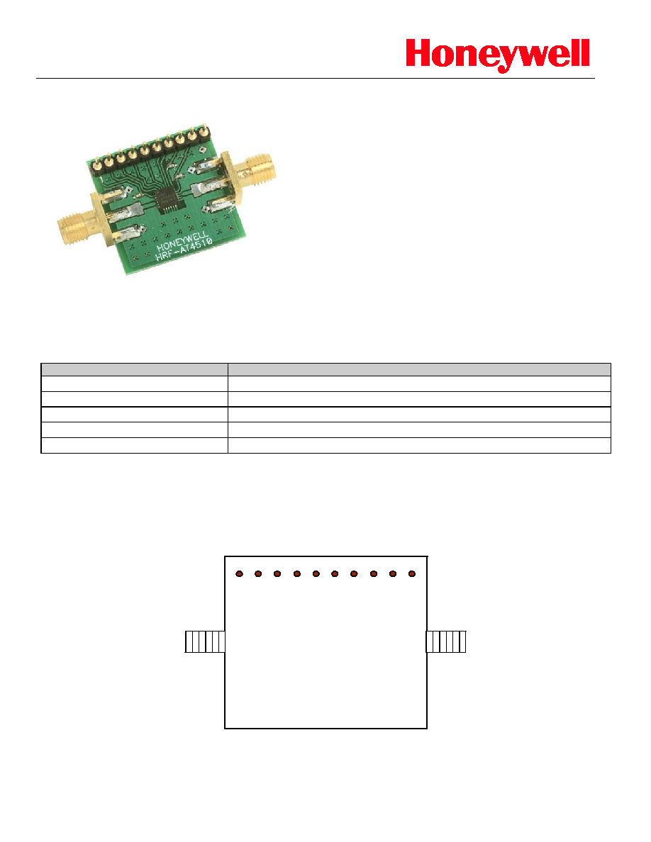
Evaluation Circuit Board
HRF-AT4510 Evaluation Board
Honeywell's evaluation board provides an
easy to use method of evaluating the RF
performance of our attenuator. Simply
connect power, DC and RF signals to be
measuring attenuator performance in less
than 10 minutes.
Evaluation Circuit Board Layout Design Details
Item
Description
PCB
Impedance Matched Multi-Layer FR4
Attenuator
HRF-AT4510 Digital Attenuator
Chip Capacitor
Panasonic Model ECU-E1C103KBQ Capacitor, .01uf 0402 10% 16V
RF Connector
Johnson Connectors Model 142-0701-801 SMA RF Coaxial Connector
DC Pin
Mil-Max Model 800-10-064-10-001 Header Pins
Evaluation Circuit Board Connections
HRF-AT4510
Evaluation Board
Top View
HRF-AT4510
Honeywell
VDD
VSS
Digital
Gnd
RF In
RF Out
S0
S1
S2
S3
S4
Open
Gnd
12001 State Highway 55
2002 4510W
Published February 2003 Page 4
Plymouth, Minnesota 55441-4799
1-800-323-8295

HRF-AT4510
___
________________________
Web Site:
www.mysoiservices.com
Honeywell
Email:
mysoiservices@honeywell.com
Solid State Electronics Center
12001 State Highway 55
2002 4510W
Published February 2003 Page 5
Plymouth, Minnesota 55441-4799
1-800-323-8295
Performance Curves
Insertion Loss
AT4510 Insertion Loss By Attenuation State Vs Frequency
-20
-18
-16
-14
-12
-10
-8
-6
-4
-2
0
0
0.5
1
1.5
2
2.5
3
3.5
4
Frequency (GHz)
Insertion Loss (dB)
S12(00000)
S12(00001)
S12(00010)
S12(00011)
S12(00100)
S12(00101)
S12(00110)
S12(00111)
S12(01000)
S12(01001)
S12(01010)
S12(01011)
S12(01100)
S12(01101)
S12(01110)
S12(01111)
S12(10000)
S12(10001)
S12(10010)
S12(10011)
S12(10100)
S12(10101)
S12(10110)
S12(10111)
S12(11000)
S12(11001)
S12(11010)
S12(11011)
S12(11100)
S12(11101)
S12(11110)
S12(11111)
Return Loss
_____________________________________________________________________________
AT4510 Return Loss By Attenuation State Vs Frequency
-60
-50
-40
-30
-20
-10
0
0
0.5
1
1.5
2
2.5
3
3.5
4
Frequency (GHz)
S11 Return Loss (dB)
S11(00000)
S11(00001)
S11(00010)
S11(00011)
S11(00100)
S11(00101)
S11(00110)
S11(00111)
S11(01000)
S11(01001)
S11(01010)
S11(01011)
S11(01100)
S11(01101)
S11(01110)
S11(01111)
S11(10000)
S11(10001)
S11(10010)
S11(10011)
S11(10100)
S11(10101)
S11(10110)
S11(10111)
S11(11000)
S11(11001)
S11(11010)
S11(11011)
S11(11100)
S11(11101)
S11(11110)
S11(11111)