
HRF-SW1001
________________________________________________________________________________________________________
Web Site:
www.mysoiservices.com
Honeywell
Email:
mysoiservices@honeywell.com
Solid State Electronics Center
SPDT Absorptive RF Switch
Features
High Isolation Of > 40 dB @ 2 GHz
Low Insertion Loss Of 1.1dB @ 2 GHz
DC To 2.5 GHz Operating Frequency
Integrated CMOS Control Logic
Integrated ESD Protection on Digital I/O
Single Positive Supply Voltage
Ultra Small LPCC
TM
Packaging
Impedance matched for 75 Ohm systems
Product Description
The Honeywell HRF-SW1001 is a high performance
single pole double throw (SPDT) absorptive RF switch
that is ideal for use in wireless basestation and handset
applications that require minimum power and minimum
insertion loss.
The HRF-SW1001 is manufactured with Honeywell's
patented Silicon On Insulator (SOI) CMOS technology,
which provides the performance of GaAs with the
economy and integration capabilities of conventional
CMOS technology.
HRF-SW1001 in LPCC
TM
Package
RF Electrical Specifications @ + 25
o
C
Results @ Vdd=5.0 =/- 10%, Vss = 0 unless otherwise stated, Z
0
=75 ohms
Parameter
Test Condition
Frequency
Minimum
Typical
Maximum
Units
Insertion Loss*
DC � 0.5 GHz
2.0 GHz
2.5 GHz
0.8
0.9
1.1
1.1
1.4
1.5
dB
dB
dB
Isolation*
DC � 0.5 GHz
2.0 GHz
2.5 GHz
52
45
41
55
49
44
dB
dB
dB
VSWR*
DC � 0.5 GHz
2.0 GHz
2.5 GHz
1.1:1
1.2:1
1.3:1
1.4:1
Ratio
Ratio
Ratio
1dB Compression*
Input Power
Vss=Gnd
Vss= -3
1.0 GHz
1.0 GHz
21
29
dBm
dBm
Input IP3*
Two-Tone Inputs Up To + 5 dBm
Vss=Gnd
Vss= -3
2.0 GHz
2.0 GHz
35
35
dBm
dBm
Trise, Tfall*
Ton, Toff
Transients
10% To 90%
50% Cntl To 90%/10%Rf
In-Band
10
20
10
nS
nS
mV
*Guaranteed by design
12001 State Highway 55
2002 1001W
Published February 2003 Page 1
Plymouth, Minnesota 55441-4799
1-800-323-8295

HRF-SW1001
_______________________________________________________________
Web Site:
www.mysoiservices.com
Honeywell
Email:
mysoiservices@honeywell.com
Solid State Electronics Center
12001 State Highway 55
2002 1001W
Published February 2003 Page 2
Plymouth, Minnesota 55441-4799
1-800-323-8295
DC Electrical Specifications @ + 25
o
C
Parameter
Minimum
Typical
Maximum
Units
Single V
DD
Supply Voltage
3.3*
5.0
5.5
V
V
SS
-5.0
V
Idd
.07
10
uA
CMOS Logic Level (0)
0
0.8
V
CMOS Logic Level (1)
V
DD
� 0.8
V
DD
V
Input Leakage Current
10
uA
* Performance curves are for Vdd = +5.0 +/- 10%
Absolute Maximum Ratings
1
Parameter
Absolute Maximum
Units
V
DD
+6.0
V
V
SS
-5.5
V
Vin Digital Logic 0
- 0.6
V
Vin Digital Logic 1
Vdd + 0.6
V
Maximum Input Power
> 35
dBm
ESD Voltage
400
V
Operating Temperature Range
+85
Degrees C
Storage Temperature Range
+125
Degrees C
(Note 1) Operation beyond any of these parameters may cause permanent damage.
Latch-Up: Unlike conventional CMOS RF switches, Honeywell's HRF-SW1001 is immune to latch-up.
ESD Protection: Although this device contains ESD protection circuitry on all digital inputs, conventional precautions should be
taken to ensure that the Absolute Maximum Ratings are not exceeded.
Package Outline Drawing
_________________________________________
3 mm
3 mm
Bottom View, 12 Pin 3X3 mm LPCC
TM
Package
ASAT LPCC Marketing Outline Dwg. # GMJ00004
For more information see
http://www.asat.com
HRF-SW1001
________________________________________________________________________________________________________
Web Site:
www.mysoiservices.com
Honeywell
Email:
mysoiservices@honeywell.com
Solid State Electronics Center
Truth Table
Switch Control
RF Output 1
RF Output 2
0
1
RF INPUT
- - -
- - -
RF INPUT
"0" = CMOS Low, "1" = CMOS High
Pin Configuration
Pin
Function
Pin
Function
1
GROUND
7
GROUND
2
RF OUT 2
8
RF OUT 1
3
GROUND
9
GROUND
4
VDD
10
GROUND
5
SWITCH CONTROL
11
RF IN
6
VSS
12
GROUND
Note: Bottom ground plate must be grounded for proper RF performance.
Evaluation Circuit Board Connections
HRF-SW1001
Evaluation Board
Top View
Honeywell HRF-SW1001
Ground
VDD
SW
Control
VSS
Ground
RF Out2
RF Out1
RF In
12001 State Highway 55
2002 1001W
Published February 2003 Page 3
Plymouth, Minnesota 55441-4799
1-800-323-8295
HRF-SW1001
________________________________________________________________________________________________________
Web Site:
www.mysoiservices.com
Honeywell
Email:
mysoiservices@honeywell.com
Solid State Electronics Center
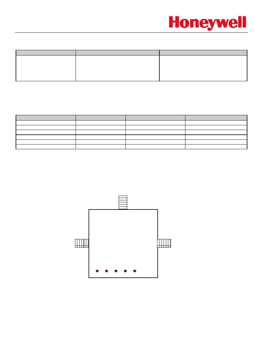
Performance Curves
Insertion Loss
Insertion Loss Versus Frequency
-3.0
-2.5
-2.0
-1.5
-1.0
-0.5
0.0
0.0
0.5
1.0
1.5
2.0
2.5
3.0
3.5
Frequency (GHz)
Insertion Loss (dB)
The Insertion Loss curve shows the
typical return loss versus frequency at
Vdd = +5.0 +/- 10%, Ta = 25C, Z
0
= 75
Ohms
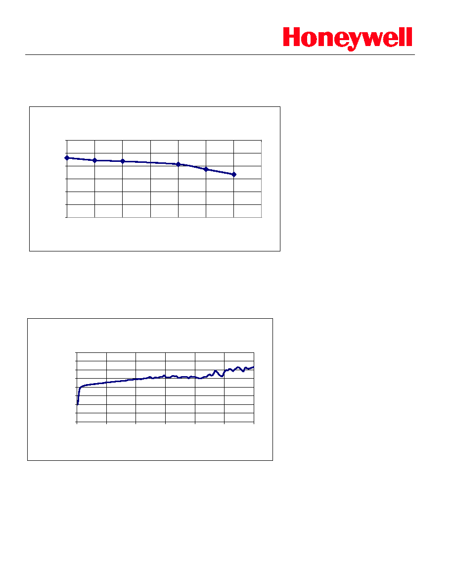
Isolation
Isolation Versus Frequency
-100.0
-90.0
-80.0
-70.0
-60.0
-50.0
-40.0
-30.0
-20.0
0.0
0.5
1.0
1.5
2.0
2.5
3.0
Frequency [GHz]
Isolation [dB]
The Isolation curve shows the
typical isolation of an "off" state
output to the insertion path.
12001 State Highway 55
2002 1001W
Published February 2003 Page 4
Plymouth, Minnesota 55441-4799
1-800-323-8295

HRF-SW1001
________________________________________________________________________________________________________
Web Site:
www.mysoiservices.com
Honeywell
Email:
mysoiservices@honeywell.com
Solid State Electronics Center
Return Loss
Input/Output Return Losses Versus Frequency
-40
-35
-30
-25
-20
-15
-10
-5
0
0
0.5
1
1.5
2
2.5
3
Frequency [GHz]
Return Loss [dB]
S11
The return loss curve shows
the input return loss S11 and
the output return loss in the
insertion path S22.
S22
Evaluation Circuit Board
HRF-SW1001 Evaluation Board
Honeywell's evaluation board provides
an easy to use method of evaluating the
RF performance of our switch. Simply
connect power, DC and RF signals to
be measuring switch performance in
less than 10 minutes.
12001 State Highway 55
2002 1001W
Published February 2003 Page 5
Plymouth, Minnesota 55441-4799
1-800-323-8295