
GM6535
1
GM6535
60 MHz Universal Programmable
Dual PLL Frequency synthesizer
GENERAL DESCRIPTIONS
The GM6535 is a dual phase ≠ locked loop
(PLL) frequency synthesizer especially designed for
CT-1 cordless phone applications worldwide. This
frequency synthesizer is also for any products with
frequency operation at 60 MHz or below.
The device features fully programmable
receive, transmit, reference, and auxiliary reference
counters accessed through an MCU serial interface,
this feature allows this device to operate in any CT-
1 cordless phone application.
The device consists of two independent phase
detectors for transmit and receive loops. A common
reference oscillator, driving two independent
reference frequency counters, provides independent
reference frequencies for transmit and receive loops.
The auxiliary reference counter allows the
user to select an additional reference frequency for
receive and transmit loops if required.
FEATURES
∑ Operating Voltage Range: 2.5 to 5.5 V
∑ Operating Temperature Range:-40 to +75° …
∑ Operating Power Consumption:3.0mA@2.5V
∑ Maximum Operating Frequency:
60MHz@200mV
p-p
, V
DD
=2.5V
∑ 3 or 4 Pins Used for serial MCU Interface
∑ Power Saving Mode Controlled by MCU
∑ Lock Detect Signal
∑ On-Chip Reference Oscillator Supports External
Crystals to 16.0 MHz
∑ Reference Frequency Counter Division Range: 16 to
4095
∑ Auxiliary Reference Frequency Counter Division
Range: 16 to 16,383
∑ Transmit Counter Division Range:16 to 65,535
∑ Receive Counter Division Range: 16 to 65,53
PIN CONFIGURATION
ABSOLUTE MAXIMUM RATINGS (Voltages Referenced to v
ss
)
Symbol
Ranting
Value
Unit
V
DD
DC Supply Voltage
-0.5 to +6.0
V
V
in
Input Voltage, all Inputs
-0.5 to V
DD
+0.5
V
I
in
, I
out
DC Current Drain Per Pin
10
mA
I
DD
, I
SS
DC Current Drain V
DD
or V
SS
Pins
30
mA
T
stg
Storage Temperature Range
-65 to + 150
° …
CLK
D in
AD in
ENB
MCUCLK
Vss
OSC
out
OSC
i
LD
Tx PD
OUT
f
in-T
TxPS/f
Tx
VDD
RxPS/f
Rx
RxPD
o
CLK
D in
AD in
ENB
MCUCLK
Vss
OSC
out
OSC
i
LD
Tx PD
OUT
TxPS/f
Tx
VDD
RxPS/f
Rx
RxPD
o
1
2
3
4
5
6
7
8
9
10
11
12
13
14
15
16
2
3
4
5
6
7
8
9
10
11
12
13
14
15
16
1
16DIP
16 SOP (150Mil)
f
in-R
f
in-R
f
in-T
GM6535
3
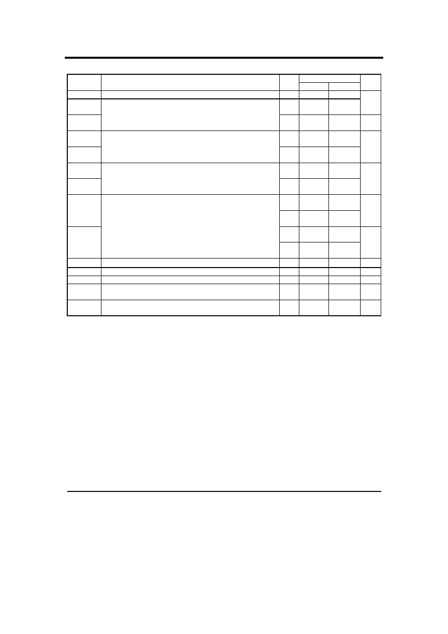
ELECTRICAL CHARACTERISTICS (Voltages Referenced to V
SS
, T
A
=25 ° …
)
Guaranteed Limit
Symbol
Characteristic
V
DD
Min
Max
Unit
V
DD
Power Supply Voltage
-
2.5
5.5
V
OL
2.5
5.5
-
-
0.1
0.1
V
V
OH
Output Voltage 0 Level
(I
out
= 0)
(V
in
=V
DD
or 0) 1 Level
2.5
5.5
2.45
5.45
-
-
V
V
IL
2.5
5.5
-
-
0.75
1.65
V
IH
Input Voltage 0 Level
(V
out
0.5 V or V
DD
≠ 0.5V)
1 Level
2.5
5.5
1.75
3.85
-
-
V
V
OH
2.5
5.5
-0.18
-0.55
-
-
I
OL
Output Current (V
out
= 2.2V) Source
(V
out
= 5.0V)
(V
out
= 0.3V) Sink
(V
out
= 0.5V)
2.5
5.5
0.18
0.55
-
-
mA
2.5
5.5
-
-
-30
-66
I
IL
2.5
5.5
-
-
-1.0
-1.0
• Ï
A
2.5
5.5
-
-
30
61
I
IH
Input Current OSC
in
, f
in-T
, f
in-R
(V
in
= 0)
AD
in
, CLK , D
in
, ENB
(V
in
= V
DD
≠0.5)
OSC
in
, f
in-T
, f
in-R
AD
in
, CLK , D
in
, ENB
2.5
5.5
-
-
5.0
5.0
• Ï
A
I
OZ
Three-Stats Leakage Current (V
out
= 0 V or 5.5 V)
5.5
-
° æ
100
nA
C
in
Input Capacitance
-
-
8.0
pF
C
out
Output Capacitance
-
-
8.0
pF
I
DD
(standby)
Standby Current
(All Counters are in Power-Down Mode with Oscillator On)
2.5
5.5
-
-
0.3
1.5
mA
I
DD
Operating Current (200mV
p-p
input at f
in-T
= 60MHz, and f
in-R
=60MHz, OSC = 10.24MHz)
2.5
5.5
-
-
3.0
10
mA

GM6535
4
SWITCHING CHARACTERISTICS (T
A
= 25° …
, C
L
= 50 pF)
Symbol
Characteristic
Figure # V
DD
Min Max Unit
t
TLH
Output Rise Time
1
2.5
5.5
-
-
200
100
ns
t
THL
Output Fall Time
1
2.5
5.5
-
-
200
100
ns
t
T
, t
f
Input Rise and Fall Time, OSC
in
2
2.5
5.5
-
-
5.0
4.0
µs
t
W
Input Pulse Width, CLK and ENB
3
2.5
5.5
80
60
-
-
ns
f
max
Input frequency OSC
in
(Input = Sine Wave @
200mV
p-p
f
in-T
f
in-R
2.5-5.5
2.5-5.5
2.5-5.5
-
-
-
16
60
60
MHz
t
su
Setup Time Data to CLK
ENB to CLK
5
2.5-5.5
5.5-5.5
100
200
-
-
ns
t
h
Hold Time, CLK to Data
5
2.5
5.5
80
40
-
-
ns
t
rec
Recovery Time, ENB to CLK
5
2.5
5.5
80
40
-
-
ns
t
sul
Setup Time, ENB to CLK
4
2.5-5.5 80
-
ns
t
hl
Hold Time, CLK to ENB
4
2.5-5.5 600
-
ns
SWITCHING WAVERORMS
t
TLH
90%
10%
t
THL
t
r
t
f
90%
10%
V
SS
t
W
50%
V
DD
V
DD
V
SS
ANY
OUTPUT
Figure 1
.
CLK, OSC
in
f
in-T,
f
in-R
ENB, CLK
Figure 2.
Figure 3.

