4,194,304 WORDS x 4 BIT
CMOS DYNAMIC RAM
Description
The GM71V(S)17403C/CL is the new
generation dynamic RAM organized 4,194,304
words x 4 bit. GM71V(S)17403C/CL has
realized higher density, higher performance and
various functions by utilizing advanced CMOS
process technology. The GM71V(S)17403C/CL
offers Extended Data Out (EDO) Page Mode as
a high speed access mode. Multiplexed address
inputs permit the GM71V(S)17403C/CL to be
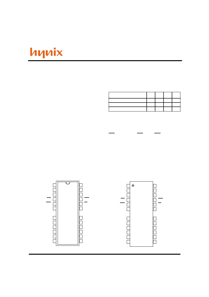
packaged in a standard 300 mil 24(26) pin SOJ,
and a standard 300 mil 24(26) pin plastic TSOP
II. The package size provides high system bit
densities and is compatible with widely
available automated testing and insertion
equipment. System oriented features include
single power supply 3.3V +/- 0.3V tolerance,
d i r e c t i n t e r f a c i n g c a p a b i l i t y w i t h h i g h
performance logic families such as Schottky
TTL.
Features
* 4,194,304 Words x 4 Bit Organization
* Extended Data Out Mode Capability
* Single Power Supply (3.3V +/- 0.3V)
* Fast Access Time & Cycle Time
* Low Power
Active : 432/369/360mW (MAX)
Standby : 7.2mW (CMOS level : MAX)
: 0.36mW (L-version : MAX)
* RAS Only Refresh, CAS before RAS Refresh,
Hidden Refresh Capability
*All inputs and outputs TTL Compatible
* 2048 Refresh Cycles/32ms
* 2048 Refresh Cycles/128ms (L-version)
* Self Refresh Operation (L-version)
* Battery Backup Operation (L-version)
* Test Function : 16bit parallel test mode
GM71V(S)17403C/CL-5
GM71V(S)17403C/CL-6
GM71V(S)17403C/CL-7
t
RAC
t
CAC
t
RC
t
HPC
50
60
13
15
84
104
20
25
70
18
124
30
(Top View)
Pin Configuration
24(26) SOJ
V
CC
I/O1
I/O2
WE
RAS
NC
A10
A0
A1
A2
A3
V
CC
V
SS
I/O4
I/O3
CAS
OE
A9
A8
A7
A6
A5
A4
V
SS
1
2
3
4
5
6
8
9
10
11
12
13
14
15
16
17
18
19
21
22
23
24
25
26
24(26) TSOP II
V
CC
I/O1
I/O2
WE
RAS
A11
A10
A0
A1
A2
A3
V
CC
V
SS
I/O4
I/O3
CAS
OE
A9
A8
A7
A6
A5
A4
V
SS
1
2
3
4
5
6
8
9
10
11
12
13
14
15
16
17
18
19
21
22
23
24
25
26
(Unit: ns)
GM71V17403C
GM71VS17403CL
Rev 0.1 / Apr'01
GM71V17403C
GM71VS17403CL
Rev 0.1 / Apr'01
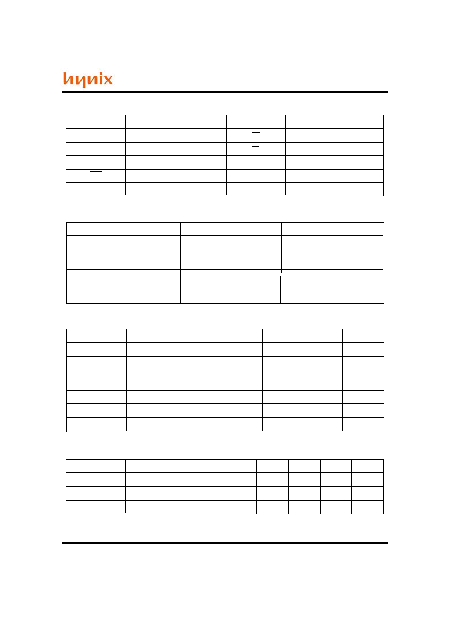
Pin Description
Pin
Function
Pin
Function
A0-A10
A0-A10
I/O1-I/O4
V
CC
V
SS
Address Inputs
Refresh Address Inputs
Data Input/Data Output
Row Address Strobe
Column Address Strobe
Read/Write Enable
Output Enable
Power (+3.3V)
Ground
Ordering Information
Type No.
Access Time
Package
GM71V(S)17403CJ/CLJ-5
GM71V(S)17403CJ/CLJ-6
GM71V(S)17403CJ/CLJ-7
50ns
60ns
70ns
300 Mil
24(26) Pin
Plastic SOJ
GM71V(S)17403CT/CLT-5
GM71V(S)17403CT/CLT-6
GM71V(S)17403CT/CLT-7
300 Mil
24(26) Pin
Plastic TSOP II
Absolute Maximum Ratings
Symbol
Parameter
Rating
Unit
T
A
T
STG
V
IN/OUT
V
CC
I
OUT
0 ~ 70
-55 ~ 125
-0.5 ~ Vcc+0.5
(<=4.6V(MAX))
-0.5 ~ 4.6
50
Ambient Temperature under Bias
Storage Temperature
Voltage on any Pin Relative to V
SS
Supply Voltage Relative to V
SS
Short Circuit Output Current
V
V
mA
P
D
1.0
Power Dissipation
W
Note: All voltage referred to Vss.
RAS
CAS
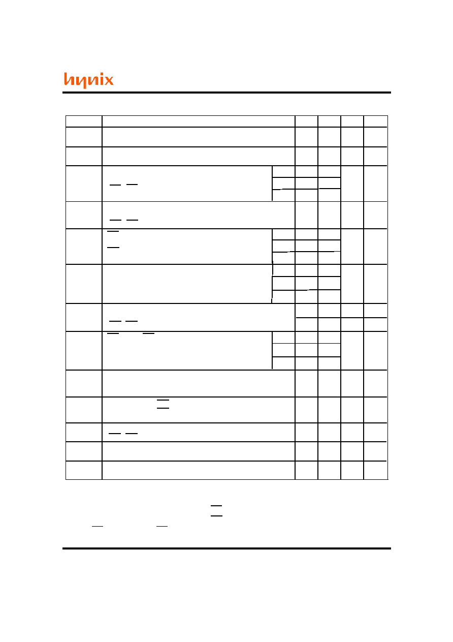
Recommended DC Operating Conditions (T
A
= 0 ~ 70C)
Symbol
Parameter
Unit
V
CC
V
IH
V
IL
Supply Voltage
Input High Voltage
Input Low Voltage
V
V
V
Max
3.6
V
CC
+ 0.3
0.8
Typ
3.3
-
-
Min
3.0
2.0
-0.3
C
C
NC
No Connection
OE
WE
50ns
60ns
70ns
GM71V17403C
GM71VS17403CL
Rev 0.1 / Apr'01
DC Electrical Characteristics (V
CC
= 3.3V+/-0.3V, V
SS
= 0V, T
A
= 0 ~ 70C)
Symbol
Parameter
Note
V
OH
V
OL
Output Level
Output "H" Level Voltage (I
OUT
=
-2mA
)
Unit
Max
V
CC
0.4
Min
2.4
0
Output Level
Output "L" Level Voltage (I
OUT
=
2
mA)
I
CC1
Operating Current
Average Power Supply Operating Current
(RAS, CAS Cycling
:
t
RC
=
t
RC
min)
I
CC2
Standby Current (TTL)
Power Supply Standby Current
(RAS, CAS = V
IH
,
D
OUT
=
High-Z)
I
CC3
RAS Only Refresh Current
Average Power Supply Current
RAS Only Refresh Mode
(t
RC
=
t
RC
min)
I
CC4
I
CC5
Standby Current (CMOS)
Power Supply Standby Current
(RAS, CAS >= V
CC
- 0.2V, D
OUT
= High-Z)
1
-
I
CC6
CAS-before-RAS Refresh Current
(t
RC
=
t
RC
min)
I
CC7
100
-
I
CC8
I
L(I)
10
-10
I
L(O)
10
-10
Input Leakage Current
Any Input (0V
<=
V
IN
<=
4.6V)
Output Leakage Current
(D
OUT
is Disabled, 0V
<=
V
OUT
<= 4.
6V)
I
CC9
Self-Refresh Mode Current
(RAS, CAS<=0.2V
,
D
OUT
=
High-Z, CMOS interface)
200
-
EDO Page Mode Current
Average Power Supply Current
EDO Page Mode
(t
HPC
= t
HPC
min)
Note: 1. I
CC
depends on output load condition when the device is selected.
I
CC
(max) is specified at the output open condition.
2. Address can be changed once or less while RAS = V
IL
.
3. Address can be changed once or less while CAS = V
IH
.
4. CAS = L (<=0.2) while RAS = L (<=0.2).
5. L - Version.
100
-
50ns
60ns
70ns
90
80
-
2
-
-
100
-
50ns
60ns
70ns
90
80
-
-
-
90
-
50ns
60ns
70ns
80
75
-
V
V
mA
uA
uA
uA
-
Standby Current RAS = V
IH
CAS = V
IL
D
OUT
=
Enable
5
1
mA
Battery Backup Operating Current(Standby with CBR Refresh)
(CBR refresh, t
RC
= 31.3us
,
t
RAS
<=
0.3
us,
D
OUT
=
High-Z, CMOS interface)
300
-
uA
4,5
uA
5
5
mA
1, 2
mA
mA
2
mA
1, 3
mA
100
-
50ns
60ns
70ns
-
-
90
80

GM71V17403C
GM71VS17403CL
Rev 0.1 / Apr'01
Capacitance (V
CC
= 3.3V +/- 0.3V, T
A
= 25C)
AC Characteristics (V
CC
= 3.3V +/- 0.3V, V
SS
= 0V, T
A
= 0 ~ 70C, Notes 1, 2, 18)
Read, Write, Read-Modify-Write and Refresh Cycles (Common Parameters)
Symbol
Parameter
Note
C
I1
C
I2
C
I/O
Input Capacitance (Address)
Input Capacitance (Clocks)
Output Capacitance (Data-In/Out)
1
1
1, 2
Unit
pF
pF
pF
Max
5
7
7
Min
-
-
-
Test Conditions
Input rise and fall times : 2ns
Input levels : V
IL
= 0V, V
IH
= 3V
Input timing reference levels : 0.8V, 2.0V
Output timing reference levels : 0.8V, 2.0V
Output load : 1 TTL gate + C
L
(100pF)
(Including scope and jig)
Note: 1. Capacitance measured with Boonton Meter or effective capacitance measuring method.
2. CAS = V
IH
to disable D
OUT
.
Symbol
Parameter
Note
Max
Unit
Min
Max
Min
Max
Min
t
RC
Random Read or Write Cycle Time
84
-
104
-
124
-
t
RP
RAS Precharge Time
30
-
40
-
50
-
t
RAS
RAS Pulse Width
50
10,000
60
10,000
70
10,000
t
CAS
CAS Pulse Width
8
10,000
10,000
10,000
10
13
t
ASR
Row Address Set up Time
0
-
-
-
0
0
t
RAH
Row Address Hold Time
8
-
-
-
10
10
t
ASC
Column Address Set-up Time
0
-
-
-
0
0
t
CAH
Column Address Hold Time
8
-
-
-
10
13
t
RCD
RAS to CAS Delay Time
12
37
45
52
14
14
3
t
RAD
RAS to Column Address Delay Time
10
25
30
35
12
12
4
t
RSH
RAS Hold Time
10
-
-
-
13
13
t
CSH
CAS Hold Time
35
-
-
-
40
45
t
CRP
CAS to RAS Precharge Time
5
-
-
-
5
5
t
T
Transition Time (Rise and Fall)
2
50
50
50
2
2
7
t
DZO
OE Delay Time from D
IN
0
-
-
-
0
0
t
DZC
CAS Delay Time from D
IN
0
-
-
-
0
0
GM71V(S)17403
C/CL-5
OE to D
IN
Delay Time
13
-
-
-
15
18
5
6
6
t
CP
CAS Precharge Time
8
-
10
-
13
-
t
ODD
GM71V(S)17403
C/CL-6
GM71V(S)17403
C/CL-7
ns
ns
ns
ns
ns
ns
ns
ns
ns
ns
ns
ns
ns
ns
ns
ns
ns
ns
GM71V17403C
GM71VS17403CL
Rev 0.1 / Apr'01
Read Cycle
Symbol
Parameter
Unit
Max
Note
Min
Max
Min
t
RAC
Access Time from RAS
-
60
-
70
ns
t
CAC
Access Time from CAS
-
15
-
18
ns
t
AA
Access Time from Address
-
30
-
35
ns
t
RCS
Read Command Setup Time
0
-
0
-
ns
t
RCH
Read Command Hold Time to CAS
0
-
-
ns
0
t
RRH
Read Command Hold Time to RAS
5
-
-
ns
5
t
RAL
Column Address to RAS Lead Time
30
-
-
ns
35
12
12
t
CLZ
CAS to Output in low-Z
0
-
-
ns
0
8.9.19
9,10,
17,19
9,11,
17,19
t
CAL
Column Address to CAS Lead Time
18
-
-
ns
23
t
OFF
Output Buffer Turn-off Time
-
15
15
ns
-
13
t
OAC
Access Time from OE
-
15
-
18
ns
9
t
OH
Output Data Hold Time
3
-
-
ns
3
t
OHO
Output Data Hold Time from OE
3
-
-
ns
3
t
OEZ
Output Buffer Turn-off Time to OE
-
15
15
ns
-
13
t
CDD
CAS to D
IN
Delay Time
15
-
-
ns
18
5
t
WDD
WE to D
IN
Delay Time
15
-
-
ns
18
t
OHR
Output Data Hold Time from RAS
3
-
-
ns
3
t
OFR
Output Buffer Turn-off Time to RAS
-
15
15
ns
-
t
WEZ
Output Buffer Turn-off to WE
-
15
15
ns
-
t
RDD
RAS to D
IN
Delay Time
15
-
-
ns
18
t
RCHR
Read Command Hold Time from RAS
60
-
-
ns
70
GM71V(S)17403
C/CL-6
GM71V(S)17403
C/CL-7
Max
Min
-
50
-
13
-
25
0
-
0
-
5
-
25
-
0
-
15
-
-
13
-
13
3
-
3
-
-
13
13
-
13
-
3
-
-
13
-
13
13
-
50
-
GM71V(S)17403
C/CL-5