
This document is a general product description and is subject to change without notice. Hynix Electronics does not assume any responsibility
for use of circuits described. No patent licenses are implied.
Rev 02 / Apr. 2001 Hynix Semiconductor
GM76C256CW
Series
32Kx8bit CMOS SRAM
Document Title
32K x8 bit 2.7~5.5V Low Power CMOS slow SRAM
Revision History
Revision No History Draft Date Remark
00 Revision History Insert Jul.07.2000 Final
Revised
- Datasheet format change
- PDIP package type insert
- Pin configuration change
01 Marking Information Add Dec.04.2000 Final
Revised
- AC Test Condition Add : 5pF Test Load
- tCLZ Value Change : 15ns - > 10ns
- tOLZ Value Change : 10ns - > 5ns
02 Changed Logo Apr.30.2001 Final
- HYUNDAI -> hynix
GM76C256CW Series
Rev 02 / Apr. 2001
2
DESCRIPTION
The GM76C256CW is a high-speed, low power
and 32,786 X 8-bits CMOS Static Random
Access Memory fabricated using Hynix's high
performance CMOS process technology. It is
suitable for use in low voltage operation and
battery back-up application. This device has a
data retention mode that guarantees data to
remain valid at the minimum power supply
voltage of 2.0 volt.
FEATURES
�
Fully static operation and Tri-state output
�
TTL compatible inputs and outputs
�
Low power consumption
�
Battery backup(L/LL-part)
- 2.0V(min.) data retention
�
Standard pin configuration
- 28 pin 600mil PDIP
- 28 pin 330mil SOP
- 28 pin 8x13.4 mm TSOP-I
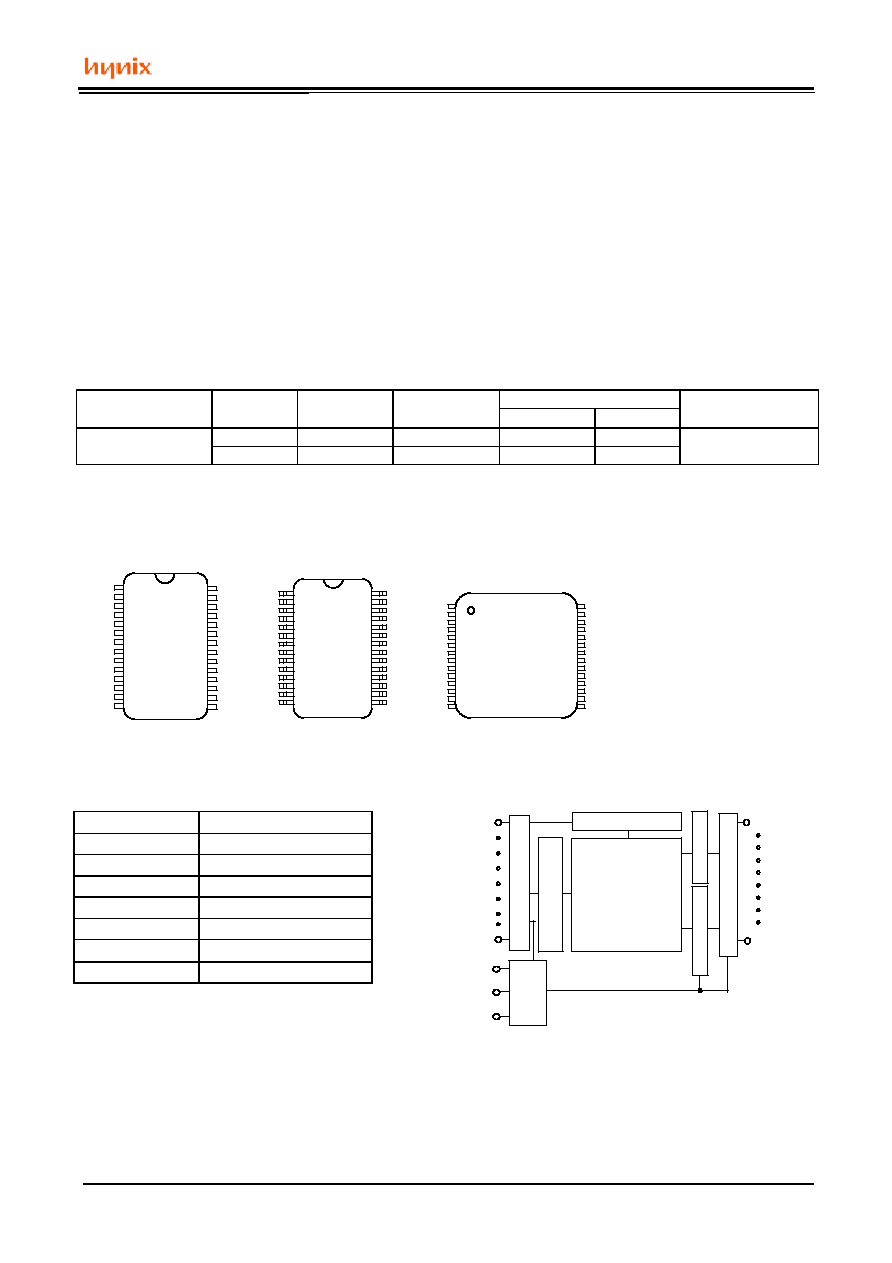
(Standard)
Product
Voltage
Speed
Operation
Standby Current(uA)
Temperature
No.
(V)
(ns)
Current(mA)
L
LL
(
�
C)
GM76C256CW
5.0
55/70
10
40
20
0~70(Normal)
3.0
120/150
2
20
10
Note 1. Current value is max.
PIN CONNECTION
1
2
3
4
5
6
7
8
9
10
11
12
13
14
28
27
26
25
24
23
22
21
20
19
18
17
16
15
Vcc
/WE
A8
A9
A11
/OE
A10
/CS
I/O8
I/O7
I/O6
I/O5
I/O4
A14
A12
A7
A6
A5
A4
A3
A2
A1
A0
I/O1
I/O2
I/O3
Vss
A13
1
2
3
4
5
6
7
8
9
10
11
12
13
14
28
27
26
25
24
23
22
21
20
19
18
17
16
15
Vcc
/WE
A8
A9
A11
/OE
A10
/CS
I/O8
I/O7
I/O6
I/O5
I/O4
A14
A12
A7
A6
A5
A4
A3
A2
A1
A0
I/O1
I/O2
I/O3
Vss
A13
1
2
3
4
5
6
7
8
9
10
11
12
13
14
28
27
26
25
24
23
22
21
20
19
18
17
16
15
A10
/CS
I/O7
I/O6
I/O5
I/O4
Vss
I/O3
I/O2
I/O1
A0
A1
A2
/OE
A11
A9
A8
A13
/WE
Vcc
A14
A12
A7
A6
A5
A4
A3
I/O8
PDIP SOP TSOP-I(Standard)
PIN DESCRIPTION BLOCK DIAGRAM
Pin Name
Pin Function
/CS
Chip Select
/WE
Write Enable
/OE
Output Enable
A0 ~ A14
Address Inputs
I/O1 ~ I/O8
Data Input/Output
Vcc
Power(
+
5.0V)
Vss
Ground
A14
COLUMN DECODER
A0
ROW DECODER
MEMORY ARRAY
512x512
SENSE AMP
OUTPUT BUFFER
I/O1
I/O8
ADD INPUT BUFFER
/CS
/OE
/WE
WRITE DRIVER
CONTROL
LOGIC

GM76C256CW Series
Rev 02 / Apr. 2001
2
ORDERING INFORMATION
Part No.
Speed
Power
Temp
Package
GM76C256CL-W
55/70
L-part
0 to 70
�
C
PDIP
GM76C256CLL-W
55/70
LL-part
0 to 70
�
C
PDIP
GM76C256CLFW-W
55/70
L-part
0 to 70
�
C
SOP
GM76C256CLLFW-W
55/70
LL-part
0 to 70
�
C
SOP
GM76C256CLT-W
55/70
L-part
0 to 70
�
C
TSOP-I Standard
GM76C256CLLT-W
55/70
LL-part
0 to 70
�
C
TSOP-I Standard
ABSOLUTE MAXIMUM RATING (1)
Symbol
Parameter
Rating
Unit
Vcc, V
IN,
V
OUT
Power Supply, Input/Output Voltage
-0.3 to 7.0
V
T
A
Operating Temperature
0 to 70
�
C
T
STG
Storage Temperature
-65 to 150
�
C
P
D
Power Dissipation
1.0
W
I
OUT
Data Output Current
50
mA
T
SOLDER
Lead Soldering Temperature & Time
260
�
10
�
C
�
sec
Note
1. Stresses greater than those listed under ABSOLUTE MAXIMUM RATINGS may cause permanent
damage to the device. This is stress rating only and the functional operation of the device under these or
any other conditions above those indicated in the operation of this specification is not implied.
Exposure to the absolute maximum rating conditions for extended period may affect reliability.
RECOMMENDED DC OPERATING CONDITIONS
Vcc = 5V
Vcc = 2.7 ~ 5.5V
Symbol
Parameter
Min.
Typ.
Max.
Min.
Typ.
Max.
Unit
Vcc
Power Supply Voltage
4.5
5.0
5.5
2.7
3.0
5.5
V
Vss
Ground
0
0
0
0
0
0
V
V
IH
Input High Voltage
2.2
-
Vcc+0.3
2.2
-
Vcc+0.3
V
V
IL
Input Low Voltage
-0.3
(1)
-
0.8
-0.3
(1)
-
0.4
V
Note
1. V
IL
= -3.0V for pulse width less than 50ns
TRUTH TABLE
/CS /WE /OE
Mode
I/O Operation
H
X
X Standby
High-Z
L
H
H Output Disabled High-Z
L
H
L Read
Data Out
L
L
X Write
Data In
Note
1. H=V
IH
, L=V
IL
, X=Don't Care
GM76C256CW Series
Rev 02 / Apr. 2001
3
DC CHARACTERISTICS
Vcc = 3V
�
10%,5V
�
10%, T
A
= 0
�
C
to 70
�
C
, unless otherwise specified.
Vcc = 3V
� �
10%
Vcc = 5V
� �
10%
Symbol
Parameter
Test Condition
Min Typ Max Min Typ Max
Unit
I
LI
Input Leakage Current
Vss < V
IN
< Vcc
-1
-
1
-1
-
1
uA
I
LO
Output Leakage Current Vss < V
OUT
< Vcc,
/CS = V
IH
or
/
OE
=
V
IH
or /WE = V
IL
-1
-
1
-1
-
1
uA
Icc
Operating Power Supply
Current
/CS = V
IL
,
V
IN
= V
IH
or V
IL,
I
I/O =
0mA
-
0.6
2
-
7 10
mA
/CS = V
IL,
I
I/O =
0mA,
Min. Duty Cycle = 100%,
V
IN
= V
IH
or V
IL
-
-
30
-
-
70
mA
I
CC1
Average Operating
Current
/CS = V
IL,
I
I/O =
0mA,
Cycle = 1us,
V
IN
= V
IH
or V
IL
-
-
5
-
-
10
mA
I
SB
TTL Standby Current
(TTL Inputs)
/CS= V
IH,
V
IN
= V
IH
or V
IL
-
-
0.3
-
-
1
mA
I
SB1
CMOS Standby Current /CS>Vcc-0.2V,
L
20
-
-
40
uA
(CMOS Inputs)
V
IN
>Vcc-0.2V or
V
IN
<Vss+0.2V
LL
10
-
-
20
uA
V
OL
Output Low Voltage
I
OL
= 2.1mA
0.4
-
-
0.4
V
V
OH
Output High Voltage
I
OH =
-1.0mA
2.2
2.4
-
-
V
Note : Typical values are at Vcc =3.0V/5.0V, T
A
= 25
�
C
AC CHARACTERISTICS(I)
Vcc = 3V
�
10%, T
A
= 0
�
C to 70
�
C (Normal) unless otherwise specified.
-55
-70
Min. Max. Min. Max.
1 tRC
Read Cycle Time
120
-
150
-
ns
2 tAA
Address Access Time
-
120
-
150
ns
3 tACS
Chip Select Access Time
-
120
-
150
ns
4 tOE
Output Enable to Output Valid
-
55
-
60
ns
5 tCLZ
Chip Select to Output in Low Z
10
-
10
-
ns
6 tOLZ
Output Enable to Output in Low Z
5
-
5
-
ns
7 tCHZ
Chip Disable to Output in High Z
0
40
0
50
ns
8 tOHZ
Out Disable to Output in High Z
0
40
0
50
ns
9 tOH
Output Hold from Address Change
10
-
10
-
ns
10 tWC
Write Cycle Time
120
-
150
-
ns
11 tCW
Chip Selection to End of Write
100
-
120
-
ns
12 tAW
Address Valid to End of Write
100
-
120
-
ns
13 tAS
Address Set-up Time
0
-
0
-
ns
14 tWP
Write Pulse Width
65
-
70
-
ns
15 tWR
Write Recovery Time
0
-
0
-
ns
16 tWHZ Write to Output in High Z
0
40
0
50
ns
17 tDW
Data to Write Time Overlap
40
-
50
-
ns
18 tDH
Data Hold from Write Time
0
-
0
-
ns
19 tOW
Output Active from End of Write
10
-
15
-
ns
READ CYCLE
WRITE CYCLE
Symbol
Parameter
#
Unit

GM76C256CW Series
Rev 02 / Apr. 2001
4
AC CHARACTERISTICS(II)
Vcc = 5V
�
10%, T
A
= 0
�
C to 70
�
C (Normal) unless otherwise specified.
-55
-70
Min. Max. Min. Max.
1 tRC
Read Cycle Time
55
-
70
-
ns
2 tAA
Address Access Time
-
55
-
70
ns
3 tACS
Chip Select Access Time
-
55
-
70
ns
4 tOE
Output Enable to Output Valid
-
30
-
35
ns
5 tCLZ
Chip Select to Output in Low Z
10
-
10
-
ns
6 tOLZ
Output Enable to Output in Low Z
5
-
5
-
ns
7 tCHZ
Chip Disable to Output in High Z
0
20
0
25
ns
8 tOHZ
Out Disable to Output in High Z
0
20
0
25
ns
9 tOH
Output Hold from Address Change
5
-
10
-
ns
10 tWC
Write Cycle Time
55
-
70
-
ns
11 tCW
Chip Selection to End of Write
50
-
65
-
ns
12 tAW
Address Valid to End of Write
50
-
60
-
ns
13 tAS
Address Set-up Time
0
-
0
-
ns
14 tWP
Write Pulse Width
45
-
50
-
ns
15 tWR
Write Recovery Time
0
-
0
-
ns
16 tWHZ Write to Output in High Z
0
20
0
25
ns
17 tDW
Data to Write Time Overlap
25
-
30
-
ns
18 tDH
Data Hold from Write Time
0
-
0
-
ns
19 tOW
Output Active from End of Write
5
-
5
-
ns
AC TEST CONDITIONS
T
A
= 0
�
C to 70
�
C (Normal) unless otherwise specified.
Parameter
Value
Input Pulse Level
5V
0.6V to 2.4V
3V
0.4V to 2.2V
Input Rise and Fall Time
5ns
Input and Output Timing Reference Level
1.5V
Output Load
tCLZ,tOLZ,tCHZ,tOHZ,tWHZ,tOW
CL = 5pF + 1TTL Load
Others
CL = 100pF + 1TTL Load
AC TEST LOADS
CL(1)
TTL
Note : Including jig and scope capacitance
CAPACITANCE
T
A
= 25
�
C, f = 1.0MHz
Symbol
Parameter
Condition
Max.
Unit
C
IN
Input Capacitance
V
IN
= 0V
6
pF
C
I/O
Input /Output Capacitance
V
I/O
= 0V
8
pF
Note : These parameters are sampled and not 100% tested
READ CYCLE
WRITE CYCLE
Symbol
Parameter
#
Unit
GM76C256CW Series
Rev 02 / Apr. 2001
5
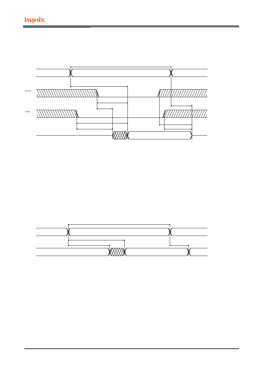
TIMING DIAGRAM
READ CYCLE 1
ADDR
OE
CS
Data
Out
Data Valid
tRC
tACS
tCLZ
tOE
tOLZ
tAA
tOH
tOHZ
tCHZ
High-Z
Note(READ CYCLE):
1. t
CHZ
and t
OHZ
are defined as the time at which the outputs achieve the open circuit conditions and arenot
referenced to output voltage levels.
2. At any given temperature and voltage condition, t
CHZ
max. is less than t
CLZ
min. both for a given device
and from device to device.
3. /WE is high for the read cycle.
READ CYCLE 2
tRC
tAA
Data Valid
Previous Data
tOH
tOH
ADDR
Data
Out
Note(READ CYCLE):
1. /WE is high for the read cycle.
2. Device is continuously selected /CS= V
IL.
3. /OE =V
IL
.
GM76C256CW Series
Rev 02 / Apr. 2001
6
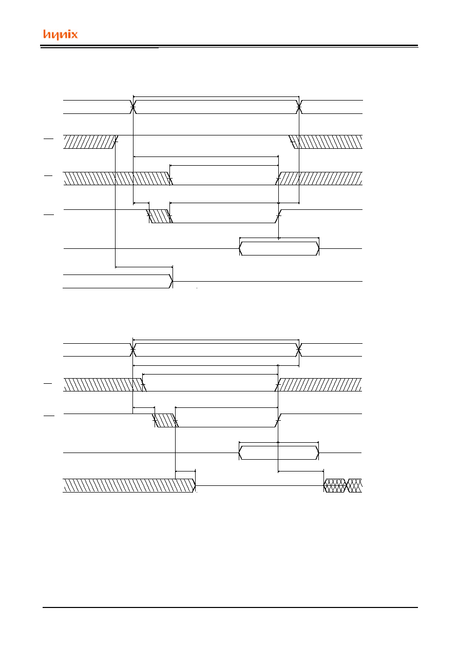
WRITE CYCLE 1(/OE Clocked)
ADDR
OE
CS
Data
Out
tWC
tDW
tOHZ
WE
Data Valid
tDH
tWP
tAS
Data In
tWR
tCW
tAW
WRITE CYCLE 2 (/OE Low Fixed)
tDW
tWHZ
WE
Data Valid
tDH
tWP
tAS
Data In
tWR
tCW
tAW
(7)
(8)
tOW
ADDR
CS
Data
Out
tWC
GM76C256CW Series
Rev 02 / Apr. 2001
7
Notes(WRITE CYCLE):
1. A write occurs during the overlap of a low /CS and a low /WE. A write begins at the latest transition
among /CS going low and /WE going low: A write ends at the earliest transition among /CS going high
and /WE going high. t
WP
is measured from the beginning of write to the end of write.
2. t
CW
is measured from the later of /CS going low to the end of write .
3. t
AS
is measured from the address valid to the beginning of write.
4. t
WR
is measured from the end of write to the address change. t
WR is
applied in case a write ends as /CS,
or /WE going high.
5. If /OE and /WE are in the read mode during this period, and the I/O pins are in the output low-Z state,
input of opposite phase of the output must not be applied because bus contention can occur.
6. If /CS goes low simultaneously with /WE going low, or after /WE going low, the outputs remain in high
impedance state.
7. D
OUT
is the same phase of the latest written data in this write cycle.
8. D
OUT
is the read data of the new address.
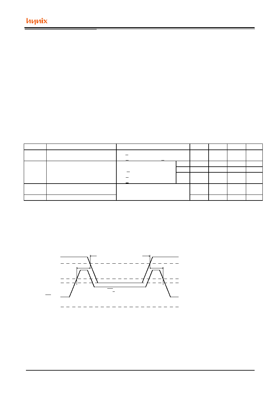
DATA RETENTION CHARACTERISTIC
Ta=0
�
C to 70
�
C (Normal)
Symbol
Parameter
Test Condition
Min
Typ
Max
Unit
V
DR
Vcc for Data Retention
CS>Vcc-0.2V,
2.0
-
-
V
V
IN
>Vcc-0.2V or V
IN
<Vss+0.2V
I
CCDR
Data Retention Current
Vcc=3.0V,
L
-
1
50
uA
/CS>Vcc-0.2V,
LL
-
0.5
10
uA
V
IN
>Vcc-0.2V or
V
IN
<Vss+0.2V
tCDR
Chip Deselect to Data
Retention Time
See Data Retention
0
-
-
ns
tR
Operating Recovery Time
Timing Diagram
tRC
(2)
-
-
ns
Notes
1. Typical values are under the condition of T
A
= 25
�
C.
2. tRC is read cycle time.
DATA RETENTION TIMING DIAGRAM
CS
VDR
CS>VCC-0.2V
tCDR
tR
VSS
VCC
4.5V
2.2V
DATA RETENTION MODE
GM76C256CW Series
Rev 02 / Apr. 2001
8
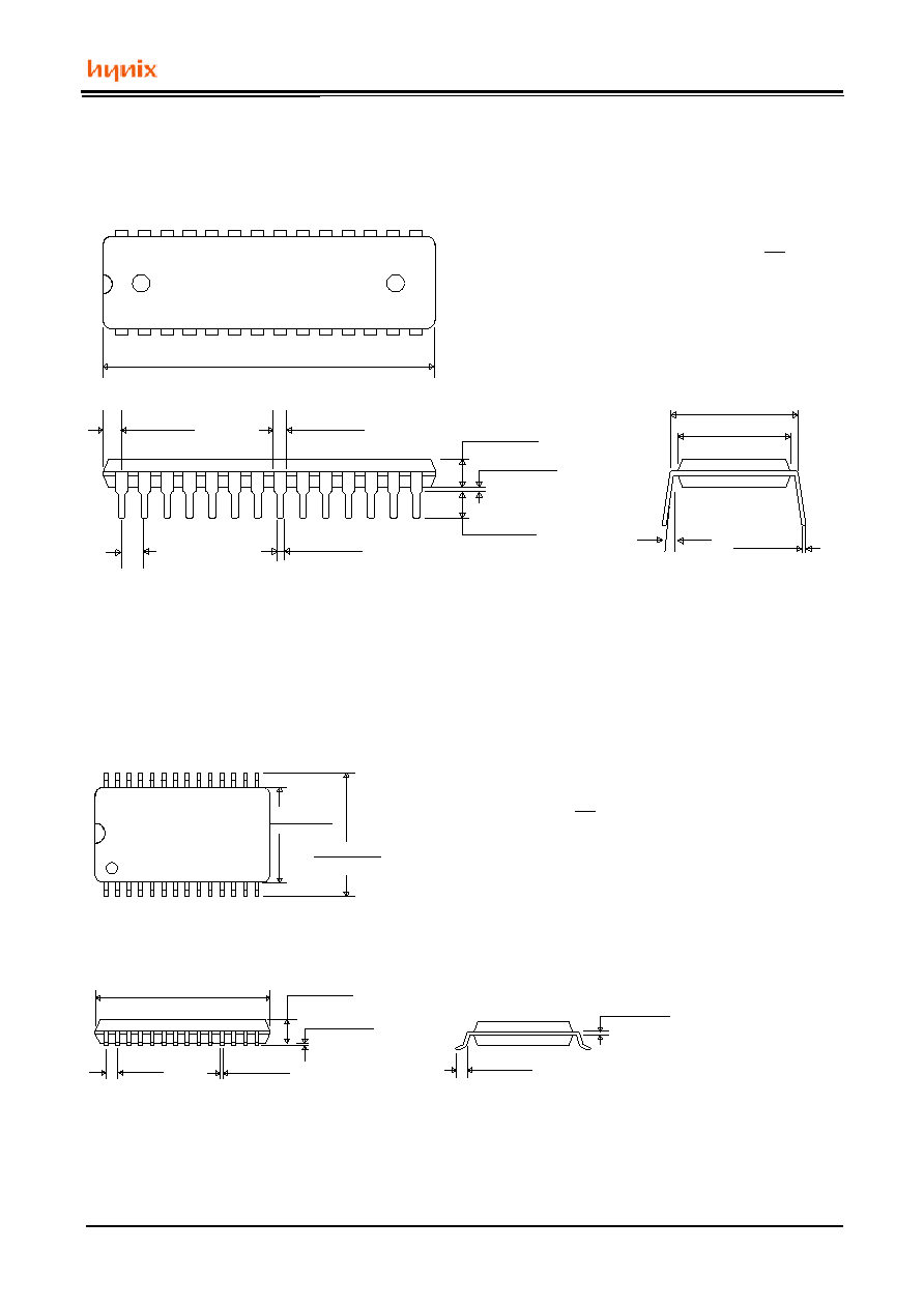
PACKAGE INFORMATION
28pin 600mil Dual In-Line Package(Blank)
�
UNIT : INCH(mm)
MIN.
MAX.
1.467(37.262)
1.447(36.754)
0.140(3.556)
0.120(3.048)
0.155(3.937)
0.145(3.683)
0.020(0.508)
0.021(0.533)
0.015(0.381)
0.100(2.54)BSC
0.065(1.650)
0.050(1.270)
0.090(2.286)
0.070(1.778)
0.014(0.356)
0.008(0.200)
0.600(15.240)BSC
0.550(13.970)
0.530(13.462)
0.035(0.889)
3 deg
11 deg
28pin 330mil Small O utline Package(FW)
UNIT : INCH(mm)
0.346(8.788)
0.338(8.585)
0.480(12.192)
0.460(11.684)
0.110(2.794)
0.094(2.388)
0.014(0.356)
0.002(0.051)
0.050(1.270)BSC
0.020(0.508)
0.014(0.356)
0.728(18.491)
0.720(18.288)
0.012(0.305)
0.008(0.203)
0.050(1.270)
0.030(0.762)
MAX
.
MIN.

GM76C256CW Series
Rev 02 / Apr. 2001
9
28pin 8x13.4mm Thin Small Outline Package Standard(T)
0.468(11.9)
0.460(11.7)
0.536(13.6)
0.520(13.2)
0.027(0.7)
0.012(0.3)
0.008(0.2)
0.004(0.1)
0.319(8.1)
0.311(7.9)
0.040(1.02)
0.036(0.91)
0.008(0.20)
0.002(0.05)
0.022(0.55 BSC)
UNIT : INCH(mm)
MAX.
MIN.

GM76C256CW Series
Rev 02 / Apr. 2001
10
MARKING INFORMATION
H
Y
U
N
D
A
I
G
M
7
6
C
2
5
6
C
c
c
-
s
s W
y
y
w
w
K
O
R
E
A
PDIP
Package
Marking Example
Index
� HYUNDAI
: Hynix Logo
� KOREA
: Origin Country
� GM76C256C
: Part Name
� cc
: Power Consumption
- L
: Low Power
- LL
: Low Low Power
� Blank / FW / T
: Package Type
- Blank
: DIP
- FW
: SOP
- T
: TSOP-I
� ss
: Speed
- 55
: 55ns
- 70
: 70ns
� W
: Wide Voltage
� yy
: Year ( ex : 00 = year 2000, 01 = year 2001 )
� ww
: Work Week ( ex : 12 = ww12 )
Note
- Capital Letter
: Fixed Item
- Small Letter
: Non-fixed Item
TSOP-I
SOP
H
Y
U
N
D
A
I
G
M
7
6
C
2
5
6
C
c
c
F
W s
s
y
y
w
w
K
O
R
E
A
W
H
Y
U
N
D
A
I
G
M
7
6
C
2
5
6
C
c
c
T
s
s W
y
y
w
w
K
O
R
E
A
H
Y
U
N
D
A
I
G
M
7
6
C
2
5
6
C
c
c
-
s
s W
y
y
w
w
K
O
R
E
A
PDIP
Package
Marking Example
Index
� HYUNDAI
: Hynix Logo
� KOREA
: Origin Country
� GM76C256C
: Part Name
� cc
: Power Consumption
- L
: Low Power
- LL
: Low Low Power
� Blank / FW / T
: Package Type
- Blank
: DIP
- FW
: SOP
- T
: TSOP-I
� ss
: Speed
- 55
: 55ns
- 70
: 70ns
� W
: Wide Voltage
� yy
: Year ( ex : 00 = year 2000, 01 = year 2001 )
� ww
: Work Week ( ex : 12 = ww12 )
Note
- Capital Letter
: Fixed Item
- Small Letter
: Non-fixed Item
TSOP-I
SOP
H
Y
U
N
D
A
I
G
M
7
6
C
2
5
6
C
c
c
F
W s
s
y
y
w
w
K
O
R
E
A
W
W
H
Y
U
N
D
A
I
G
M
7
6
C
2
5
6
C
c
c
T
s
s W
y
y
w
w
K
O
R
E
A
H
Y
U
N
D
A
I
G
M
7
6
C
2
5
6
C
c
c
T
s
s W
y
y
w
w
K
O
R
E
A