Äîêóìåíòàöèÿ è îïèñàíèÿ www.docs.chipfind.ru
Preliminary
Revision 1.0, November 2001
KEY FEATURES
n
Single Power Supply Operation
Read, program and erase operations from
2.7 to 3.6 volts
Ideal for battery-powered applications
n
High Performance
70 and 90 ns access time versions for full
voltage range operation
55 ns access time version for operation
from 3.0 to 3.6 volts
n
Ultra-low Power Consumption (Typical
Values)
Automatic sleep mode current: 0.2 µA
Standby mode current: 0.2 µA
Read current: 7 mA (at 5 Mhz)
Program/erase current: 15 mA
n
Flexible Sector Architecture:
One 16 KB, two 8 KB, one 32 KB and
fifteen 64 KB sectors in byte mode
One 8 KW, two 4 KW, one 16 KW and
fifteen 32 KW sectors in word mode
Top or bottom boot block configurations
available
n
Sector Protection
Allows locking of a sector or sectors to
prevent program or erase operations
within that sector
Sectors lockable in-system or via
programming equipment
Temporary Sector Unprotect allows
changes in locked sectors (requires high
voltage on RESET# pin)
n
Fast Program and Erase Times
Sector erase time: 0.5 sec typical for each
sector
Chip erase time: 10 sec typical
Byte program time: 9
µ
s typical
Word program time: 11
µ
s typical
n
Unlock Bypass Program Command
Reduces programming time when issuing
multiple program command sequences
n
Automatic Erase Algorithm Preprograms
and Erases Any Combination of Sectors
or the Entire Chip
n
Automatic Program Algorithm Writes and
Verifies Data at Specified Addresses
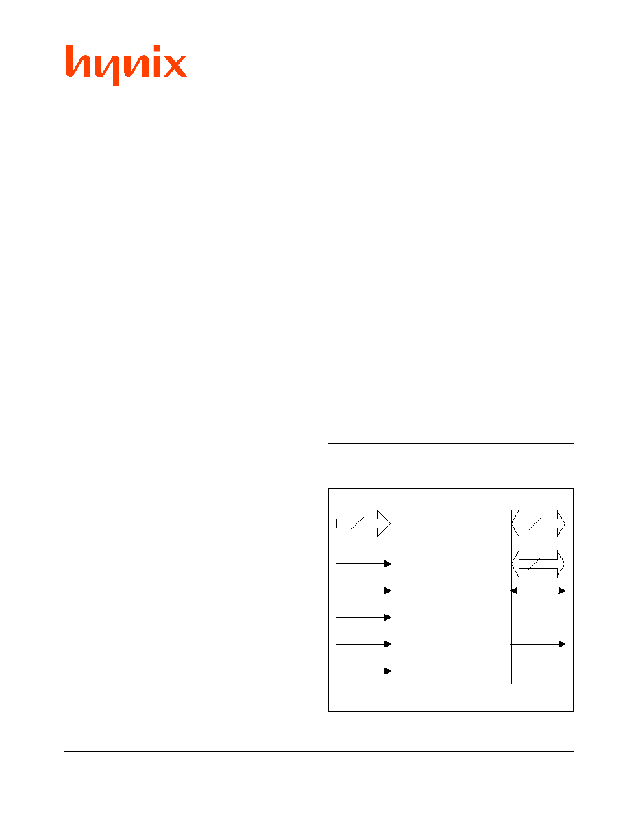
A[18:0]
19
C E #
O E #
R E S E T #
B Y T E #
W E #
8
7
DQ[7:0]
DQ[14:8]
DQ[15]/A[-1]
R Y / B Y #
LOGIC DIAGRAM
n
Minimum 100,000 Write Cycles per Sector
n
Compatible With JEDEC standards
Pinout and software compatible with
single-power supply Flash devices
Superior inadvertent write protection
n
Data# Polling and Toggle Bits
Provide software confirmation of
completion of program and erase
operations
n
Ready/Busy# Pin
Provides hardware confirmation of
completion of program and erase
operations
n
Erase Suspend/Erase Resume
Suspends an erase operation to allow
reading data from, or programming data
to, a sector that is not being erased
Erase Resume can then be invoked to
complete suspended erasure
n
Hardware Reset Pin (RESET#) Resets the
Device to Reading Array Data
n
Space Efficient Packaging
44-pin PSOP, 48-pin TSOP and 48-ball
FBGA packages
HY29LV800
8 Mbit (1M x 8/512K x 16) Low Voltage Flash Memory

2
Rev. 1.0/Nov. 01
HY29LV800
GENERAL DESCRIPTION
The HY29LV800 is an 8 Mbit, 3 volt-only, CMOS
Flash memory organized as 1,048,576 (1M) bytes
or 524,288 (512K) words that is available in 44-
pin PSOP, 48-pin TSOP and 48-ball FBGA pack-
ages. Word-wide data (x16) appears on DQ[15:0]
and byte-wide (x8) data appears on DQ[7:0].
The HY29LV800 can be programmed and erased
in-system with a single 3 volt V
CC
supply. Inter-
nally generated and regulated voltages are pro-
vided for program and erase operations, so that
the device does not require a higher voltage V
PP
power supply to perform those functions. The de-
vice can also be programmed in standard EPROM
programmers. Access times as low as 70 ns over
the full operating voltage range of 2.7 - 3.6 volts
are offered for timing compatibility with the zero
wait state requirements of high speed micropro-
cessors. A 55 ns version operating from 3.0 to
3.6 volts is also available. To eliminate bus con-
tention, the HY29LV800 has separate chip enable
(CE#), write enable (WE#) and output enable
(OE#) controls.
The device is compatible with the JEDEC single-
power-supply Flash command set standard. Com-
mands are written to the command register using
standard microprocessor write timings. They are
then routed to an internal state-machine that con-
trols the erase and programming circuits. Device
programming is performed a byte/word at a time
by executing the four-cycle Program Command
write sequence. This initiates an internal algorithm
that automatically times the program pulse widths
and verifies proper cell margin. Faster program-
ming times can be achieved by placing the
HY29LV800 in the Unlock Bypass mode, which
requires only two write cycles to program data in-
stead of four.
The HY29LV800's sector erase architecture allows
any number of array sectors to be erased and re-
programmed without affecting the data contents
of other sectors. Device erasure is initiated by
executing the Erase Command sequence. This
initiates an internal algorithm that automatically
preprograms the array (if it is not already pro-
grammed) before executing the erase operation.
As during programming cycles, the device auto-
matically times the erase pulse widths and veri-
fies proper cell margin. Hardware Sector Protec-
tion optionally disables both program and erase
operations in any combination of the sectors of
the memory array, while Temporary Sector Unpro-
tect allows in-system erasure and code changes
in previously protected sectors. Erase Suspend
enables the user to put erase on hold for any pe-
riod of time to read data from, or program data to,
any sector that is not selected for erasure. True
background erase can thus be achieved. The de-
vice is fully erased when shipped from the factory.
Addresses and data needed for the programming
and erase operations are internally latched during
write cycles, and the host system can detect
completion of a program or erase operation by
observing the RY/BY# pin, or by reading the DQ[7]
(Data# Polling) and DQ[6] (toggle) status bits.
Hardware data protection measures include a low
V
CC
detector that automatically inhibits write op-
erations during power transitions.
After a program or erase cycle has been com-
pleted, or after assertion of the RESET# pin (which
terminates any operation in progress), the device
is ready to read data or to accept another com-
mand. Reading data out of the device is similar to
reading from other Flash or EPROM devices.
Two power-saving features are embodied in the
HY29LV800. When addresses have been stable
for a specified amount of time, the device enters
the automatic sleep mode. The host can also place
the device into the standby mode. Power con-
sumption is greatly reduced in both these modes.
3
Rev. 1.0/Nov. 01
HY29LV800
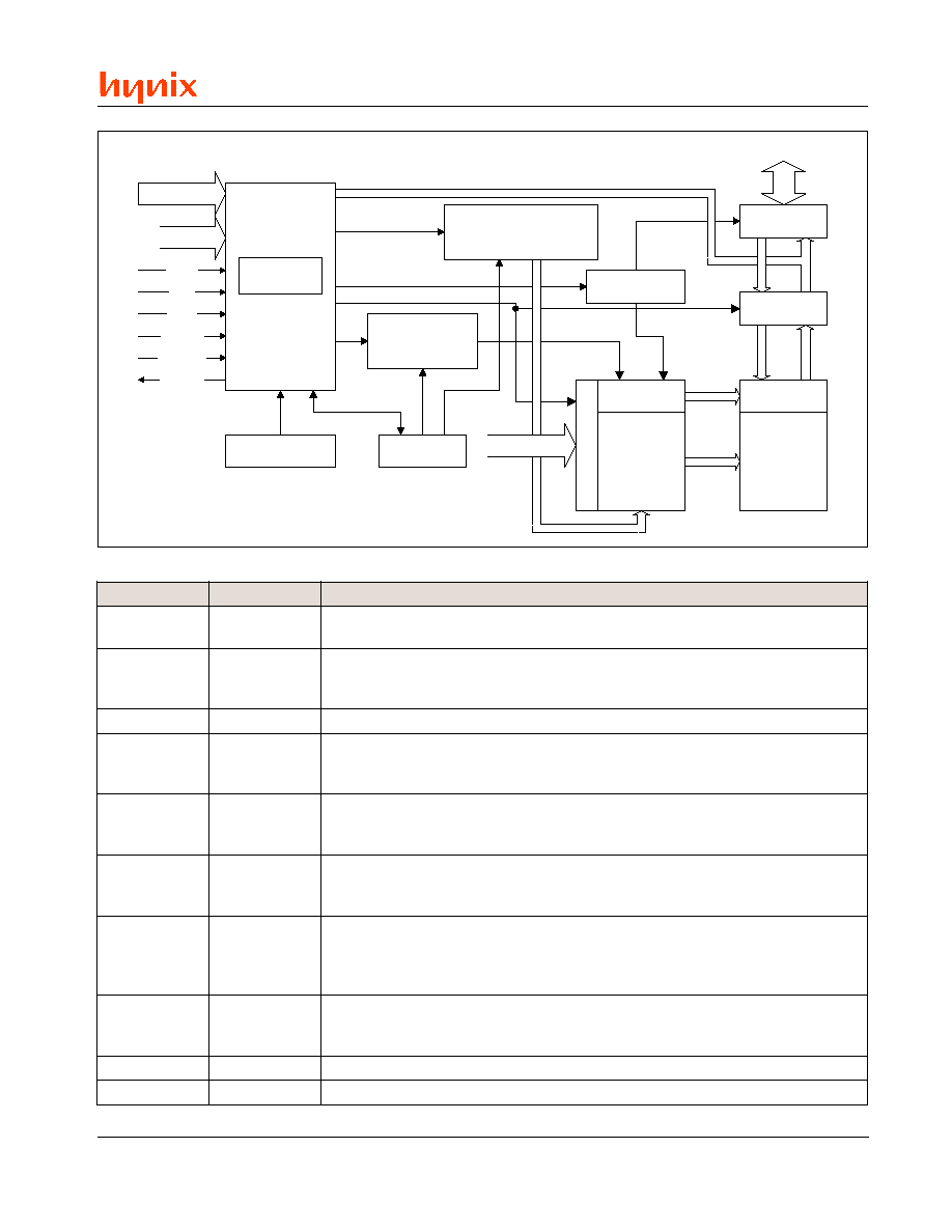
BLOCK DIAGRAM
STATE
C O N T R O L
W E #
C E #
OE#
BYTE#
C O M M A N D
R E G I S T E R
DQ[15:0]
A[18:0], A[-1]
V
C C
D E T E C T O R
T I M E R
E R A S E V O L T A G E
G E N E R A T O R A N D
S E C T O R S W I T C H E S
P R O G R A M
V O L T A G E
G E N E R A T O R
ADDRESS LATCH
X - D E C O D E R
Y - D E C O D E R
8 Mb FLASH
M E M O R Y
A R R A Y
(19 Sectors)
Y-GATING
D A T A L A T C H
I/O BUFFERS
I/O CONTROL
R E S E T #
DQ[15:0]
A[18:0], A[-1]
RY/BY#
SIGNAL DESCRIPTIONS
e
m
a
N
e
p
y
T
n
o
i
t
p
i
r
c
s
e
D
]
0
:
8
1
[
A
s
t
u
p
n
I
.
h
g
i
H
e
v
i
t
c
a
,
s
s
e
r
d
d
A
n
i
t
u
p
n
i
]
1
-
[
A
/
]
5
1
[
Q
D
e
h
t
h
t
i
w
d
e
n
i
b
m
o
c
,
s
t
u
p
n
i
9
1
e
s
e
h
T
.
s
n
o
it
a
r
e
p
o
e
t
i
r
w
r
o
d
a
e
r
r
o
f
y
a
r
r
a
e
h
t
n
i
h
t
i
w
n
o
it
a
c
o
l
e
n
o
t
c
e
l
e
s
,
e
d
o
m
e
t
y
B
,
]
1
-
[
A
/
]
5
1
[
Q
D
]
0
:
4
1
[
Q
D
s
t
u
p
t
u
O
/
s
t
u
p
n
I
e
t
a
t
s
-
i
r
T
h
g
i
H
e
v
i
t
c
a
,
s
u
B
a
t
a
D
d
a
e
r
r
o
f
h
t
a
p
a
t
a
d
t
i
b
-
6
1
r
o
-
8
n
a
e
d
i
v
o
r
p
s
n
i
p
e
s
e
h
T
.
t
i
b
0
2
e
h
t
f
o
B
S
L
e
h
t
s
a
d
e
s
u
s
i
]
1
-
[
A
/
]
5
1
[
Q
D
,
e
d
o
m
e
t
y
B
n
I
.
s
n
o
i
t
a
r
e
p
o
e
t
i
r
w
d
n
a
.
e
d
o
m
e
t
y
B
n
i
d
e
t
a
t
s
-
i
r
t
n
i
a
m
e
r
d
n
a
d
e
s
u
n
u
e
r
a
]
8
:
4
1
[
Q
D
.
t
u
p
n
i
s
s
e
r
d
d
a
e
t
y
b
#
E
T
Y
B
t
u
p
n
I
.
w
o
L
e
v
i
t
c
a
,
e
d
o
M
e
t
y
B
.
e
d
o
m
d
r
o
W
s
t
c
e
l
e
s
h
g
i
H
,
e
d
o
m
e
t
y
B
s
t
c
e
l
e
s
w
o
L
#
E
C
t
u
p
n
I
.
w
o
L
e
v
i
t
c
a
,
e
l
b
a
n
E
p
i
h
C
r
o
m
o
r
f
a
t
a
d
d
a
e
r
o
t
d
e
t
r
e
s
s
a
e
b
t
s
u
m
t
u
p
n
i
s
i
h
T
e
h
t
d
n
a
d
e
t
a
t
s
-
i
r
t
s
i
s
u
b
a
t
a
d
e
h
t
,
h
g
i
H
n
e
h
W
.
0
0
8
V
L
9
2
Y
H
e
h
t
o
t
a
t
a
d
e
t
i
r
w
.
e
d
o
m
y
b
d
n
a
t
S
e
h
t
n
i
d
e
c
a
l
p
s
i
e
c
i
v
e
d
#
E
O
t
u
p
n
I
w
o
L
e
v
i
t
c
a
,
e
l
b
a
n
E
t
u
p
t
u
O
r
o
f
d
e
t
a
g
e
n
d
n
a
s
n
o
i
t
a
r
e
p
o
d
a
e
r
r
o
f
d
e
t
r
e
s
s
A
.
e
h
t
g
n
i
r
u
d
d
a
e
r
s
i
d
r
o
w
a
r
o
e
t
y
b
a
r
e
h
t
e
h
w
s
e
n
i
m
r
e
t
e
d
#
E
T
Y
B
.
s
n
o
i
t
a
r
e
p
o
e
t
i
r
w
.
n
o
i
t
a
r
e
p
o
d
a
e
r
#
E
W
t
u
p
n
I
.
w
o
L
e
v
i
t
c
a
,
e
l
b
a
n
E
e
t
i
r
W
d
n
a
m
m
o
c
r
o
s
d
n
a
m
m
o
c
f
o
g
n
i
t
i
r
w
s
l
o
r
t
n
o
C
e
t
i
r
w
A
.
y
a
r
r
a
y
r
o
m
e
m
e
h
t
f
o
s
r
o
t
c
e
s
e
s
a
r
e
r
o
a
t
a
d
m
a
r
g
o
r
p
o
t
r
e
d
r
o
n
i
s
e
c
n
e
u
q
e
s
h
g
i
H
s
i
#
E
O
d
n
a
w
o
L
s
i
#
E
C
e
li
h
w
d
e
t
r
e
s
s
a
s
i
#
E
W
n
e
h
w
e
c
a
l
p
s
e
k
a
t
n
o
it
a
r
e
p
o
.
#
T
E
S
E
R
t
u
p
n
I
.
w
o
L
e
v
i
t
c
a
,
t
e
s
e
R
e
r
a
w
d
r
a
H
e
h
t
g
n
i
t
t
e
s
e
r
f
o
d
o
h
t
e
m
e
r
a
w
d
r
a
h
a
s
e
d
i
v
o
r
P
y
l
e
t
a
i
d
e
m
m
i
t
i
,
t
e
s
e
r
s
i
e
c
i
v
e
d
e
h
t
n
e
h
W
.
e
t
a
t
s
y
a
r
r
a
d
a
e
r
e
h
t
o
t
0
0
8
V
L
9
2
Y
H
e
c
i
v
e
d
e
h
t
,
d
e
t
r
e
s
s
a
s
i
#
T
E
S
E
R
e
l
i
h
W
.
s
s
e
r
g
o
r
p
n
i
n
o
i
t
a
r
e
p
o
y
n
a
s
e
t
a
n
i
m
r
e
t
.
e
d
o
m
y
b
d
n
a
t
S
e
h
t
n
i
e
b
ll
i
w
#
Y
B
/
Y
R
t
u
p
t
u
O
n
i
a
r
D
n
e
p
O
.
s
u
t
a
t
S
y
s
u
B
/
y
d
a
e
R
n
i
s
i
d
n
a
m
m
o
c
e
s
a
r
e
r
o
e
t
i
r
w
a
r
e
h
t
e
h
w
s
e
t
a
c
i
d
n
I
y
l
e
v
i
t
c
a
s
i
e
c
i
v
e
d
e
h
t
e
l
i
h
w
w
o
L
s
n
i
a
m
e
R
.
d
e
t
e
l
p
m
o
c
n
e
e
b
s
a
h
r
o
s
s
e
r
g
o
r
p
.
a
t
a
d
y
a
r
r
a
d
a
e
r
o
t
y
d
a
e
r
s
i
t
i
n
e
h
w
h
g
i
H
s
e
o
g
d
n
a
,
g
n
i
s
a
r
e
r
o
a
t
a
d
g
n
i
m
m
a
r
g
o
r
p
V
C
C
-
-
.
y
l
p
p
u
s
r
e
w
o
p
)
l
a
n
i
m
o
n
(
t
l
o
v
-
3
V
S
S
-
-
.
d
n
u
o
r
g
l
a
n
g
i
s
d
n
a
r
e
w
o
P
4
Rev. 1.0/Nov. 01
HY29LV800
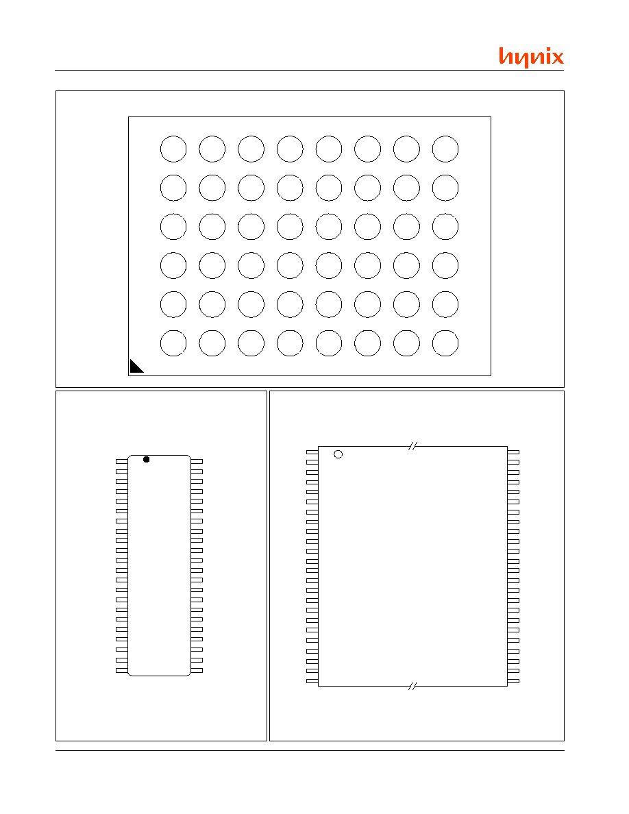
PIN CONFIGURATIONS
A 6
B 6
C 6
D 6
E 6
F 6
G 6
H 6
A 5
B 5
C 5
D 5
E 5
F 5
G 5
H 5
A 4
B 4
C 4
D 4
E 4
F 4
G 4
H 4
A 3
B 3
C 3
D 3
E 3
F 3
G 3
H 3
A 2
B 2
C 2
D 2
E 2
F 2
G 2
H 2
A 1
B 1
C 1
D 1
E 1
F 1
G 1
H 1
A[13]
A[12]
A[14]
A[15]
A[16]
BYTE#
DQ[15]/A[-1]
V
S S
A[9]
A[8]
A[10]
A[11]
DQ[7]
DQ[14]
DQ[13]
DQ[6]
W E #
R E S E T #
N C
N C
DQ[5]
DQ[12]
V
C C
DQ[4]
RY/BY#
N C
A[18]
N C
DQ[2]
DQ[10]
DQ[11]
DQ[3]
A[7]
A[17]
A[6]
A[5]
DQ[0]
DQ[8]
DQ[9]
DQ[1]
A[3]
A[4]
A[2]
A[1]
A[0]
C E #
O E #
V
S S
48-Ball FBGA (6 x 8 mm, Top View, Balls Facing Down)
Standard
TSOP48
D Q 7
D Q 1 4
4 4
4 3
D Q 6
D Q 1 3
4 2
4 1
D Q 5
D Q 1 2
4 0
3 9
D Q 4
V
C C
3 8
3 7
D Q 1 1
D Q 3
3 6
3 5
D Q 1 0
D Q 2
3 4
3 3
D Q 9
D Q 1
3 2
3 1
D Q 8
D Q 0
3 0
2 9
A 1 6
B Y T E #
4 8
4 7
V
S S
D Q 1 5 / A - 1
4 6
4 5
O E #
V
S S
2 8
2 7
C E #
A 0
2 6
2 5
A 1 1
A 1 0
5
6
A 9
A 8
7
8
N C
N C
9
1 0
W E #
R E S E T #
1 1
1 2
N C
N C
1 3
1 4
R Y / B Y #
A 1 8
1 5
1 6
A 1 7
A 7
1 7
1 8
A 6
A 5
1 9
2 0
A 1 5
A 1 4
1
2
A 1 3
A 1 2
3
4
A 4
A 3
2 1
2 2
A 2
A 1
2 3
2 4
A 6
A 5
5
6
A 4
A 3
7
8
A 2
A 1
9
1 0
A 0
C E #
1 1
1 2
V
S S
O E #
1 3
1 4
D Q 0
D Q 8
1 5
1 6
D Q 1
D Q 9
1 7
1 8
D Q 2
D Q 1 0
1 9
2 0
D Q 3
D Q 1 1
2 1
2 2
R Y / B Y #
A 1 8
1
2
A 1 7
A 7
3
4
A 1 0
A 1 1
4 0
3 9
A 1 2
A 1 3
3 8
3 7
A 1 4
A 1 5
3 6
3 5
A 1 6
B Y T E #
3 4
3 3
V
S S
D Q 1 5 / A - 1
3 2
3 1
D Q 7
D Q 1 4
3 0
2 9
D Q 6
D Q 1 3
2 8
2 7
D Q 5
D Q 1 2
2 6
2 5
D Q 4
V
C C
2 4
2 3
R E S E T #
W E #
4 4
4 3
A 8
A 9
4 2
4 1
PSOP44

5
Rev. 1.0/Nov. 01
HY29LV800
CONVENTIONS
Unless otherwise noted, a positive logic (active
High) convention is assumed throughout this docu-
ment, whereby the presence at a pin of a higher,
more positive voltage (V
IH
) causes assertion of the
signal. A `#' symbol following the signal name, e.g.,
RESET#, indicates that the signal is asserted in
the Low state (V
IL
). See DC specifications for V
IH
and V
IL
values.
Whenever a signal is separated into numbered
bits, e.g., DQ[7], DQ[6], ..., DQ[0], the family of
bits may also be shown collectively, e.g., as
DQ[7:0].
The designation 0xNNNN (N = 0, 1, 2, . . . , 9, A, .
. . , E, F) indicates a number expressed in hexadeci-
mal notation. The designation 0bXXXX indicates a
number expressed in binary notation (X = 0, 1).
MEMORY ARRAY ORGANIZATION
The 8 Mbit Flash memory array is organized into
19 blocks called sectors (S0, S1, . . . , S18). A
sector is the smallest unit that can be erased and
that can be protected to prevent accidental or un-
authorized erasure. See the `Bus Operations' and
`Command Definitions' sections of this document
for additional information on these functions.
In the HY29LV800, four of the sectors, which com-
prise the boot block, vary in size from 8 to 32
Kbytes (4 to 16 Kwords), while the remaining 15
sectors are uniformly sized at 64 Kbytes (32
Kwords). The boot block can be located at the
bottom of the address range (HY29LV800B) or at
the top of the address range (HY29LV800T).
Tables 1 and 2 define the sector addresses and
corresponding address ranges for the top and bot-
tom boot block versions of the HY29LV800.
BUS OPERATIONS
Device bus operations are initiated through the
internal command register, which consists of sets
of latches that store the commands, along with
the address and data information, if any, needed
to execute the specific command. The command
register itself does not occupy any addressable
memory location. The contents of the command
register serve as inputs to an internal state ma-
chine whose outputs control the operation of the
device. Table 3 lists the normal bus operations,
the inputs and control levels they require, and the
resulting outputs. Certain bus operations require
a high voltage on one or more device pins. Those
are described in Table 4.
Read Operation
Data is read from the HY29LV800 by using stan-
dard microprocessor read cycles while placing the
byte or word address on the device's address in-
puts. The host system must drive the CE# and
OE# pins LOW and drive WE# high for a valid read
operation to take place. The BYTE# pin determines
whether the device outputs array data in words
(DQ[15:0]) or in bytes (DQ[7:0]).
The HY29LV800 is automatically set for reading
array data after device power-up and after a hard-
ware reset to ensure that no spurious alteration of
the memory content occurs during the power tran-
sition. No command is necessary in this mode to
obtain array data, and the device remains enabled
for read accesses until the command register con-
tents are altered.
This device features an Erase Suspend mode.
While in this mode, the host may read the array
data from any sector of memory that is not marked
for erasure. If the host reads from an address
within an erase-suspended (or erasing) sector, or
while the device is performing a byte or word pro-
gram operation, the device outputs status data
instead of array data. After completing an Auto-
matic Program or Automatic Erase algorithm within
a sector, that sector automatically returns to the
read array data mode. After completing a program-
ming operation in the Erase Suspend mode, the
system may once again read array data with the
same exception noted above.
The host must issue a hardware reset or the soft-
ware reset command to return a sector to the read
array data mode if DQ[5] goes high during a pro-
gram or erase cycle, or to return the device to the
read array data mode while it is in the Electronic
ID mode.