Document Outline
- Revision History
- DESCRIPTION
- FEATURES
- ORDERING INFORMATION
- PIN ASSIGNMENTS
- PIN DESCRIPTION
- FUNCTIONAL BLOCK DIAGRAM
- BASIC FUNCTIONAL DESCRIPTION
- ABSOLUTE MAXIMUM RATING
- DC OPERATING CONDITION
- AC OPERATING TEST CONDITION
- CAPACITANCE
- DC CHARACTERISTICS I
- DC CHARACTERISTICS II
- AC CHARACTERISTICS I
- AC CHARACTERISTICS II
- COMMAND TRUTH TABLE
- Untitled
This document is a general product description and is subject to change without notice. Hynix does not assume any responsibility for
use of circuits described. No patent licenses are implied.
Rev. 1.1 / Jan. 2005
1
128Mb Synchronous DRAM based on 2M x 4Bank x16 I/O
Document Title
4Bank x 2M x 16bits Synchronous DRAM
Revision History
Revision No.
History
Draft Date
Remark
1.0
First Version Release
Dec. 2004
1.1
1. Corrected PIN ASSIGNMENT A12 to NC
Jan. 2005
Rev. 1.1 / Jan. 2005
2
Synchronous DRAM Memory 128Mbit (8Mx16bit)
HY57V281620E(L)T(P) Series
DESCRIPTION
The Hynix HY57V281620E(L)T(P) series is a 134,217,728bit CMOS Synchronous DRAM, ideally suited for the memory
applications which require wide data I/O and high bandwidth. HY57V281620E(L)T(P) series is organized as 4banks of
2,097,152 x 16.
HY57V281620E(L)T(P) is offering fully synchronous operation referenced to a positive edge of the clock. All inputs and
outputs are synchronized with the rising edge of the clock input. The data paths are internally pipelined to achieve
very high bandwidth. All input and output voltage levels are compatible with LVTTL.
Programmable options include the length of pipeline (Read latency of 2 or 3), the number of consecutive read or write
cycles initiated by a single control command (Burst length of 1,2,4,8 or full page), and the burst count sequence(se-
quential or interleave). A burst of read or write cycles in progress can be terminated by a burst terminate command or
can be interrupted and replaced by a new burst read or write command on any cycle. (This pipelined design is not re-
stricted by a '2N' rule)
FEATURES
ORDERING INFORMATION
Note:
1. HY57V281620ET Series: Normal power, Leaded.
2. HY57V281620ELT Series: Low power, Leaded.
3. HY57V281620ETP Series: Normal power, Lead Free.
4. HY57V281620ELTP Series: Low power, Lead Free.
Part No.
Clock Frequency
Organization
Interface
Package
HY57V281620E(L)T(P)-5
200MHz
4Banks x 2Mbits x16
LVTTL
54 Pin TSOPII
HY57V281620E(L)T(P)-6
166MHz
HY57V281620E(L)T(P)-7
143MHz
HY57V281620E(L)T(P)-H
133MHz
�
Voltage: VDD, VDDQ 3.3V supply voltage
�
All device pins are compatible with LVTTL interface
� 54 Pin TSOPII (Lead or Lead Free Package)
�
All inputs and outputs referenced to positive edge of
system clock
�
Data mask function by UDQM, LDQM
�
Internal four banks operation
�
Auto refresh and self refresh
�
4096 Refresh cycles / 64ms
�
Programmable Burst Length and Burst Type
- 1, 2, 4, 8 or full page for Sequential Burst
- 1, 2, 4 or 8 for Interleave Burst
�
Programmable CAS Latency; 2, 3 Clocks
�
Burst Read Single Write operation
Rev. 1.1 / Jan. 2005
3
Synchronous DRAM Memory 128Mbit (8Mx16bit)
HY57V281620E(L)T(P) Series
PIN ASSIGNMENTS
VDD
DQ0
VDDQ
DQ1
DQ2
VSSQ
DQ3
DQ4
VDDQ
DQ5
DQ6
VSSQ
DQ7
VDD
LDQM
/WE
/CAS
/RAS
/CS
BA0
BA1
A10/AP
A0
A1
A2
A3
VDD
1
2
3
4
5
6
7
8
9
10
11
12
13
14
15
16
17
18
19
20
21
22
23
24
25
26
27
VSS
DQ15
VSSQ
DQ14
DQ13
VDDQ
DQ12
DQ11
VSSQ
DQ10
DQ9
VDDQ
DQ8
VSS
NC
UDQM
CLK
CKE
NC
A11
A9
A8
A7
A6
A5
A4
VSS
54
53
52
51
50
49
48
47
46
45
44
43
42
41
40
39
38
37
36
35
34
33
32
31
30
29
28
54 Pin TSOPII
400mil x 875mil
0.8mm pin pitch
Rev. 1.1 / Jan. 2005
4
Synchronous DRAM Memory 128Mbit (8Mx16bit)
HY57V281620E(L)T(P) Series
PIN DESCRIPTION
SYMBOL
TYPE
DESCRIPTION
CLK
Clock
The system clock input. All other inputs are registered to the SDRAM
on the rising edge of CLK
CKE
Clock Enable
Controls internal clock signal and when deactivated, the SDRAM will
be one of the states among power down, suspend or self refresh
CS
Chip Select
Enables or disables all inputs except CLK, CKE, UDQM and LDQM
BA0, BA1
Bank Address
Selects bank to be activated during RAS activity
Selects bank to be read/written during CAS activity
A0 ~ A11
Address
Row Address: RA0 ~ RA11, Column Address: CA0 ~ CA8
Auto-precharge flag: A10
RAS, CAS, WE
Row Address Strobe,
Column Address Strobe,
Write Enable
RAS, CAS and WE define the operation
Refer function truth table for details
UDQM, LDQM
Data Input/Output Mask
Controls output buffers in read mode and masks input data in write
mode
DQ0 ~ DQ15
Data Input/Output
Multiplexed data input / output pin
VDD/VSS
Power Supply/Ground
Power supply for internal circuits and input buffers
VDDQ/VSSQ
Data Output Power/Ground Power supply for output buffers
NC
No Connection
No connection
Rev. 1.1 / Jan. 2005
5
Synchronous DRAM Memory 128Mbit (8Mx16bit)
HY57V281620E(L)T(P) Series
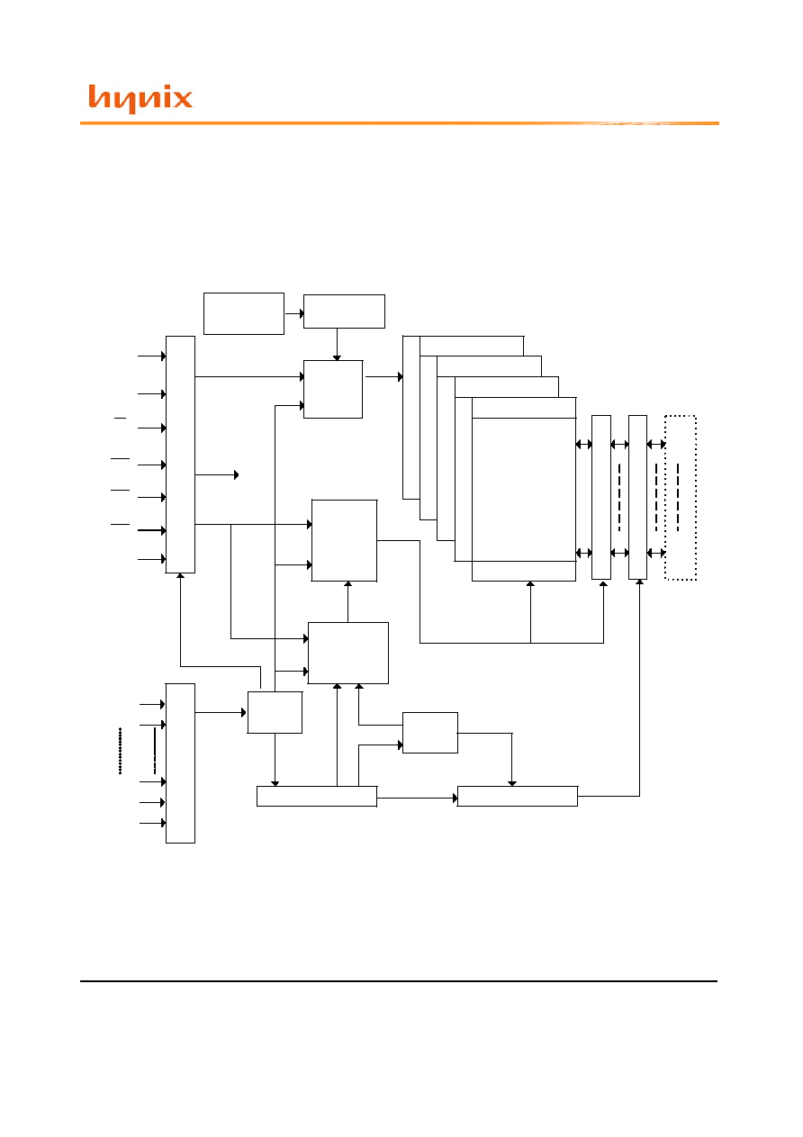
FUNCTIONAL BLOCK DIAGRAM
2Mbit x 4banks x 16 I/O Synchronous DRAM
Internal Row
Counter
Column
Pre
Decoder
Column Add
Counter
Self refresh
logic & timer
Sen
s
e
A
M
P
& I
/
O
Gate
I/O
Buf
f
er & L
o
gic
Address
Register
Burst
Counter
Mode Register
S
t
a
t
e M
a
c
h
i
n
e
A
d
d
r
e
s
s B
u
f
f
er
s
Bank Select
Column
Active
Row Active
CAS Latency
CLK
CKE
CS
RAS
CAS
WE
U/LDQM
A0
A1
BA1
BA0
A11
Row
Pre
Decoder
Refresh
DQ0
DQ15
X-D
e
c
o
der
X-D
e
c
o
der
X-D
e
coder
X-
De
co
d
e
r
Y-Decoder
2Mx16 BANK 0
2Mx16 BANK 1
2Mx16 BANK 2
2Mx16 BANK 3
Memory
Cell
Array
Data Out Control
Pipe Line
Control
Rev. 1.1 / Jan. 2005
6
Synchronous DRAM Memory 128Mbit (8Mx16bit)
HY57V281620E(L)T(P) Series
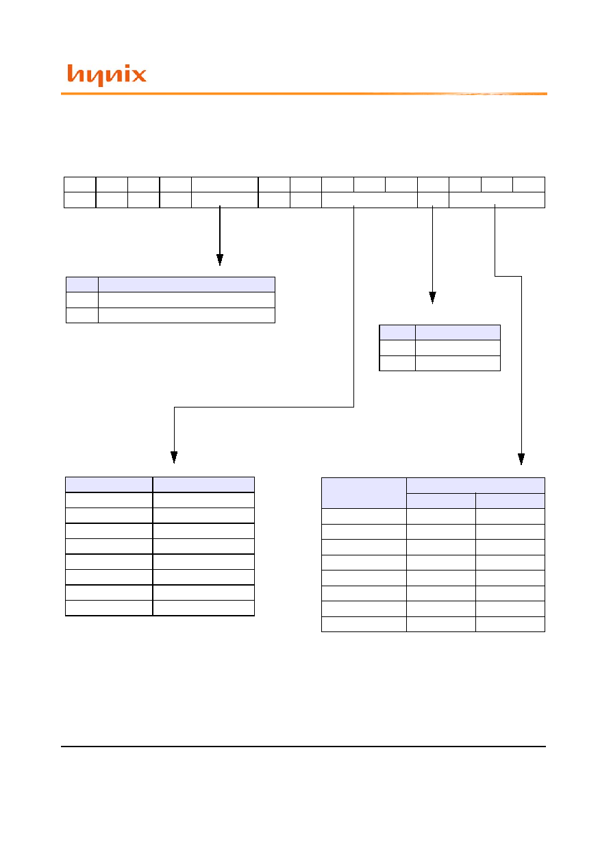
BASIC FUNCTIONAL DESCRIPTION
Mode Register
BA1
BA0
A11
A10
A9
A8
A7
A6
A5
A4
A3
A2
A1
A0
0
0
0
0
OP Code
0
0
CAS Latency
BT
Burst Length
OP Code
A9
Write Mode
0
Burst Read and Burst Write
1
Burst Read and Single Write
Burst Type
A3
Burst Type
0
Sequential
1
Interleave
Burst Length
A2
A1
A0
Burst Length
A3 = 0
A3=1
0
0
0
1
1
0
0
1
2
2
0
1
0
4
4
0
1
1
8
8
1
0
0
Reserved
Reserved
1
0
1
Reserved
Reserved
1
1
0
Reserved
Reserved
1
1
1
Full Page
Reserved
CAS Latency
A6
A5
A4
CAS Latency
0
0
0
Reserved
0
0
1
1
0
1
0
2
0
1
1
3
1
0
0
Reserved
1
0
1
Reserved
1
1
0
Reserved
1
1
1
Reserved
Rev. 1.1 / Jan. 2005
7
Synchronous DRAM Memory 128Mbit (8Mx16bit)
HY57V281620E(L)T(P) Series
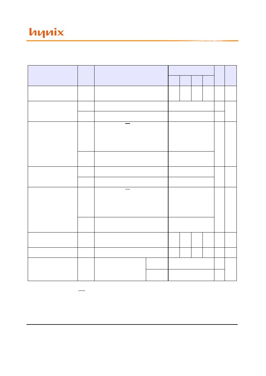
ABSOLUTE MAXIMUM RATING
DC OPERATING CONDITION
(T
A
= 0 to 70
o
C
)
Note: 1. All voltages are referenced to V
SS
= 0V
2. V
IH
(max) is acceptable 5.6V AC pulse width with <=3ns of duration.
3. V
IL
(min) is acceptable -2.0V AC pulse width with <=3ns of duration
AC OPERATING TEST CONDITION
(T
A
= 0 to 70
o
C
, V
DD
=3.3
�0.3V, V
SS
=0V)
Note 1.
Parameter
Symbol
Rating
Unit
Ambient Temperature
TA
0 ~ 70
o
C
Storage Temperature
TSTG
-55 ~ 125
o
C
Voltage on Any Pin relative to VSS
VIN, VOUT
-1.0 ~ 4.6
V
Voltage on VDD relative to VSS
VDD, VDDQ
-1.0 ~ 4.6
V
Short Circuit Output Current
IOS
50
mA
Power Dissipation
PD
1
W
Soldering Temperature / Time
TSOLDER
260 / 10
o
C / Sec
Parameter
Symbol
Min.
Typ
Max
Unit
Note
Power Supply Voltage
V
DD,
V
DDQ
3.0
3.3
3.6
V
1
Input High Voltage
V
IH
2.0
3.0
V
DDQ +
0.3
V
1, 2
Input Low Voltage
V
IL
-0.3
-
0.8
V
1, 3
Parameter
Symbol
Value
Unit
Note
AC Input High / Low Level Voltage
V
IH
/ V
IL
2.4 / 0.4
V
Input Timing Measurement Reference Level Voltage
V
trip
1.4
V
Input Rise / Fall Time
t
R
/ t
F
1
ns
Output Timing Measurement Reference Level Voltage
V
outref
1.4
V
Output Load Capacitance for Access Time Measurement
CL
50
pF
1
Z0 = 50
Output
Output
Vtt = 1.4V
50pF
RT = 50
Vtt = 1.4V
50pF
DC Output Load Circuit
AC Output Load Circuit
RT = 500
Rev. 1.1 / Jan. 2005
8
Synchronous DRAM Memory 128Mbit (8Mx16bit)
HY57V281620E(L)T(P) Series
CAPACITANCE
(T
A
= 0 to 70
o
C
, f=1MHz, V
DD
=3.3V)
DC CHARACTERISTICS I
(T
A
= 0 to 70
o
C
)
Note:
1. V
IN
= 0 to 3.3V, All other balls are not tested under V
IN
=0V
2. D
OUT
is disabled, V
OUT
=0 to 3.6
Parameter
Pin
Symbol
Min
Max
Unit
Input capacitance
CLK
CI1
2.0
4.0
pF
A0 ~ A11, BA0, BA1, CKE, CS, RAS, CAS,
WE, LDQM, UDQM
CI2
2.5
5.0
pF
Data input / output capacitance
DQ0 ~ DQ15
CI/O
3.0
5.5
pF
Parameter
Symbol
Min
Max
Unit
Note
Input Leakage Current
I
LI
-1
1
uA
1
Output Leakage Current
I
LO
-1
1
uA
2
Output High Voltage
V
OH
2.4
-
V
IOH = -2mA
Output Low Voltage
V
OL
-
0.4
V
IOL = +2mA
Rev. 1.1 / Jan. 2005
9
Synchronous DRAM Memory 128Mbit (8Mx16bit)
HY57V281620E(L)T(P) Series
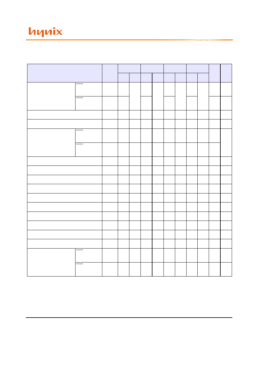
DC CHARACTERISTICS II
(T
A
= 0 to 70
o
C
)
Note: 1. I
DD1
and I
DD4
depend on output loading and cycle rates. Specified values are measured with the output open
2. Min. of tRRC (Refresh RAS cycle time) is shown at AC CHARACTERISTICS II
3. HY57V281620ET(P) Series: Normal Power
HY57V281620ELT(P) Series: Low Power
Parameter
Sym-
bol
Test Condition
Speed
Unit Note
5
6
7
H
Operating Current
I
DD1
Burst length=1, One bank active
t
RC
t
RC
(min), I
OL
=0mA
120
110
100
100 mA
1
Precharge Standby Current
in Power Down Mode
I
DD2P
CKE
V
IL
(max), t
CK
= 15ns
2
mA
I
DD2PS
CKE
V
IL
(max), t
CK
=
2
mA
Precharge Standby Current
in Non Power Down Mode
I
DD2N
CKE
V
IH
(min), CS
V
IH
(min), t
CK
=
15ns
Input signals are changed one time dur-
ing 2clks.
All other pins
V
DD
-0.2V or
0.2V
18
mA
I
DD2NS
CKE
V
IH
(min), t
CK
=
Input signals are stable.
15
Active Standby Current
in Power Down Mode
I
DD3P
CKE
V
IL
(max), t
CK
= 15ns
3
mA
I
DD3PS
CKE
V
IL
(max), t
CK
=
3
Active Standby Current
in Non Power Down Mode
I
DD3N
CKE
V
IH
(min), CS
V
IH
(min), t
CK
=
15ns
Input signals are changed one time dur-
ing 2clks.
All other pins
V
DD
-0.2V or
0.2V
40
mA
I
DD3NS
CKE
V
IH
(min), t
CK
=
Input signals are stable.
35
Burst Mode Operating Cur-
rent
I
DD4
t
CK
t
CK
(min), I
OL
=0mA
All banks active
120
110
100
100 mA
1
Auto Refresh Current
I
DD5
t
RC
t
RC
(min), All banks active
210
200
190
190 mA
2
Self Refresh Current
I
DD6
CKE
0.2V
Normal
2
mA
3
Low power
800
uA
Rev. 1.1 / Jan. 2005
10
Synchronous DRAM Memory 128Mbit (8Mx16bit)
HY57V281620E(L)T(P) Series
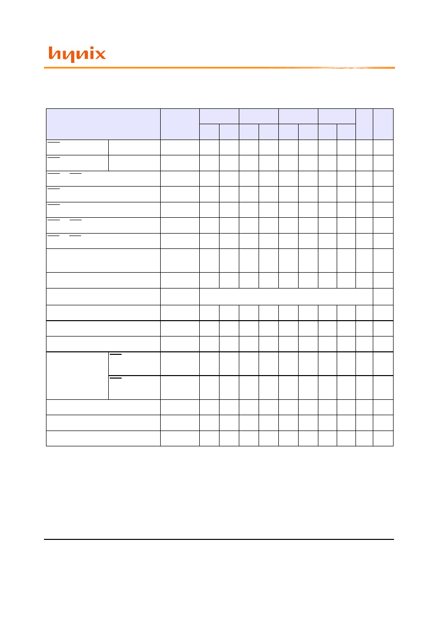
AC CHARACTERISTICS I
(AC operating conditions unless otherwise noted)
Note:
1. Assume t
R
/ t
F
(input rise and fall time) is 1ns. If t
R
& t
F
> 1ns, then [(t
R
+t
F
)/2-1]ns should be added to the parameter.
2. Access time to be measured with input signals of 1V/ns edge rate, from 0.8V to 0.2V. If t
R
> 1ns,
then (t
R
/2-0.5)ns should be added to the parameter.
Parameter
Sym-
bol
5
6
7
H
Unit Note
Min Max Min Max Min Max Min Max
System Clock
Cycle Time
CAS
Latency=3
t
CK3
5.0
1000
6.0
1000
7.0
1000
7.5
1000
ns
CAS
Latency=2
t
CK2
10
10
10
10
ns
Clock High Pulse Width
t
CHW
1.75
-
2.0
-
2.0
-
2.5
-
ns
1
Clock Low Pulse Width
t
CLW
1.75
-
2.0
-
2.0
-
2.5
-
ns
1
Access Time
From Clock
CAS
Latency=3
t
AC3
-
4.5
-
5.4
-
5.4
-
5.4
ns
2
CAS
Latency=2
t
AC2
-
6.0
-
6.0
-
6.0
-
6.0
ns
Data-out Hold Time
t
OH
2.0
-
2.0
-
2.5
-
2.5
-
ns
Data-Input Setup Time
t
DS
1.5
-
1.5
-
1.5
-
1.5
-
ns
1
Data-Input Hold Time
t
DH
0.8
-
0.8
-
0.8
-
0.8
-
ns
1
Address Setup Time
t
AS
1.5
-
1.5
-
1.5
-
1.5
-
ns
1
Address Hold Time
t
AH
0.8
-
0.8
-
0.8
-
0.8
-
ns
1
CKE Setup Time
t
CKS
1.5
-
1.5
-
1.5
-
1.5
-
ns
1
CKE Hold Time
t
CKH
0.8
-
0.8
-
0.8
-
0.8
-
ns
1
Command Setup Time
t
CS
1.5
-
1.5
-
1.5
-
1.5
-
ns
1
Command Hold Time
t
CH
0.8
-
0.8
-
0.8
-
0.8
-
ns
1
CLK to Data Output in Low-Z Time
t
OLZ
1.0
-
1.0
-
1.5
-
1.5
-
ns
CLK to
Data Output
in High-Z Time
CAS
Latency=3
t
OHZ3
-
4.5
-
5.4
-
5.4
-
5.4
ns
CAS
Latency=2
t
OHZ2
-
6.0
-
6.0
-
6.0
-
6.0
ns
Rev. 1.1 / Jan. 2005
11
Synchronous DRAM Memory 128Mbit (8Mx16bit)
HY57V281620E(L)T(P) Series
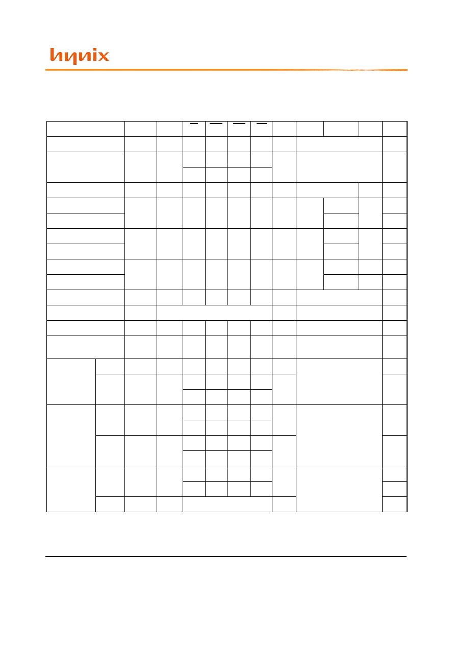
AC CHARACTERISTICS II
(AC operating conditions unless otherwise noted)
Note: 1. A new command can be given t
RRC
after self refresh exit.
Parameter
Symbol
5
6
7
H
Unit Note
Min Max Min Max Min Max Min Max
RAS Cycle Time
Operation
t
RC
55
-
60
-
63
-
63
-
ns
RAS Cycle Time
Auto Refresh
t
RRC
55
-
60
-
63
-
63
-
ns
RAS to CAS Delay
t
RCD
15
-
18
-
20
-
20
-
ns
RAS Active Time
t
RAS
38.7 100K
42 100K
42 100K
42 120K ns
RAS Precharge Time
t
RP
15
-
18
-
20
-
20
-
ns
RAS to RAS Bank Active Delay
t
RRD
10
-
12
-
14
-
15
-
ns
CAS to CAS Delay
t
CCD
1
-
1
-
1
-
1
-
CLK
Write Command to
Data-In Delay
t
WTL
0
-
0
-
0
-
0
-
CLK
Data-in to Precharge Command
t
DPL
2
-
2
-
2
-
2
-
CLK
Data-In to Active Command
t
DAL
t
DPL
+ t
RP
DQM to Data-Out Hi-Z
t
DQZ
2
-
2
-
2
-
2
-
CLK
DQM to Data-In Mask
t
DQM
0
-
0
-
0
-
0
-
CLK
MRS to New Command
t
MRD
2
-
2
-
2
-
2
-
CLK
Precharge to Data
Output High-Z
CAS
Latency=3
t
PROZ3
3
-
3
-
3
-
3
-
CLK
CAS
Latency=2
t
PROZ2
2
-
2
-
2
-
2
-
CLK
Power Down Exit Time
t
DPE
1
-
1
-
1
-
1
-
CLK
Self Refresh Exit Time
t
SRE
1
-
1
-
1
-
1
-
CLK
1
Refresh Time
t
REF
-
64
-
64
-
64
-
64
ms
Rev. 1.1 / Jan. 2005
12
Synchronous DRAM Memory 128Mbit (8Mx16bit)
HY57V281620E(L)T(P) Series
COMMAND TRUTH TABLE
Command
CKEn-1
CKEn
CS
RAS
CAS
WE
DQM
ADDR
A10/AP
BA
Note
Mode Register Set
H
X
L
L
L
L
X
OP code
No Operation
H
X
H
X
X
X
X
X
L
H
H
H
Bank Active
H
X
L
L
H
H
X
RA
V
Read
H
X
L
H
L
H
X
CA
L
V
Read with Autoprecharge
H
Write
H
X
L
H
L
L
X
CA
L
V
Write with Autoprecharge
H
Precharge All Banks
H
X
L
L
H
L
X
X
H
X
Precharge selected Bank
L
V
Burst Stop
H
X
L
H
H
L
X
X
DQM
H
X
V
X
Auto Refresh
H
H
L
L
L
H
X
X
Burst-Read-Single-WRITE
H
X
L
L
L
L
X
A9 ball High
(Other balls OP code)
MRS
Mode
Self Refresh
1
Entry
H
L
L
L
L
H
X
X
Exit
L
H
H
X
X
X
X
L
H
H
H
Precharge
power down
Entry
H
L
H
X
X
X
X
X
L
H
H
H
Exit
L
H
H
X
X
X
X
L
H
H
H
Clock
Suspend
Entry
H
L
H
X
X
X
X
X
L
V
V
V
Exit
L
H
X
X
Rev. 1.1 / Jan. 2005
13
Synchronous DRAM Memory 128Mbit (8Mx16bit)
HY57V281620E(L)T(P) Series
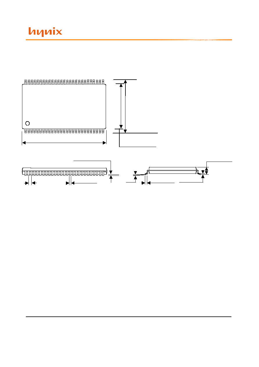
PACKAGE INFORMATION
400mil 54pin Thin Small Outline Package
11.938(0.4700)
11.735(0.4620)
10.262(0.4040)
10.058(0.3960)
22.327(0.8790)
22.149(0.8720)
5deg
0deg
0.597(0.0235)
0.406(0.0160)
0.210(0.0083)
0.120(0.0047)
1.194(0.0470)
0.991(0.0390)
0.80(0.0315)BSC
0.400(0.016)
0.300(0.012)
UNIT : mm(inch)
0.150(0.0059)
0.050(0.0020)