Document Outline
- Revision Details
- Contents
- 1. Description
- 1.1 Device Features & Ordering Information
- 1.2 Pin Configuration
- 1.2.1 128Mx4 DDR2 Pin Configuration
- 1.2.2 64Mx8 DDR2 PIN CONFIGURATION
- 1.2.3 32Mx16 DDR2 PIN CONFIGURATION
- 1.3 PIN DESCRIPTION
- 2. Functional Description
- 2.1 Simplified State Diagram
- 2.2 Functional Block Diagram
- 2.2.1 Functional Block Diagram(128Mx4)
- 2.2.2 Functioal Block Diagram (64Mx8)
- 2.2.3 Functional Block Diagram (32Mx16)
- 2.3 Basic Function & Operation of DDR2 SDRAM
- 2.3.1 Power up and Initialization
- 2.3.2 Programming the Mode and Extended Mode Registers
- 2.3.2.1 DDR2 SDRAM Mode Register Set (MRS)
- 2.3.2.2 DDR2 SDRAM Extended Mode Register Set
- 2.3.2.3 Off-Chip Driver (OCD) Impedance Adjustment
- 2.3.2.4 ODT (On Die Termination)
- 2.4 Bank Activate Command
- 2.5 Read and Write Access Modes
- 2.5.1 Posted CAS
- 2.5.2 Burst Mode Operation
- 2.5.3 Burst Read Command
- 2.5.4 Burst Write Operation
- 2.5.5 Write data mask
- 2.6 Precharge Operation
- 2.7 Auto Precharge Operation
- 2.8 Refresh Commands
- 2.8.1 Auto Refresh Command
- 2.8.2 Self Refresh Operation
- 2.9 Power-Down
- 2.10 Asynchronous CKE Low Event
- 2.11 No Operation Command
- 2.12 Deselect Command
- 3. Truth Tables
- 3.1 Command truth table.
- 3.2 Clock Enable (CKE) Truth Table for Synchronous Transitions
- 4. Operating Conditions
- 4.1 Absolute Maximum DC Ratings
- 4.2 Operating Temperature Condition
- 5. AC & DC Operating Conditons
- 5.1 DC Operation Conditions
- 5.1.1 Recommended DC Operating Conditions (SSTL_1.8)
- 5.1.2 ODT DC electrical characteristics
- 5.2 DC & AC Logic Input Levels
- 5.2.1 Input DC Logic Level
- 5.2.2 Input AC Logic Level
- 5.2.3 AC Input Test Conditions
- 5.2.4 Differential Input AC logic Level
- 5.2.5 Differential AC output parameters
- 5.2.6 Overshoot/Undershoot Specification
- 5.3 Output Buffer Levels
- 5.3.1 Output AC Test Conditions
- 5.3.2 Output DC Current Drive
- 5.3.3 OCD defalut characteristics
- 5.4 Default Output V-I characteristics
- 5.4.1 Full Strength Default Pulldown Driver Characteristics
- 5.4.2 Full Strength Default Pullup Driver Characteristics
- 5.4.3 Calibrated Output Driver V-I Characteristics
- 5.5 Input/Output Capacitance
- 6. IDD Specifications & Measurement Conditions
- 6.1 IDD Specifications
- 6.2 IDD Meauarement Conditions
- 7. AC Timing Specifications
- 7.1 Timing Parameters by Speed Grade
- 7.2 General notes, which may apply for all AC parameters
- 7.3 Specific Notes for dedicated AC parameters
- 8. Package Dimensions
- 8.1 Package Dimension(x4,x8)
- 8.2 Package Dimension(x16)

This document is a general product description and is subject to change without notice. Hynix Electronics does not assume
any responsibility for use of circuits described. No patent licenses are implied.
Rev 0.2 / Jan. 2004
1
HY5PS12421(L)F
HY5PS12821(L)F
HY5PS121621(L)F
512Mb DDR2 SDRAM
HY5PS12421(L)F
HY5PS12821(L)F
HY5PS121621(L)F
Rev 0.2 /Jan. 2004
2
HY5PS12421(L)F
HY5PS12821(L)F
HY5PS121621(L)F
Revision Details
Contents
1. Description
1.1 Device Features and Ordering Information
1.1.1 Key Feaures
1.1.2 Ordering Information
1.1.3 Ordering Frequency
1.2 Pin configuration
1.2.1 128M � 4 DDR2 Pin Configuration
1.2.2 64M � 8 DDR2 Pin Configuration
1.2.3 32M � 16 DDR2 Pin Configuration
1.3 Pin Description
2. Functioanal Description
2.1 Simplified State Diagram
2.2 Functional Block Diagram
2.2.1 Functional Block Diagram(128M � 4)
2.2.2 Functional Block Diagram(64M � 8)
2.2.3 Functional Block Diagram(32M � 16)
2.3 Basic Function & Operation of DDR2 SDRAM
2.3.1 Power up and Initialization
2.3.2 Programming the Mode and Extended Mode Registers
2.3.2.1 DDR2 SDRAM Mode Register Set(MRS)
2.3.2.2 DDR2 SDRAM Extended Mode Register Set
2.3.2.3 Off-Chip Driver(OCD) Impedance Adjustment
2.3.2.4 ODT(On Die Termination)
2.4 Bank Activate Command
2.5 Read and Write Command
2.5.1 Posted CAS
2.5.2 Burst Mode Operation
2.5.3 Burst Read Command
2.5.4 Burst Write Operation
2.5.5 Write Data Mask
2.6 Precharge Operation
2.7 Auto Precharge Operation
2.8 Refresh Commands
2.8.1 Auto Refresh Command
Revision No.
History
Draft Date Remark
0.0
1) Defined Target Spec.
Apr.2003
Preliminary
0.1
2) Change Some Description & IDD Spec
June 2003
0.2
1) Editorial clean up, Fixed CL3~6 & AL0~5,
2) Removed Vdd/Vddq=2.5V, Defined IDD Specifications,
3) Added Package outline, added Self-Refresh High temper-
ature Entry, changed tRAS spec. for DDR2 400
Dec. 2003

3
Rev 0.2 / Dec. 2003
HY5PS12421(L)F
HY5PS12821(L)F
HY5PS121621(L)F
2.8.2 Self Refresh Command
2.9 Power Down
2.10 Asynchronous CKE Low Event
2.11 No Operation Command
2.12 Deselect Command
3. Truth Tables
3.1 Command Truth Table
3.2 Clock Enable(CKE) Truth Table for Synchronous Transistors
3.3 Data Mask Truth Table
4. Operating Conditions
4.1 Absolute Maximum DC Ratings
4.2 Operating Temperature Condition
5. AC & DC Operating Conditions
5.1 DC Operation Conditions
5.1.1 Recommended DC Operating Conditions(SSTL_1.8)
5.1.2 ODT DC Electrical Characteristics
5.2 DC & AC Logic Input Levels
5.2.1 Input DC Logic Level
5.2.2 Input AC Logic Level
5.2.3 AC Input Test Conditions
5.2.4 Differential Input AC Logic Level
5.2.5 Differential AC output parameters
5.2.6 Overshoot / Undershoot Specification
5.3 Output Buffer Levels
5.3.1 Output AC Test Conditions
5.3.2 Output DC Current Drive
5.3.3 OCD default chracteristics
5.4 Default Output V-I Characteristics
5.4.1 Full Strength Default Pulldown Driver Characteristics
5.4.2 Full Strength Default Pullup Driver Chracteristics
5.4.3 Calibrated Output Driver V-I Characteristics
5.5 Input/Output Capacitance
6. IDD Specifications & Measurement Conditions
7. AC Timing Specifications
7.1 Timing Parameters by Speed Grade
7.2 General Notes for all AC Parameters
7.3 Specific Notes for dedicated AC parameters.
8 Package Dimensions
8.1 Package Dimension (x4 , x8)
8.2 Package Dimension(x16)
Rev 0.2 /Jan. 2004
4
HY5PS12421(L)F
HY5PS12821(L)F
HY5PS121621(L)F
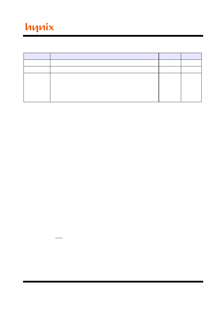
1.1 Device Features & Ordering Information
1.1.1 Key Features
� VDD=1.8V
� VDDQ=1.8V +/- 0.1V
� All inputs and outputs are compatible with SSTL_18 interface
� Fully differential clock inputs (CK, /CK) operation
� Double data rate interface
� Source synchronous-data transaction aligned to bidirectional data strobe (DQS, DQS)
� Differential Data Strobe (DQS, DQS)
� Data outputs on DQS, DQS edges when read (edged DQ)
� Data inputs on DQS centers when write(centered DQ)
� On chip DLL align DQ, DQS and DQS transition with CK transition
� DM mask write data-in at the both rising and falling edges of the data strobe
� All addresses and control inputs except data, data strobes and data masks latched on the rising
edges of the clock
� Programmable CAS latency 3, 4, 5 and 6 supported
� Programmable additive latency 0, 1, 2, 3, 4 and 5 supported
� Programmable burst length 4/8 with both nibble sequential and interleave mode
� Internal four bank operations with single pulsed RAS
� Auto refresh and self refresh supported
� tRAS lockout supported
� 8K refresh cycles /64ms
� JEDEC standard 60ball FBGA(x4/x8) & 84ball FBGA(x16)
� Full strength driver option controlled by EMRS
� On Die Termination supported
� Off Chip Driver Impedance Adjustment supported
� Read Data Strobe suupported (x8 only)
� Self-Refresh High Temperature Entry
Ordering Information
Part No.
Configuration Package
HY5PS12421(L)F-X*
128Mx4
60Ball
HY5PS12821(L)F-X*
64Mx8
HY5PS121621(L)F-X*
32Mx16
84Ball
Operating Frequency
Grade
tCK(ns)
CL
tRCD
tRP
Unit
-E3
5
3
3
3
Clk
-E4
5
4
4
4
Clk
-C4
3.75
4
4
4
Clk
-C5
3.75
5
5
5
Clk
-Y5
3
5
5
5
Clk
-Y6
3
6
6
6
Clk
Note: -X* is the speed bin, refer to the Operation
Frequency table for complete Part No.
1. Description

5
Rev 0.2 / Dec. 2003
HY5PS12421(L)F
HY5PS12821(L)F
HY5PS121621(L)F
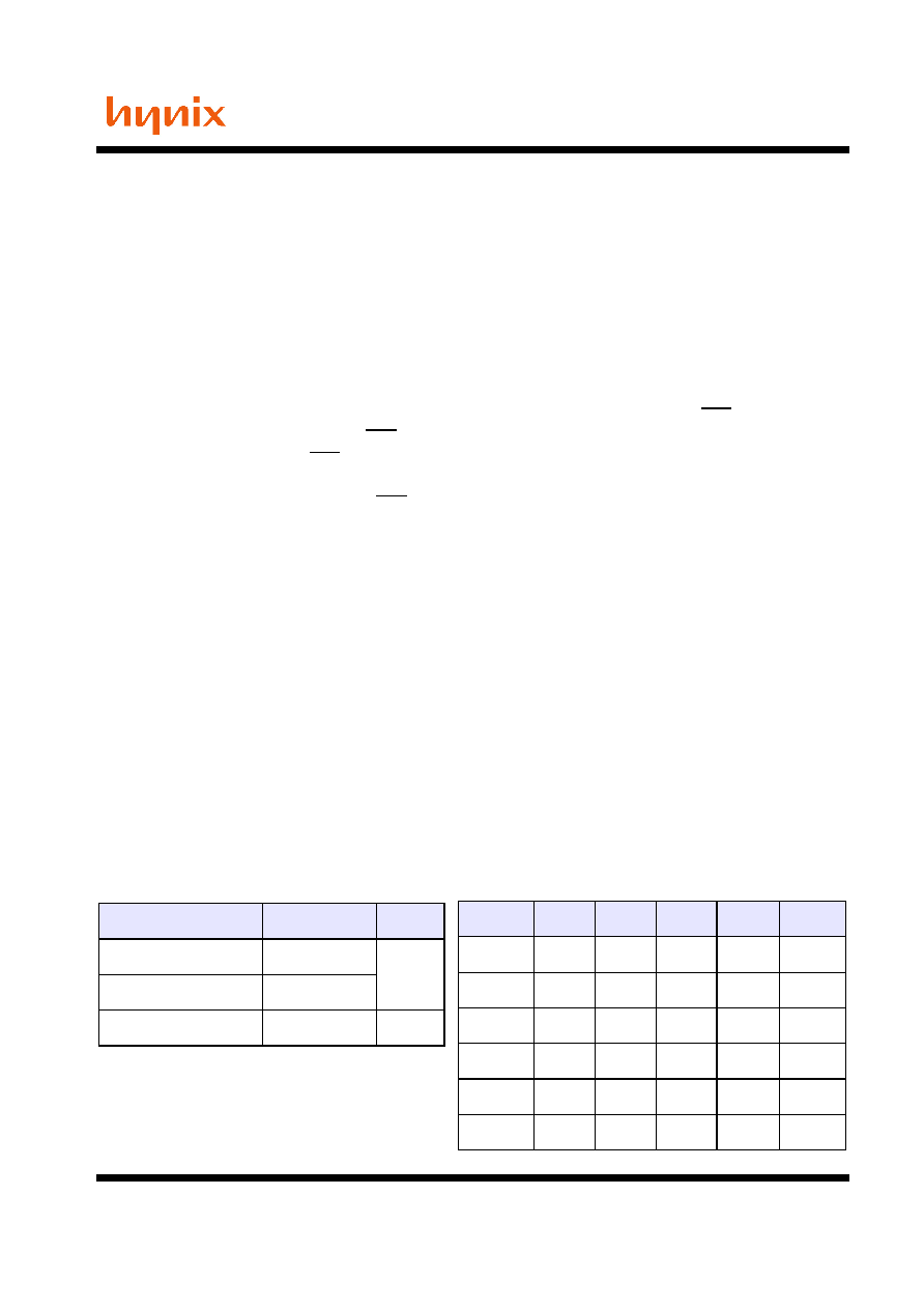
1.2 Pin Configuration
1.2.1 128Mx4 DDR2 Pin Configuration
3
VSS
DM
VDDQ
DQ3
VSS
WE
BA1
A1
A5
A9
NC
2
NC
VSSQ
DQ1
VSSQ
VREF
CKE
BA0
A10
A3
A7
A12
1
VDD
NC
VDDQ
NC
VDDL
NC
VSS
VDD
A
B
C
D
E
F
G
H
J
K
L
7
VSSQ
DQS
VDDQ
DQ2
VSSDL
RAS
CAS
A2
A6
A11
NC
8
DQS
VSSQ
DQ0
VSSQ
CK
CK
CS
A0
A4
A8
A13
9
VDDQ
NC
VDDQ
NC
VDD
ODT
VDD
VSS
ROW AND COLUMN ADDRESS TABLE
ITEMS
128Mx4
# of Bank
4
Bank Address
BA0, BA1
Auto Precharge Flag
A10/AP
Row Address
A0 - A13
Column Address
A0-A9, A11
Page size
1 KB