Document Outline
- Revision Details
- Contents
- 1. Description
- 1.1 Device Features & Ordering Information
- 1.1.1 Key Features
- 1.1.2 Ordering Information
- 1.1.3 Operating Frequency
- 1.2 Pin Configuration
- 1.2.1 64Mx4 DDR2 Pin Configuration
- 1.2.2 32Mx8 DDR2 PIN CONFIGURATION
- 1.2.3 16Mx16 DDR2 PIN CONFIGURATION
- 1.3 PIN DESCRIPTION
- 2. Functional Description
- 2.1 Simplified State Diagram
- 2.2 Functional Block Diagram
- 2.2.1 Functional Block Diagram(64Mx4)
- 2.2.2 Functioal Block Diagram (32Mx8)
- 2.2.3 Functional Block Diagram (16Mx16)
- 2.3 Basic Function & Operation of DDR2 SDRAM
- 2.3.1 Power up and Initialization
- 2.3.2 Programming the Mode and Extended Mode Registers
- 2.3.2.1 DDR2 SDRAM Mode Register Set (MRS)
- 2.3.2.2 DDR2 SDRAM Extended Mode Register Set
- 2.3.2.3 Off-Chip Driver (OCD) Impedance Adjustment
- 2.3.2.4 ODT (On Die Termination)
- 2.4 Bank Activate Command
- 2.5 Read and Write Command
- 2.5.1 Posted CAS
- 2.5.2 Burst Mode Operation
- 2.5.3 Burst Read Command
- 2.5.4 Burst Write Operation
- 2.5.5 Write Data Mask
- 2.6 Precharge Operation
- 2.7 Auto Precharge Operation
- 2.8 Refresh Commands
- 2.8.1 Auto Refresh Command
- 2.8.2 Self Refresh Operation
- 2.9 Power-Down
- 2. 10 Asynchronous CKE Low Event
- 2.11 No Operation Command
- 2.12 Deselect Command
- 3. Truth Tables
- 3.1 Command truth table.
- 3.2 Clock Enable (CKE) Truth Table for Synchronous Transitions
- 3.3 Data Mask Truth Table
- 4. Operating Conditions
- 4.1 Absolute Maximum DC Ratings
- 4.2 Operating Temperature Condition
- 5. AC & DC Operating Conditons
- 5.1 DC Operation Conditions
- 5.1.1 Recommended DC Operating Conditions (SSTL_1.8)
- 5.1.2 ODT DC electrical characteristics
- 5.2 DC & AC Logic Input Levels
- 5.2.1 Input DC Logic Level
- 5.2.2 Input AC Logic Level
- 5.2.3 AC Input Test Conditions
- 5.2.4 Differential Input AC logic Level
- 5.2.5 Differential AC output parameters
- 5.2.6 Overshoot/Undershoot Specification
- 5.3 Output Buffer Levels
- 5.3.1 Output AC Test Conditions
- 5.3.2 Output DC Current Drive
- 5.3.3 OCD defalut characteristics
- 5.4 Default Output V-I characteristics
- 5.4.1 Full Strength Default Pulldown Driver Characteristics
- 5.4.2 Full Strength Default Pullup Driver Characteristics
- 5.4.3 Calibrated Output Driver V-I Characteristics
- 5.5 Input/Output Capacitance
- 6. IDD Specifications & Measurement Conditions
- 6.1 IDD Specifications(tbd)
- 6.2 IDD Meauarement Conditions
- 7. AC Timing Specifications
- 7.1 Speed bins and tRCD,tRP and tRC for corresponding bin
- 7.2 Timing Parameters by Speed Grade
- 7.3 General notes, which may apply for all AC parameters
- 7.4 Specific Notes for dedicated AC parameters
- 8. Package Dimensions
- 8.1 Package Dimension(x4,x8)
- 8.2 Package Dimension(x16)

This document is a general product description and is subject to change without notice. Hynix Electronics does not assume
any responsibility for use of circuits described. No patent licenses are implied.
Rev 0.3 / May 2004
1
HY5PS56421(L)F
HY5PS56821(L)F
HY5PS561621(L)F
256Mb DDR2 SDRAM
HY5PS56421(L)F
HY5PS56821(L)F
HY5PS561621(L)F

Rev 0.3 / May 2004
2
HY5PS56421(L)F
HY5PS56821(L)F
HY5PS561621(L)F
Revision Details
Revision No.
History
Draft Date
Remark
0.1
Initial Release
Dec. 2003
Preliminary
0.2
Editorial clean up, changed tRAS spec. for DDR2 400
Jan. 2004
0.3
1) Defined IDD Spec.
2) Added Speed bins table in AC timming specification
May 2004

3
Rev 0.3 / May 2004
HY5PS12421(L)F
HY5PS12821(L)F
HY5PS121621(L)F
Contents
1. Description
1.1 Device Features and Ordering Information
1.1.1 Key Feaures
1.1.2 Ordering Information
1.1.3 Ordering Frequency
1.2 Pin configuration
1.2.1 64M � 4 DDR2 Pin Configuration
1.2.2 32M � 8 DDR2 Pin Configuration
1.2.3 16M � 16 DDR2 Pin Configuration
1.3 Pin Description
2. Functioanal Description
2.1 Simplified State Diagram
2.2 Functional Block Diagram
2.2.1 Functional Block Diagram(64M � 4)
2.2.2 Functional Block Diagram(32M � 8)
2.2.3 Functional Block Diagram(16M � 16)
2.3 Basic Function & Operation of DDR2 SDRAM
2.3.1 Power up and Initialization
2.3.2 Programming the Mode and Extended Mode Registers
2.3.2.1 DDR2 SDRAM Mode Register Set(MRS)
2.3.2.2 DDR2 SDRAM Extended Mode Register Set
2.3.2.3 Off-Chip Driver(OCD) Impedance Adjustment
2.3.2.4 ODT(On Die Termination)
2.4 Bank Activate Command
2.5 Read and Write Command
2.5.1 Posted CAS
2.5.2 Burst Mode Operation
2.5.3 Burst Read Command
2.5.4 Burst Write Operation
2.5.5 Write Data Mask
2.6 Precharge Operation
2.7 Auto Precharge Operation
2.8 Refresh Commands
2.8.1 Auto Refresh Command
2.8.2 Self Refresh Command
2.9 Power Down
2.10 Asynchronous CKE Low Event
2.11 No Operation Command
2.12 Deselect Command

Rev 0.3 / May 2004
4
HY5PS56421(L)F
HY5PS56821(L)F
HY5PS561621(L)F
3. Truth Tables
3.1 Command Truth Table
3.2 Clock Enable(CKE) Truth Table for Synchronous Transistors
3.3 Data Mask Truth Table
4. Operating Conditions
4.1 Absolute Maximum DC Ratings
4.2 Operating Temperature Condition
5. AC & DC Operating Conditions
5.1 DC Operation Conditions
5.1.1 Recommended DC Operating Conditions(SSTL_1.8)
5.1.2 ODT DC Electrical Characteristics
5.2 DC & AC Logic Input Levels
5.2.1 Input DC Logic Level
5.2.2 Input AC Logic Level
5.2.3 AC Input Test Conditions
5.2.4 Differential Input AC Logic Level
5.2.5 Differential AC output parameters
5.2.6 Overshoot / Undershoot Specification
5.3 Output Buffer Levels
5.3.1 Output AC Test Conditions
5.3.2 Output DC Current Drive
5.3.3 OCD default chracteristics
5.4 Default Output V-I Characteristics
5.4.1 Full Strength Default Pulldown Driver Characteristics
5.4.2 Full Strength Default Pullup Driver Chracteristics
5.4.3 Calibrated Output Driver V-I Characteristics
5.5 Input/Output Capacitance
6. IDD Specifications & Measurement Conditions
7. AC Timing Specifications
7.1 Speed bins and tRCD,tRP and tRC for corresponding bin
7.2 Timing Parameters by Speed Grade
7.3 General Notes for all AC Parameters
7.4 Specific Notes for dedicated AC parameters.
8 Package Dimensions
8.1 Package Dimension (x4 , x8)
8.2 Package Dimension(x16)

Rev 0.3 / May 2004
5
HY5PS56421(L)F
HY5PS56821(L)F
HY5PS561621(L)F
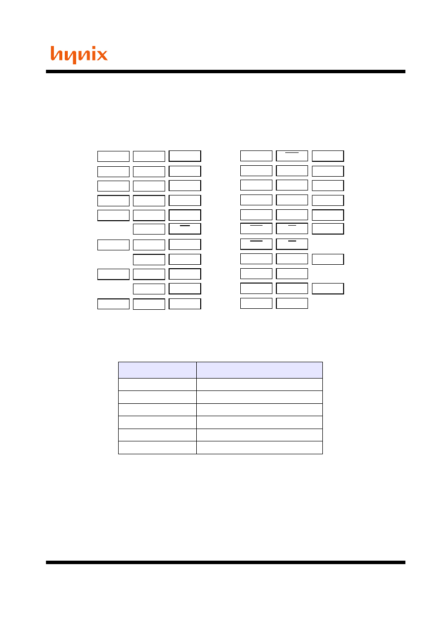
1.1 Device Features & Ordering Information
1.1.1 Key Features
� VDD=1.8V,2.2V
� VDDQ=1.8V +/- 0.1V
� All inputs and outputs are compatible with SSTL_18 interface
� Fully differential clock inputs (CK, /CK) operation
� Double data rate interface:tow data transfers per clock cycle(tCK)
� Source synchronous-data transaction aligned to bidirectional data strobe (DQS, DQS)
� Differential Data Strobe (DQS, DQS)
� Data outputs on DQS, DQS edges when read (edged DQ)
� Data inputs on DQS centers when write(centered DQ)
� On chip DLL align DQ, DQS and DQS transition with CK transition
� DM mask write data-in at the both rising and falling edges of the data strobe
� All addresses and control inputs except data, data strobes and data masks latched on the rising
edges of the clock
� Programmable CAS latency 2(optional), 3, 4, 5, 6 supported
� Programmable additive latency 0, 1, 2, 3, 4, 5 supported
� Programmable burst length 4/8 with both nibble sequential and interleave mode
� Internal four bank operations with single pulsed RAS
� Auto refresh and self refresh supported
� tRAS lockout supported
� 8K refresh cycles /64ms
� JEDEC standard 60ball FBGA(x4/x8) & 84ball FBGA(x16)
� Full strength driver option controlled by EMRS
� On Die Termination supported
� Off Chip Driver Impedance Adjustment supported
� Read Data Strobe suupported (x8 only)
Note:
-X* is the speed bin, refer to the Operation
Frequency table for complete Part No.
1. Description
1.1.3 Operating Frequency
Grade
tCK(ns)
CL
tRCD
tRP
Unit
-E3
5
3
3
3
Clk
-E4
5
4
4
4
Clk
-C4
3.75
4
4
4
Clk
-C5
3.75
5
5
5
Clk
-Y5
3
5
5
5
Clk
-Y6
3
6
6
6
Clk
1.1.2 Ordering Information
Part No.
Configuration Package
HY5PS56421(L)F-X*
64Mx4
60Ball
FBGA
HY5PS56821(L)F-X*
32Mx8
HY5PS561621(L)F-X*
16Mx16
84Ball
FBGA
Rev 0.3 / May 2004
6
HY5PS56421(L)F
HY5PS56821(L)F
HY5PS561621(L)F
1.2 Pin Configuration
1.2.1 64Mx4 DDR2 Pin Configuration
3
VSS
DM
VDDQ
DQ3
VSS
WE
BA1
A1
A5
A9
NC
2
NC
VSSQ
DQ1
VSSQ
VREF
CKE
BA0
A10
A3
A7
A12
1
VDD
NC
VDDQ
NC
VDDL
NC
VSS
VDD
A
B
C
D
E
F
G
H
J
K
L
7
VSSQ
DQS
VDDQ
DQ2
VSSDL
RAS
CAS
A2
A6
A11
NC
8
DQS
VSSQ
DQ0
VSSQ
CK
CK
CS
A0
A4
A8
NC
9
VDDQ
NC
VDDQ
NC
VDD
ODT
VDD
VSS
ROW AND COLUMN ADDRESS TABLE
ITEMS
64Mx4
# of Bank
4
Bank Address
BA0, BA1
Auto Precharge Flag
A10/AP
Row Address
A0 - A12
Column Address
A0-A9, A11
Page size
1 KB

Rev 0.3 / May 2004
7
HY5PS56421(L)F
HY5PS56821(L)F
HY5PS561621(L)F
1.2.2 32Mx8 DDR2 PIN CONFIGURATION
3
VSS
DM, RDQS
VDDQ
DQ3
VSS
WE
BA1
A1
A5
A9
NC
2
NU, RDQS
VSSQ
DQ1
VSSQ
VREF
CKE
BA0
A10
A3
A7
A12
1
VDD
DQ6
VDDQ
DQ4
VDDL
NC
VSS
VDD
A
B
C
D
E
F
G
H
J
K
L
7
VSSQ
DQS
VDDQ
DQ2
VSSDL
RAS
CAS
A2
A6
A11
NC
8
DQS
VSSQ
DQ0
VSSQ
CK
CK
CS
A0
A4
A8
NC
9
VDDQ
DQ7
VDDQ
DQ5
VDD
ODT
VDD
VSS
ROW AND COLUMN ADDRESS TABLE
ITEMS
32Mx8
# of Bank
4
Bank Address
BA0, BA1
Auto Precharge Flag
A10/AP
Row Address
A0 - A12
Column Address
A0-A9
Page size
1 KB

8
Rev 0.3 / May 2004
HY5PS12421(L)F
HY5PS12821(L)F
HY5PS121621(L)F
1.2.3 16Mx16 DDR2 PIN CONFIGURATION
3
VSS
UDM
VDDQ
DQ11
VSS
WE
BA1
A1
A5
A9
NC
2
NC
VSSQ
DQ9
VSSQ
VREF
CKE
BA0
A10
A3
A7
A12
1
VDD
DQ14
VDDQ
DQ12
VDDL
NC
VSS
VDD
A
B
C
D
J
K
L
M
N
P
R
7
VSSQ
UDQS
VDDQ
DQ10
VSSDL
RAS
CAS
A2
A6
A11
NC
8
UDQS
VSSQ
DQ8
VSSQ
CK
CK
CS
A0
A4
A8
NC
9
VDDQ
DQ15
VDDQ
DQ13
VDD
ODT
VDD
VSS
VSS
LDM
VDDQ
DQ3
NC
VSSQ
DQ1
VSSQ
VDD
DQ6
VDDQ
DQ4
E
F
G
H
VSSQ
LDQS
VDDQ
DQ2
LDQS
VSSQ
DQ0
VSSQ
VDDQ
DQ7
VDDQ
DQ5
ROW AND COLUMN ADDRESS TABLE
ITEMS
16Mx16
# of Bank
4
Bank Address
BA0, BA1
Auto Precharge Flag
A10/AP
Row Address
A0 - A12
Column Address
A0-A8
Page size
1 KB
Rev 0.3 / May 2004
9
HY5PS56421(L)F
HY5PS56821(L)F
HY5PS561621(L)F
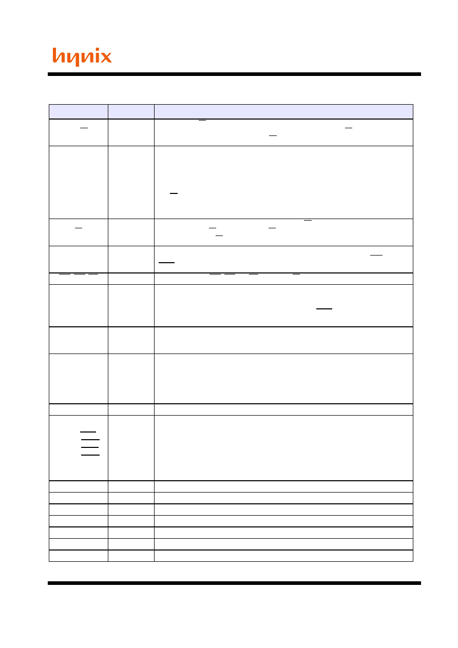
1.3 PIN DESCRIPTION
PIN
TYPE
DESCRIPTION
CK, CK
Input
Clock: CK and CK are differential clock inputs. All address and control input signals are sam-
pled on the crossing of the positive edge of CK and negative edge of CK. Output (read) data
is referenced to the crossings of CK and CK (both directions of crossing).
CKE
Input
Clock Enable: CKE HIGH activates, and CKE LOW deactivates internal clock signals, and
device input buffers and output drivers. Taking CKE LOW provides PRECHARGE POWER
DOWN and SELF REFRESH operation (all banks idle), or ACTIVE POWER DOWN (row
ACTIVE in any bank). CKE is synchronous for POWER DOWN entry and exit, and for SELF
REFRESH entry. CKE is asynchronous for SELF REFRESH exit, and for output disable. CKE
must be maintained high throughout READ and WRITE accesses. Input buffers, excluding
CK, CK and CKE are disabled during POWER DOWN. Input buffers, excluding CKE are dis-
abled during SELF REFRESH. CKE is an SSTL_18 input, but will detect an LVCMOS LOW level
after Vdd is applied.
CS
Input
Chip Select : Enables or disables all inputs except CK, CK, CKE, DQS and DM. All commands
are masked when CS is registered high. CS provides for external bank selection on systems
with multiple banks. CS is considered part of the command code.
ODT
Input
On Die Termination Control : ODT enables on die termination resistance internal to the
DDR2 SDRAM. When enabled, on die termination is only applied to DQ, DQS, DQS, RDQS,
RDQS, and DM.
RAS, CAS, WE
Input
Command Inputs: RAS, CAS and WE (along with CS) define the command being entered.
DM
(LDM, UDM)
Input
Input Data Mask : DM is an input mask signal for write data. Input Data is masked when DM
is sampled High coincident with that input data during a WRITE access. DM is sampled on
both edges of DQS, Although DM pins are input only, the DM loading matches the DQ and
DQS loading. For x8 device, the function of DM or RDQS/ RDQS is enabled by EMRS com-
mand.
BA0, BA1
Input
Bank Address Inputs: BA0 and BA1 define to which bank an ACTIVE, Read, Write or PRE-
CHARGE command is being applied. Bank address also determines if the mode register or
extended mode register is to be accessed during a MRS or EMRS cycle.
A0 ~ A12
Input
Address Inputs: Provide the row address for ACTIVE commands, and the column address
and AUTO PRECHARGE bit for READ/WRITE commands to select one location out of the
memory array in the respective bank. A10 is sampled during a precharge command to deter-
mine whether the PRECHARGE applies to one bank (A10 LOW) or all banks (A10 HIGH). If
only one bank is to be precharged, the bank is selected by BA0, BA1. The address inputs
also provide the op code during MODE REGISTER SET commands.
DQ
Input/Output
Data input / output : Bi-directional data bus
DQS, (DQS)
(UDQS),(UDQS)
(LDQS),(LDQS)
(RDQS),(RDQS)
Input/Output
Data Strobe : Output with read data, input with write data. Edge aligned with read data,
centered in write data. For the x16, LDQS correspond to the data on DQ0~DQ7; UDQS cor-
responds to the data on DQ8~DQ15. For the x8, an RDQS option using DM pin can be
enabled via the EMRS(1) to simplify read timing. The data strobes DQS, LDQS, UDQS, and
RDQS may be used in single ended mode or paired with optional complementary signals
DQS, LDQS,UDQS and RDQS to provide differential pair signaling to the system during both
reads and wirtes. An EMRS(1) control bit enables or disables all complementary data strobe
signals.
NC
No Connect : No internal electrical connection is present.
V
DDQ
Supply
DQ Ground
V
DDL
Supply
DLL Power Supply : 1.8V +/- 0.1V
V
SSDL
Supply
DLL Ground
VDD
Supply
Power Supply : 1.8V +/- 0.1V
V
SS
Supply
Ground
V
REF
Supply
Reference voltage for inputs for SSTL interface.

Rev 0.3 / May 2004
10
HY5PS56421(L)F
HY5PS56821(L)F
HY5PS561621(L)F
PIN
TYPE
DESCRIPTION
VDD
Supply
Power Supply : 1.8V +/- 0.1V
V
SS
Supply
Ground
V
REF
Supply
Reference voltage for inputs for SSTL interface.
In this data sheet, "differential DQS signals" refers to any of the following with A10 = 0 of EMRS(1)
x4 DQS/DQS
x8
DQS/DQS
if EMRS(1)[A11] = 0
x8 DQS/DQS, RDQS/RDQS,
if EMRS(1)[A11] = 1
x16 LDQS/LDQS and UDQS/UDQS
"single-ended DQS signals" refers to any of the following with A10 = 1 of EMRS(1)
x4
DQS
x8 DQS
if EMRS(1)[A11] = 0
x8 DQS, RDQS, if EMRS(1)[A11] = 1
x16 LDQS and UDQS
Rev 0.3 / May 2004
11
HY5PS56421(L)F
HY5PS56821(L)F
HY5PS561621(L)F
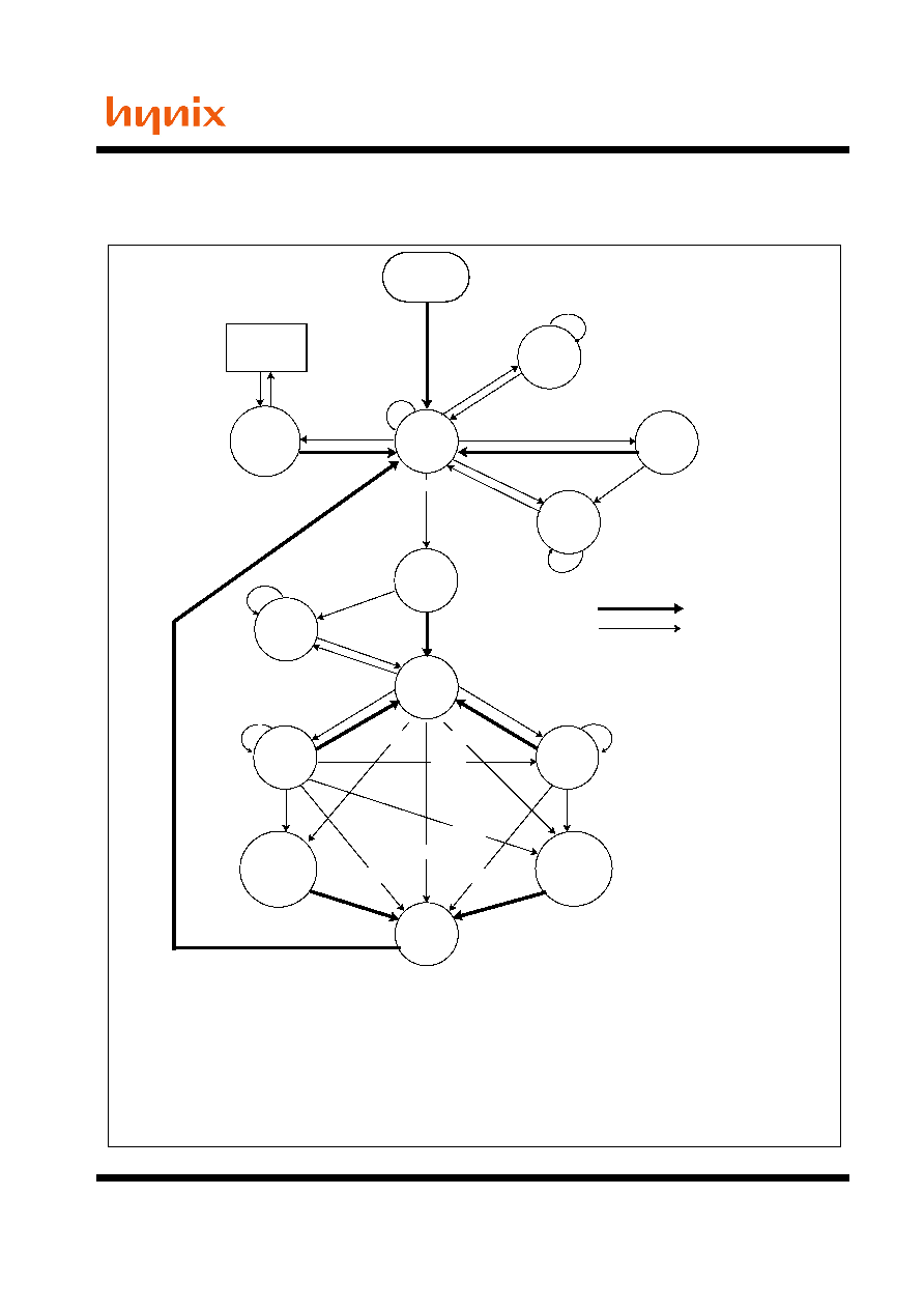
Self
Idle
Setting
EMRS
Bank
Precharging
Power
Writing
ACT
RDA
Read
SRF
REF
CKEL
MRS
CKEH
CKEH
CKEL
Write
Automatic Sequence
Command Sequence
RDA
WRA
Read
PR, PRA
PR
Refreshing
Refreshing
Down
Power
Down
Active
with
RDA
Reading
with
WRA
Active
Precharge
Reading
Writing
PR(A) = Precharge (All)
MRS = (Extended) Mode Register Set
SRF = Enter Self Refresh
REF = Refresh
CKEL = CKE low, enter Power Down
CKEH = CKE high, exit Power Down, exit Self Refresh
ACT = Activate
WR(A) = Write (with Autoprecharge)
RD(A) = Read (with Autoprecharge)
Note: Use caution with this diagram. It is indented to provide a floorplan of the possible state transitions
2.1 Simplified State Diagram
All banks
precharged
Activating
CKEH
Read
Write
CKEL
MRS
CKEL
Sequence
Initialization
OCD
calibration
CKEL
CKEL
CKEL
Autoprecharge
Autoprecharge
PR, PRA
PR, PRA
and the commands to control them, not all details. In particular situations involving more than one bank,
enabling/disabling on-die termination, Power Down enty/exit - among other things - are not captured
in full detail.
2. Functional Description
Rev 0.3 / May 2004
12
HY5PS56421(L)F
HY5PS56821(L)F
HY5PS561621(L)F
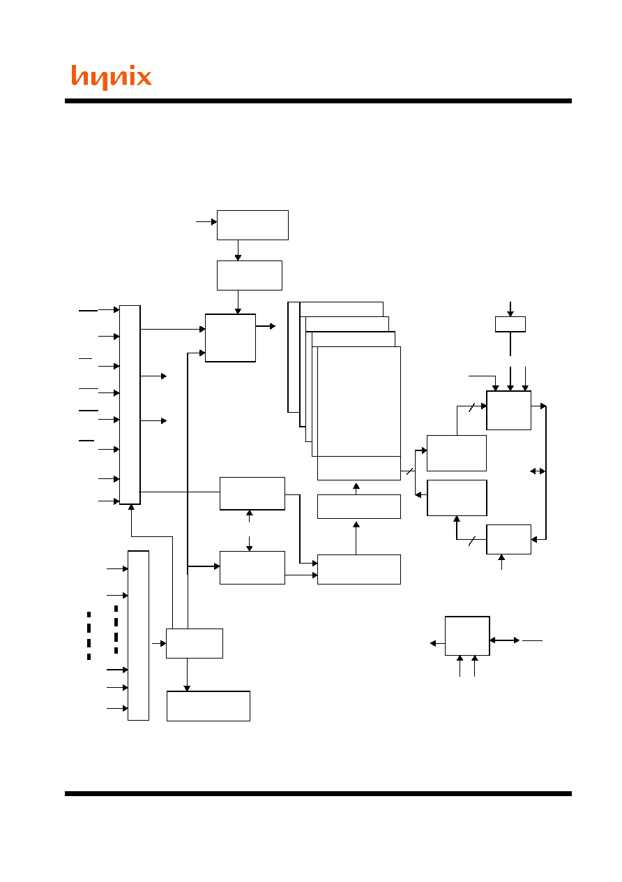
2.2 Functional Block Diagram
2.2.1 Functional Block Diagram(64Mx4)
4Banks x 16Mbit x 4 I/O DDR2 SDRAM
I
nput Buff
ers & State
Machin
e
Row
Pre
Decoders
Column
Pre Decoders
Self refresh
logic & timer
Internal Row
Counter
Row deco
der
s
16Mx4 Bank3
16Mx4 Bank2
16Mx4 Bank1
16Mx4 Bank0
Column decoders
Memory
Cell
Array
refresh
Column
Active
CLK
CLK
CKE
CS
RAS
CAS
WE
DM
Address
Registers
Column Add
Counter&latch
Mode
Register
Address bu
ffers
A0
A1
A12
BA1
BA0
Row
Active
bank select
Sense Amp
& I/O Gate
4bit pre-fetch
Read Data
Register
4bit pre-fetch
Write Data
Register
Column Active
latch
Additive Latency
Output
Buffers
& ODT
refresh
Input
Buffers
DLL Clk
OCD
Control
DQS
I/O Buffer
DQS
DQS
DLL
CLK
DS
DS
DQ
0~3
16
4
4
ODT
DLL Clk
OCD
Control
ODT
control
ODT
control

Rev 0.3 / May 2004
13
HY5PS56421(L)F
HY5PS56821(L)F
HY5PS561621(L)F
2.2.2 Functioal Block Diagram (32Mx8)
4Banks x 8Mbit x 8 I/O DDR2 SDRAM
Input
Buffers & St
ate Mach
ine
Row
Pre
Decoders
Column
Pre Decoders
Self refresh
logic & timer
Internal Row
Counter
Row decod
er
s
8Mx8 Bank3
8Mx8 Bank2
8Mx8 Bank1
8Mx8 Bank0
Column decoders
Memory
Cell
Array
refresh
Column
Active
CLK
CLK
CKE
CS
RAS
CAS
WE
DM
Address
Registers
Column Add
Counter&latch
Mode
Register
Addre
s
s buffers
A0
A1
A12
BA1
BA0
Row
Active
bank select
Sense Amp
& I/O Gate
4bit pre-fetch
Read Data
Register
4bit pre-fetch
Write Data
Register
Column Active
latch
Additive Latency
Output
Buffers
& ODT
refresh
Input
Buffers
DLL Clk
OCD
Control
DQS
I/O Buffer
&ODT
DQS
DQS
DLL
CLK
DS
DS
DQ
0~7
32
8
8
ODT
DLL Clk OCD
Control
ODT
control
ODT
control

Rev 0.3 / May 2004
14
HY5PS56421(L)F
HY5PS56821(L)F
HY5PS561621(L)F
2.2.3 Functional Block Diagram (16Mx16)
4Banks x 4Mbit x 16 I/O DDR2 SDRAM
In
put Buffe
rs & State
Machine
Row
Pre
Decoders
Column
Pre Decoders
Self refresh
logic & timer
Internal Row
Counter
Ro
w de
co
de
rs
4Mx16 Bank3
4Mx16 Bank2
4Mx16 Bank1
4Mx16 Bank0
Column decoders
Memory
Cell
Array
refresh
Column
Active
CLK
CLK
CKE
CS
RAS
CAS
WE
U/LDM
Address
Registers
Column Add
Counter&latch
Mode
Register
Addre
ss
buffers
A0
A1
A12
BA1
BA0
Row
Active
bank select
Sense Amp
& I/O Gate
4bit pre-fetch
Read Data
Register
4bit pre-fetch
Write Data
Register
Column Active
latch
Additive Latency
Output
Buffers
& ODT
refresh
Input
Buffers
DLL Clk
OCD
Control
DQS
I/O Buffer
&ODT
DQS
DQS
DLL
CLK
DS
DS
DQ
0~15
64
16
16
ODT
DLL Clk
OCD
Control
ODT
control
ODT
control
ODT
control

Rev 0.3 / May 2004
15
HY5PS56421(L)F
HY5PS56821(L)F
HY5PS561621(L)F
2.3 Basic Function & Operation of DDR2 SDRAM
Read and write accesses to the DDR2 SDRAM are burst oriented; accesses start at a selected location and
continue for a burst length of four or eight in a programmed sequence. Accesses begin with the registration of
an Active command, which is then followed by a Read or Write command. The address bits registered coinci-
dent with the active command are used to select the bank and row to be accessed (BA0-BA2 select the bank;
A0-A15 select the row). The address bits registered coincident with the Read or Write command are used to
select the starting column location for the burst access and to determine if the auto precharge command is to
be issued.
Prior to normal operation, the DDR2 SDRAM must be initialized. The following sections provide detailed infor-
mation covering device initialization, register definition, command descriptions and device operation.
2.3.1 Power up and Initialization
DDR2 SDRAMs must be powered up and initialized in a predefined manner. Operational procedures other
than those specified may result in undefined operation.
Power-up and Initialization Sequence
The following sequence is required for POWER UP and Initialization.
1. Apply power and attempt to maintain CKE below 0.2*VDDQ and ODT
*1
at a low state (all other inputs
may be undefined.)
- VDD, VDDL and VDDQ are driven from a single power converter output, AND
- VTT is limited to 0.95 V max, AND
- Vref tracks VDDQ/2.
or
- Apply VDD before or at the same time as VDDL.
- Apply VDDL before or at the same time as VDDQ.
- Apply VDDQ before or at the same time as VTT & Vref.
at least one of these two sets of conditions must be met.
2. Start clock and maintain stable condition.
3. For the minimum of 200
us after stable power and clock(CK, CK), then apply NOP or deselect & take
CKE high.
4. Wait minimum of 400ns then issue precharge all command. NOP or deselect applied during 400ns
period.
5. Issue EMRS(2) command. (To issue EMRS(2) command, provide "Low" to BA0 and BA2, "High" to
BA1.)
*2
6. Issue EMRS(3) command. (To issue EMRS(3) command, provide "Low" to BA2, "High" to BA0 and
BA1.)
*2
7. Issue EMRS to enable DLL. (To issue "DLL Enable" command, provide "Low" to A0, "High" to BA0 and
"Low" to BA1-2 and A13~A15.)
8. Issue a Mode Register Set command for "DLL reset".
(To issue DLL reset command, provide "High" to A8 and "Low" to BA0-2, and A13~15.)
9. Issue precharge all command.
10. Issue 2 or more auto-refresh commands.
11. Issue a mode register set command with low to A8 to initialize device operation. (i.e. to program operating
parameters without resetting the DLL.)
12. At least 200 clocks after step 8, execute OCD Calibration ( Off Chip Driver impedance adjustment ).

Rev 0.3 / May 2004
16
HY5PS56421(L)F
HY5PS56821(L)F
HY5PS561621(L)F
If OCD calibration is not used, EMRS OCD Default command (A9=A8= A7=1) followed by EMRS OCD
Calibration Mode Exit command (A9=A8=A7=0) must be issued with other operating parameters of
EMRS.
13. The DDR2 SDRAM is now ready for normal operation.
*1) To guarantee ODT off, VREF must be valid and a low level must be applied to the ODT pin.
*2) Sequence 5 and 6 may be performed between 8 and 9.
2.3.2 Programming the Mode and Extended Mode Registers
For application flexibility, burst length, burst type, CAS latency, DLL reset function, write recovery time(tWR)
are user defined variables and must be programmed with a Mode Register Set (MRS) command. Addition-
ally, DLL disable function, driver impedance, additive CAS latency, ODT(On Die Termination), single-ended
strobe, and OCD(off chip driver impedance adjustment) are also user defined variables and must be pro-
grammed with an Extended Mode Register Set (EMRS) command. Contents of the Mode Register(MR) or
Extended Mode Registers(EMR(#)) can be altered by re-executing the MRS and EMRS Commands. If the
user chooses to modify only a subset of the MRS or EMRS variables, all variables must be redefined when
the MRS or EMRS commands are issued.
MRS, EMRS and Reset DLL do not affect array contents, which means reinitialization including those can be
executed any time after power-up without affecting array contents.
Initialization Sequence after Power Up
/CK
CK
CKE
Command
PRE
ALL
PRE
ALL
EMRS
MRS
REF
REF
MRS
EMRS
EMRS
ANY
CMD
DLL
ENABLE
DLL
RESET
OCD
Default
OCD
CAL. MODE
EXIT
Follow OCD
Flowchart
400ns
tRFC
tRFC
tRP
tRP
tMRD
tMRD
tMRD
tOIT
min. 200 Cycle
NOP
ODT
tCL
tCH
tIS

Rev 0.3 / May 2004
17
HY5PS56421(L)F
HY5PS56821(L)F
HY5PS561621(L)F
2.3.2.1 DDR2 SDRAM Mode Register Set (MRS)
The mode register stores the data for controlling the various operating modes of DDR2 SDRAM. It controls
CAS latency, burst length, burst sequence, test mode, DLL reset, tWR and various vendor specific options to
make DDR2 SDRAM useful for various applications. The default value of the mode register is not defined,
therefore the mode register must be written after power-up for proper operation. The mode register is written
by asserting low on CS, RAS, CAS, WE, BA0 and BA1, while controlling the state of address pins A0 ~ A15.
The DDR2 SDRAM should be in all bank precharge with CKE already high prior to writing into the mode reg-
ister. The mode register set command cycle time (tMRD) is required to complete the write operation to the
mode register. The mode register contents can be changed using the same command and clock cycle
requirements during normal operation as long as all banks are in the precharge state. The mode register is
divided into various fields depending on functionality. Burst length is defined by A0 ~ A2 with options of 4 and
8 bit burst lengths. The burst length decodes are compatible with DDR SDRAM. Burst address sequence type
is defined by A3, CAS latency is defined by A4 ~ A6. The DDR2 doesn't support half clock latency mode. A7
is used for test mode. A8 is used for DLL reset. A7 must be set to low for normal MRS operation. Write recov-
ery time tWR is defined by A9 ~ A11. Refer to the table for specific codes.
Address Field
CAS Latency
A
6
A
5
A
4
Latency
0
0
0
Reserved
0
0
1
Reserved
0
1
0
2(optional)
0
1
1
3
1
0
0
4
1
0
1
5
1
1
0
6
1
1
1
Reserved
A
7
mode
0
Normal
1
Test
A
3
Burst Type
0
Sequential
1
Interleave
A
8
DLL Reset
0
No
1
Yes
Mode Register
BA
1
BA
0
A
11
A
10
A
9
A
8
A
7
A
6
A
5
A
4
A
3
A
2
A
1
A
0
0
TM
CAS Latency
BT
DLL
0*
1
WR
Write recovery for autoprecharge
A
11
A
10
A
9
WR(cycles)
0
0
0
Reserved
0
0
1
2
0
1
0
3
0
1
1
4
1
0
0
5
1
0
1
6
1
1
0
Reserved
1
1
1
Reserved
A
15
~ A
13
0
Burst Length
Burst Length
A
2
A
1
A
0
BL
0
1
0
4
0
1
1
8
*1 : BA2 and A13~A15 are reserved for future use and must be programmed to 0 when setting the mode register.
* 2: WR(write recovery for autoprecharge) min is determined by tCK max and WR max is determined by tCK min.
WR in clock cycles is calculated by dividing tWR (in ns) by tCK (in ns) and rounding up to the next integer
(WR[cycles] = tWR(ns)/tCK(ns)). The mode register must be programmed to this value. This is also used with
tRP to determine tDAL.
BA
2
0*
1
BA1
BA0
MRS mode
0
0
MRS
0
1
EMRS(1)
1
0
EMRS(2): Reserved
1
1
EMRS(3): Reserved
DD
R400
DDR
533
DD
R667
DDR8
00
*2
A
12
PD
A
12
Active power
down exit time
0
Fast exit(use t
XARD
)
1
Slow exit(use t
XARDS
)

Rev 0.3 / May 2004
18
HY5PS56421(L)F
HY5PS56821(L)F
HY5PS561621(L)F
2.3.2.2 DDR2 SDRAM Extended Mode Register Set
EMRS(1)
The extended mode register(1) stores the data for enabling or disabling the DLL, output driver strength, additive latency,
ODT, DQS disable, OCD program, RDQS enable. The default value of the extended mode register(1) is not defined,
therefore the extended mode register(1) must be written after power-up for proper operation. The extended mode regis-
ter(1) is written by asserting low on CS, RAS, CAS, WE, high on BA0 and low on BA1, while controlling the states of
address pins A0 ~ A15. The DDR2 SDRAM should be in all bank precharge with CKE already high prior to writing into the
extended mode register(1). The mode register set command cycle time (tMRD) must be satisfied to complete the write
operation to the extended mode register(1). Mode register contents can be changed using the same command and clock
cycle requirements during normal operation as long as all banks are in the precharge state. A0 is used for DLL enable or
disable. A1 is used for enabling a half strength output driver. A3~A5 determines the additive latency, A7~A9 are used for
OCD control, A10 is used for DQS disable and A11 is used for RDQS enable. A2 and A6 are used for ODT setting.
DLL Enable/Disable
The DLL must be enabled for normal operation. DLL enable is required during power up initialization, and
upon returning to normal operation after having the DLL disabled. The DLL is automatically disabled when
entering self refresh operation and is automatically re-enabled upon exit of self refresh operation. Any time
the DLL is enabled (and subsequently reset), 200 clock cycles must occur before a Read command can be
issued to allow time for the internal clock to be synchronized with the external clock. Failing to wait for syn-
chronization to occur may result in a violation of the tAC or tDQSCK parameters.

Rev 0.3 / May 2004
19
HY5PS56421(L)F
HY5PS56821(L)F
HY5PS561621(L)F
Address Field
RDQS
Extended Mode Register
DLL
0*
1
D.I.C
BA
0
A
15 ~
A
13
A
11
A
10
A
9
A
8
A
7
A
6
A
5
A
4
A
3
A
2
A
1
A
0
A
0
DLL Enable
0
Enable
1
Disable
Additive latency
A
5
A
4
A
3
Additive Latency
0
0
0
0
0
0
1
1
0
1
0
2
0
1
1
3
1
0
0
4
1
0
1
5
1
1
0
Reserved
1
1
1
Reserved
a: When Adjust mode is issued, AL from previously set value must be applied.
b: After setting to default, OCD mode needs to be exited by setting A9-A7 to
000. Refer to the following 2.2.2.3 section for detailed information
A9 A8
A7
OCD Calibration Program
0
0
0 OCD Calibration mode exit; maintain setting
0
0
1 Drive(1)
0
1
0 Drive(0)
1
0
0 Adjust mode
a
1
1
1 OCD Calibration default
b
OCD program
1
DQS
Rtt
Rtt
A1
Output Driver
Impedence Control
Driver
Size
0
Normal 100%
1
Half
60%
A10
DQS
0
Enable
1
Disable
* If RDQS is enabled, the
DM function is disabled. RDQS
is active for reads and don't
care for writes.
A11
RDQS Enable
0
Disable
1
Enable
*1 : BA2 and A13~A15 are reserved for future use and must be programmed to 0 when setting the mode register.
BA
1
0
A6
A2 R
tt
(
NOMINAL
)
0
0
ODT Disabled
0
1
75 ohm
1
0
150 ohm
1
1
Reserved
BA1
BA0
MRS mode
0
0
MRS
0
1
EMRS(1)
1
0
EMRS(2): Reserved
1
1
EMRS(3): Reserved
BA
2
0*
1
EMRS(1) Programming
Qoff
A
12
A
12
Qoff (Optional)
a
a.
Outputs disabled - DQs, DQSs, DQSs,
RDQS, RDQS. This feature is used in
conjunction with DIMM IDD meaurements when
IDDQ is not desired to
be included.
0
Output buffer enabled
1
Output buffer disabled
A11
(RDQS Enable)
A10
(DQS Disable)
Strobe Function Matrix
RDQS/DM
RDQS
DQS
DQS
0 (Disable)
0 (Enable)
DM
Hi-z
DQS
DQS
0 (Disable)
1 (Disable)
DM
Hi-z
DQS
Hi-z
1 (Enable)
0 (Enable)
RDQS
RDQS
DQS
DQS
1 (Enable)
1 (Disable)
RDQS
Hi-z
DQS
Hi-z

Rev 0.3 / May 2004
20
HY5PS56421(L)F
HY5PS56821(L)F
HY5PS561621(L)F
EMRS(2)
The extended mode register(2) controls refresh related features. The default value of the extended mode reg-
ister(2) is not defined, therefore the extended mode register(2) must be written after power-up for proper
operation. The extended mode register(2) is written by asserting low on /CS,/RAS,/CAS,/WE, high on BA1
and low on BA0, while controling the states of address pins A0~A15. The DDR2 SDRAM should be in all bank
precharge with CKE already high prior to writing into the extended mode register(2). Mode register contents
can be changed using the same command and clock cycle requirements during normal operation as long as
all bank are in the precharge state.
EMRS(2) Programming:
*1 : The rest bits in EMRS(2) is reserved for future use and all bits except A7, BA0 and BA1 must be
programmed to 0 when setting the mode register during initialization.
Due to the migration natural, user needs to ensure the DRAM part supports higher than 85 Tcase tempera-
ture self-refresh entry. JEDEC standard DDR2 SDRAM Module user can look at DDR2 SDRAM Module SPD
fileld Byte 49 bit[0]. If the high temperature self-refresh mode is supported then controller can set the EMRS2
[A7] bit to enable the self-refresh rate in case of higher than 85 temperature self-refresh operation. For the
lose part user, please refer to the Hynix web site(www.hynix.com) to check the high temperature self-refresh
rate availability.
EMRS(3) Programming: Reserved
*
1
*1 : EMRS(3) is reserved for future use and all bits except BA0 and BA1 must be programmed to 0 when setting
the mode register during initialization.
Address Field
Extended Mode
0*
1
BA
0
A
15 ~
A
13
A
11
A
10
A
9
A
8
A
7
A
6
A
5
A
4
A
3
A
2
A
1
A
0
0
BA
1
1
BA
2
0*
1
A
12
SRF
0*
1
Register(2)
0*
1
BA
0
A
15 ~
A
13
A
11
A
10
A
9
A
8
A
7
A
6
A
5
A
4
A
3
A
2
A
1
A
0
1
BA
1
1
BA
2
0*
1
A
12
BA1
BA0
MRS mode
0
0
MRS
0
1
EMRS(1)
1
0
EMRS(2)
1
1
EMRS(3):Reserved
A7
Hign Temp Self-refresh
Rate Enable
1
Enable
0
Disable

Rev 0.3 / May 2004
21
HY5PS56421(L)F
HY5PS56821(L)F
HY5PS561621(L)F
2.3.2.3 Off-Chip Driver (OCD) Impedance Adjustment
DDR2 SDRAM supports driver calibration feature and the flow chart below is an example of sequence. Every
calibration mode command should be followed by "OCD calibration mode exit" before any other command
being issued.
MRS should be set before entering OCD impedance adjustment and ODT (On Die Termian-
tion) should be carefully controlled depending on system environment.
Start
EMRS: Drive(1)
DQ & DQS High; DQS Low
Test
EMRS :
Enter Adjust Mode
BL=4 code input to all DQs
Inc, Dec, or NOP
EMRS: Drive(0)
DQ & DQS Low; DQS High
Test
EMRS :
Enter Adjust Mode
BL=4 code input to all DQs
Inc, Dec, or NOP
EMRS: OCD calibration mode exit
End
ALL OK
ALL OK
Need Calibration
Need Calibration
EMRS: OCD calibration mode exit
EMRS: OCD calibration mode exit
EMRS: OCD calibration mode exit
EMRS: OCD calibration mode exit
EMRS: OCD calibration mode exit
MRS shoud be set before entering OCD impedance adjustment and ODT should
be carefully controlled depending on system environment

Rev 0.3 / May 2004
22
HY5PS56421(L)F
HY5PS56821(L)F
HY5PS561621(L)F
Extended Mode Register Set for OCD impedance adjustment
OCD impedance adjustment can be done using the following EMRS mode. In drive mode all outputs are
driven out by DDR2 SDRAM and drive of RDQS is depedent on EMRS bit enabling RDQS operation. In
Drive(1) mode, all DQ, DQS (and RDQS) signals are driven high and all DQS signals are driven low. In
drive(0) mode, all DQ, DQS (and RDQS) signals are driven low and all DQS signals are driven high. In adjust
mode, BL = 4 of operation code data must be used. In case of OCD calibration default, output driver charac-
teristics have a nominal impedance value of 18 ohms during nominal temperature and voltage conditions.
Output driver characteristics for OCD calibration default are specified in Table x. OCD applies only to normal
full strength output drive setting defined by EMRS(1) and if half strength is set, OCD default output driver
characteristics are not applicable. When OCD calibration adjust mode is used, OCD default output driver
characteristics are not applicable. After OCD calibration is completed or driver strength is set to default,
subsequent EMRS commands not intended to adjust OCD characteristics must specify A9-A7 as '000' in
order to maintain the default or calibrated value.
Off- Chip-Driver program
OCD impedance adjust
To adjust output driver impedance, controllers must issue the ADJUST EMRS command along with a 4bit
burst code to DDR2 SDRAM as in table X. For this operation, Burst Length has to be set to BL = 4 via MRS
command before activating OCD and controllers must drive this burst code to all DQs at the same time. DT0
in table X means all DQ bits at bit time 0, DT1 at bit time 1, and so forth. The driver output impedance is
adjusted for all DDR2 SDRAM DQs simultaneously and after OCD calibration, all DQs of a given DDR2
SDRAM will be adjusted to the same driver strength setting. The maximum step count for adjustment is 16
and when the limit is reached, further increment or decrement code has no effect. The default setting may be
any step within the 16 step range. When Adjust mode command is issued, AL from previously set value must
be applied
Table X :
Off- Chip-Driver Program
A9
A8
A7
Operation
0
0
0
OCD calibration mode exit
0
0
1
Drive(1) DQ, DQS, (RDQS) high and DQS low
0
1
0
Drive(0) DQ, DQS, (RDQS) low and DQS high
1
0
0
Adjust mode
1
1
1
OCD calibration default
4bit burst code inputs to all DQs
Operation
D
T0
D
T1
D
T2
D
T3
Pull-up driver strength
Pull-down driver strength
0
0
0
0
NOP (No operation)
NOP (No operation)
0
0
0
1
Increase by 1 step
NOP
0
0
1
0
Decrease by 1 step
NOP
0
1
0
0
NOP
Increase by 1 step
1
0
0
0
NOP
Decrease by 1 step
0
1
0
1
Increase by 1 step
Increase by 1 step
0
1
1
0
Decrease by 1 step
Increase by 1 step
1
0
0
1
Increase by 1 step
Decrease by 1 step
1
0
1
0
Decrease by 1 step
Decrease by 1 step
Other Combinations
Reserved

Rev 0.3 / May 2004
23
HY5PS56421(L)F
HY5PS56821(L)F
HY5PS561621(L)F
For proper operation of adjust mode, WL = RL - 1 = AL + CL - 1 clocks and tDS/tDH should be met as the fol-
lowing timing diagram. For input data pattern for adjustment, DT0 - DT3 is a fixed order and "not affected by
MRS addressing mode (ie. sequential or interleave).
Drive Mode
Drive mode, both Drive(1) and Drive(0), is used for controllers to measure DDR2 SDRAM Driver impedance.
In this mode, all outputs are driven out tOIT after "enter drive mode" command and all output drivers are
turned-off tOIT after "OCD calibration mode exit" command as the following timing diagram.
NOP
NOP
NOP
NOP
EMRS
D
T0
CMD
CK
DQS_in
DQ_in
tDS tDH
WL
OCD adjust mode
OCD calibration mode exit
D
T1
D
T2
D
T3
WR
EMRS
NOP
NOP
CK
DQS
DM
EMRS
NOP
NOP
NOP
EMRS
CMD
CK
DQS
DQ
Enter Drive mode
OCD calibration mode exit
tOIT
Hi-Z
DQs high for Drive(1)
DQS high & DQS low for Drive(1), DQS low & DQS high for Drive(0)
Hi-Z
DQs low for Drive(0)
tOIT
CK
DQS

Rev 0.3 / May 2004
24
HY5PS56421(L)F
HY5PS56821(L)F
HY5PS561621(L)F
2.3.2.4 ODT (On Die Termination)
On Die Termination (ODT) is a feature that allows a DRAM to turn on/off termination resistance for each DQ,
DQS/DQS, RDQS/RDQS, and DM signal for x4x8 configurations via the ODT control pin. For x16 configura-
tion ODT is applied to each DQ, UDQS/UDQS, LDQS/LDQS, UDM, and LDM signal via the ODT control pin.
The ODT feature is designed to improve signal integrity of the memory channel by allowing the DRAM con-
troller to independently turn on/off termination resistance for any or all DRAM devices.
The ODT function is supported for ACTIVE and STANDBY modes. ODT is turned off and not supported in
SELF REFRESH mode.
FUNCTIONAL REPRESENTATION OF ODT
Input
Pin
Input
Buffer
DRAM
V
SS
Q
V
SS
Q
V
DD
Q
V
DD
Q
Rval2
Rval2
Rval1
Rval1
sw1
sw1
sw2
sw2
Selection between sw1 or sw2 is determined by "Rtt (nominal)" in EMRS
Termination included on all DQs, DM, DQS, DQS, RDQS, and RDQS pins.
Switch sw1 or sw2 is enabled by ODT pin.
Target Rtt (ohm) = (Rval1) / 2 or (Rval2) / 2

Rev 0.3 / May 2004
25
HY5PS56421(L)F
HY5PS56821(L)F
HY5PS561621(L)F
ODT timing for active/standby mode
ODT timing for powerdown mode
T0
T1
T2
T3
T4
T5
tAOND
CK
CK
CKE
ODT
Internal
Term Res.
T6
tAOFD
tIS
tIS
tAON,min
tAON,max
tAOF,min
tAOF,max
R
TT
T0
T1
T2
T3
T4
T5
CK
CK
CKE
ODT
Internal
Term Res.
T6
tIS
tIS
tAONPD,min
tAOFPD,max
tAONPD,max
tAOFPD,min
R
TT

Rev 0.3 / May 2004
26
HY5PS56421(L)F
HY5PS56821(L)F
HY5PS561621(L)F
ODT timing mode switch at entering power down mode
T-5
T-4
T-3
T-2
T-1
T0
CK
CK
T1
CKE
ODT
Internal
Term Res.
tIS
tAOFD
RTT
tIS
RTT
T2
T3
T4
ODT
Internal
Term Res.
Active & Standby
mode timings to
be applied.
Power Down
mode timings to
be applied.
tAOFPDmax
tIS
ODT
Internal
Term Res.
tIS
tAOND
RTT
tIS
RTT
ODT
Internal
Term Res.
Active & Standby
mode timings to
be applied.
Power Down
mode timings to
be applied.
tAONPDmax
tANPD
Entering Slow Exit Active Power Down Mode
or Precharge Power Down Mode.

Rev 0.3 / May 2004
27
HY5PS56421(L)F
HY5PS56821(L)F
HY5PS561621(L)F
ODT timing mode switch at exiting power down mode
T0
T1
T4
T5
T6
T7
CK
CK
T8
CKE
ODT
Internal
Term Res.
tIS
tAOFPDmax
RTT
tIS
tIS
RTT
T9
T10
T11
ODT
Internal
Term Res.
tAXPD
Active & Standby
mode timings to
be applied.
Power Down
mode timings to
be applied.
Exiting from Slow Active Power Down Mode
or Precharge Power Down Mode.
tAOFD
Internal
Term Res.
tIS
RTT
ODT
Active & Standby
mode timings to
be applied.
tAOND
Internal
Term Res.
RTT
ODT
tAONPDmax
tIS
Power Down
mode timings to
be applied.

Rev 0.3 / May 2004
28
HY5PS56421(L)F
HY5PS56821(L)F
HY5PS561621(L)F
2.4 Bank Activate Command
The Bank Activate command is issued by holding CAS and WE high with CS and RAS low at the rising edge
of the clock. The bank addresses BA0 ~ BA2 are used to select the desired bank. The row address A0
through A15 is used to determine which row to activate in the selected bank. The Bank Activate command
must be applied before any Read or Write operation can be executed. Immediately after the bank active
command, the DDR2 SDRAM can accept a read or write command on the following clock cycle. If a R/W
command is issued to a bank that has not satisfied the tRCDmin specification, then additive latency must be
programmed into the device to delay when the R/W command is internally issued to the device. The additive
latency value must be chosen to assure tRCDmin is satisfied. Additive latencies of 0, 1, 2, 3 and 4 are sup-
ported. Once a bank has been activated it must be precharged before another Bank Activate command can
be applied to the same bank. The bank active and precharge times are defined as tRAS and tRP, respec-
tively. The minimum time interval between successive Bank Activate commands to the same bank is deter-
mined by the RAS cycle time of the device (t
RC
). The minimum time interval between Bank Activate
commands is t
RRD
.
Bank Activate Command Cycle: tRCD = 3, AL = 2, tRP = 3, tRRD = 2, tCCD = 2
ADDRESS
CK / CK
T0
T2
T1
T3
Tn
Tn+1
Tn+2
Tn+3
COMMAND
Bank A
Row Addr.
Bank A
Activate
Bank A
Col. Addr.
. . . . . . . . . .
. . . . . . . . . .
. . . . . . . . . .
Internal RAS-CAS delay (>=
t
RCDmin
)
: "H" or "L"
RAS Cycle time (
>= t
RC
)
additive latency delay (
AL
)
Read
Bank B
Row Addr.
Bank B
Activate
Bank B
Col. Addr.
Bank A
Bank A
Precharge
Bank B
Addr.
Bank B
Precharge
Bank A
Row Addr.
Activate
Bank A
RAS - RAS delay time (
>= t
RRD
)
Read Begins
tRCD =1
Addr.
Bank Active
(>= t
RAS
)
Bank Precharge time (
>= t
RP
)
CAS-CAS delay time (
t
CCD
)
Bank A
Post CAS
Read
Bank B
Post CAS

Rev 0.3 / May 2004
29
HY5PS56421(L)F
HY5PS56821(L)F
HY5PS561621(L)F
2.5 Read and Write Command
After a bank has been activated, a read or write cycle can be executed. This is accomplished by setting RAS
high, CS and CAS low at the clock's rising edge. WE must also be defined at this time to determine whether
the access cycle is a read operation (WE high) or a write operation (WE low).
The DDR2 SDRAM provides a fast column access operation. A single Read or Write Command will initiate a
serial read or write operation on successive clock cycles. The boundary of the burst cycle is strictly restricted
to specific segments of the page length. For example, the 32Mbit x 4 I/O x 4 Bank chip has a page length of
2048 bits (defined by CA0-CA9, CA11). The page length of 2048 is divided into 512 or 256 uniquely addres-
sable boundary segments depending on burst length, 512 for 4 bit burst, 256 for 8 bit burst respectively. A 4-
bit or 8 bit burst operation will occur entirely within one of the 512 or 256 groups beginning with the column
address supplied to the device during the Read or Write Command (CA0-CA9, CA11). The second, third and
fourth access will also occur within this group segment, however, the burst order is a function of the starting
address, and the burst sequence.
A new burst access must not interrupt the previous 4 bit burst operation in case of BL = 4 setting. However,
in case of BL = 8 setting, two cases of interrupt by a new burst access are allowed, one reads interrupted by
a read, the other writes interrupted by a write with 4 bit burst boundry respectively
.
The minimum CAS to
CAS delay is defined by tCCD, and is a minimum of 2 clocks for read or write cycles.

Rev 0.3 / May 2004
30
HY5PS56421(L)F
HY5PS56821(L)F
HY5PS561621(L)F
2.5.1 Posted CAS
Posted CAS operation is supported to make command and data bus efficient for sustainable bandwidths in DDR2
SDRAM. In this operation, the DDR2 SDRAM allows a CAS read or write command to be issued immediately after the
RAS bank activate command (or any time during the RAS-CAS-delay time, tRCD, period). The command is held for the
time of the Additive Latency (AL) before it is issued inside the device. The Read Latency (RL) is controlled by the sum of
AL and the CAS latency (CL). Therefore if a user chooses to issue a R/W command before the tRCDmin, then AL (greater
than 0) must be written into the EMRS(1). The Write Latency (WL) is always defined as RL - 1 (read latency -1) where
read latency is defined as the sum of additive latency plus CAS latency (RL=AL+CL). Read or Write operations using AL
allow seamless bursts (refer to semaless operation timing diagram examples in Read burst and Wirte burst section)
Examples of posted CAS operation
Example 1 Read followed by a write to the same bank
[AL = 2 and CL = 3, RL = (AL + CL) = 5, WL = (RL - 1) = 4, BL = 4]
Example 2 Read followed by a write to the same bank
[AL = 0 and CL = 3, RL = (AL + CL) = 3, WL = (RL - 1) = 2, BL = 4]
0
1
2
3
4
5
6
7
8
9
10
11
12
Active
A-Bank
Read
A-Bank
Write
A-Bank
Dout0
Dout1
Dout2
Dout3
Din0
Din1
Din2
Din3
CK/CK
CMD
DQS/DQS
DQ
AL = 2
-1
> = tRCD
CL = 3
> = tRAC
WL = RL -1 = 4
RL = AL + CL = 5
Active
A-Bank
Read
A-Bank
Write
A-Bank
Dout0
Dout1
Dout2
Dout3
Din0
Din1
Din2
Din3
AL = 0
> = tRCD
CL = 3
> = tRAC
WL = RL -1 = 2
RL = AL + CL = 3
0
1
2
3
4
5
6
7
8
9
10
11
12
-1
CK/CK
CMD
DQS/DQS
DQ

Rev 0.3 / May 2004
31
HY5PS56421(L)F
HY5PS56821(L)F
HY5PS561621(L)F
2.5.2 Burst Mode Operation
Burst mode operation is used to provide a constant flow of data to memory locations (write cycle), or from
memory locations (read cycle). The parameters that define how the burst mode will operate are burst
sequence and burst length. DDR2 SDRAM supports 4 bit burst and 8 bit burst modes only. For 8 bit burst
mode, full interleave address ordering is supported, however, sequential address ordering is nibble based for
ease of implementation. The burst type, either sequential or interleaved, is programmable and defined by the
address bit 3 (A3) of the MRS, which is similar to the DDR SDRAM operation. Seamless burst read or write
operations are supported. Unlike DDR devices, interruption of a burst read or write cycle during BL = 4 mode
operation is prohibited. However in case of BL = 8 mode, interruption of a burst read or write operation is lim-
ited to two cases, reads interrupted by a read, or writes interrupted by a write. Therefore the Burst Stop com-
mand is not supported on DDR2 SDRAM devices.
Burst Length and Sequence
Note: Page length is a function of I/O organization and column addressing
Burst Length
Starting Address (A2 A1 A0)
Sequential Addressing (decimal)
Interleave Addressing (decimal)
4
0 0 0
0, 1, 2, 3
0, 1, 2, 3
0 0 1
1, 2, 3, 0
1, 0, 3, 2
0 1 0
2, 3, 0, 1
2, 3, 0, 1
0 1 1
3, 0, 1, 2
3, 2, 1, 0
8
0 0 0
0, 1, 2, 3, 4, 5, 6, 7
0, 1, 2, 3, 4, 5, 6, 7
0 0 1
1, 2, 3, 0, 5, 6, 7, 4
1, 0, 3, 2, 5, 4, 7, 6
0 1 0
2, 3, 0, 1, 6, 7, 4, 5
2, 3, 0, 1, 6, 7, 4, 5
0 1 1
3, 0, 1, 2, 7, 4, 5, 6
3, 2, 1, 0, 7, 6, 5, 4
1 0 0
4, 5, 6, 7, 0, 1, 2, 3
4, 5, 6, 7, 0, 1, 2, 3
1 0 1
5, 6, 7, 4, 1, 2, 3, 0
5, 4, 7, 6, 1, 0, 3, 2
1 1 0
6, 7, 4, 5, 2, 3, 0, 1
6, 7, 4, 5, 2, 3, 0, 1
1 1 1
7, 4, 5, 6, 3, 0, 1, 2
7, 6, 5, 4, 3, 2, 1, 0

Rev 0.3 / May 2004
32
HY5PS56421(L)F
HY5PS56821(L)F
HY5PS561621(L)F
2.5.3 Burst Read Command
The Burst Read command is initiated by having CS and CAS low while holding RAS and WE high at the rising
edge of the clock. The address inputs determine the starting column address for the burst. The delay from the
start of the command to when the data from the first cell appears on the outputs is equal to the value of the
read latency (RL). The data strobe output (DQS) is driven low 1 clock cycle before valid data (DQ) is driven
onto the data bus. The first bit of the burst is synchronized with the rising edge of the data strobe (DQS). Each
subsequent data-out appears on the DQ pin in phase with the DQS signal in a source synchronous manner.
The RL is equal to an additive latency (AL) plus CAS latency (CL). The CL is defined by the Mode Register
Set (MRS), similar to the existing SDR and DDR SDRAMs. The AL is defined by the Extended Mode Register
Set (1)(EMRS(1)).
DDR2 SDRAM pin timings are specified for either single ended mode or differential mode depending on
the setting of the EMRS(1) "Enable DQS" mode bit; timing advantages of differential mode are realized in sys-
tem design. The method by which the DDR2 SDRAM pin timings are measured is mode dependent. In single
ended mode, timing relationships are measured relative to the rising or falling edges of DQS crossing at V
REF
.
In differential mode, these timing relationships are measured relative to the crosspoint of DQS and its com-
plement, DQS. This distinction in timing methods is guaranteed by design and characterization. Note that
when differential data strobe mode is disabled via the EMRS, the complementary pin, DQS, must be tied
externally to VSS through a 20 ohm to 10 Kohm resistor to insure proper operation.
t
CH
t
CL
CK
CK
CK
DQS/DQS
DQ
DQS
DQS
t
RPST
Q
t
RPRE
t
DQSQmax
t
QH
t
QH
t
DQSQmax
Figure YY-- Data output (read) timing
Q
Q
Q
Burst Read Operation: RL = 5 (AL = 2, CL = 3, BL = 4)
CMD
NOP
NOP
NOP
NOP
NOP
NOP
NOP
DQs
NOP
CK/CK
DOUT A
0
DOUT A
1
DOUT A
2
DOUT A
3
READ A
Posted CAS
AL = 2
CL =3
RL = 5
DQS/DQS
=< t
DQSCK
T0
T2
T1
T3
T4
T5
T6
T7
T8

Rev 0.3 / May 2004
33
HY5PS56421(L)F
HY5PS56821(L)F
HY5PS561621(L)F
Burst Read Operation: RL = 3 (AL = 0 and CL = 3, BL = 8)
Burst Read followed by Burst Write: RL = 5, WL = (RL-1) = 4, BL = 4
The minimum time from the burst read command to the burst write command is defined by a read-to-write-
turn-around-time, which is 4 clocks in case of BL = 4 operation, 6 clocks in case of BL = 8 operation.
CMD
NOP
NOP
NOP
NOP
NOP
NOP
NOP
DQs
NOP
CK/CK
DOUT A
0
DOUT A
1
DOUT A
2
DOUT A
3
READ A
CL =3
RL = 3
DQS/DQS
=< t
DQSCK
T0
T2
T1
T3
T4
T5
T6
T7
T8
DOUT A
4
DOUT A
5
DOUT A
6
DOUT A
7
CMD
Post CAS
NOP
NOP
NOP
NOP
NOP
DQ's
NOP
CK/CK
T0
Tn-1
T1
Tn
Tn+1
Tn+2
Tn+3
Tn+4
Tn+5
DOUT A
0
DOUT A
1
DOUT A
2
DOUT A
3
DQS/DQS
DIN A
0
DIN A
1
DIN A
2
DIN A
3
READ A
WL = RL - 1 = 4
RL =5
Post CAS
WRITE A
t
RTW
(Read to Write turn around time)
NOP
Rev 0.3 / May 2004
34
HY5PS56421(L)F
HY5PS56821(L)F
HY5PS561621(L)F
Seamless Burst Read Operation: RL = 5, AL = 2, and CL = 3, BL = 4
The seamless burst read operation is supported by enabling a read command at every other clock for BL = 4
operation, and every 4 clock for BL = 8 operation. This operation is allowed regardless of same or different
banks as long as the banks are activated.
CMD
NOP
NOP
NOP
NOP
NOP
NOP
DQs
NOP
CK/CK
T0
T2
T1
T3
T4
T5
T6
T7
T8
DOUT A
0
DOUT A
1
DOUT A
2
DOUT A
3
READ A
Post CAS
AL = 2
CL =3
RL = 5
DQS/DQS
DOUT B
0
DOUT B
1
DOUT B
2
READ B
Post CAS

Rev 0.3 / May 2004
35
HY5PS56421(L)F
HY5PS56821(L)F
HY5PS561621(L)F
Reads interrupted by a read
Burst read can only be interrupted by another read with 4 bit burst boundary. Any other case of read interrupt
is not allowed.
Read Burst Interrupt Timing Example: (CL=3, AL=0, RL=3, BL=8)
Note
1. Read burst interrupt function is only allowed on burst of 8. Burst interrupt of 4 is prohibited.
2. Read burst of 8 can only be interrupted by another Read command. Read burst interruption by Write
command or Precharge command is prohibited.
3. Read burst interrupt must occur exactly two clocks after previous Read command. Any other Read burst
interrupt timings are prohibited.
4. Read burst interruption is allowed to any bank inside DRAM.
5. Read burst with Auto Precharge enabled is not allowed to interrupt.
6. Read burst interruption is allowed by another Read with Auto Precharge command.
7. All command timings are referenced to burst length set in the mode register. They are not referenced to
actual burst. For example, Minimum Read to Precharge timing is AL + BL/2 where BL is the burst length
set in the mode register and not the actual burst (which is shorter because of interrupt).
CK/CK
CMD
DQS/DQS
DQs
Read B
Read A
NOP
NOP
NOP
NOP
NOP
NOP
NOP
NOP
A0
A1
A2
A3
B0
B1
B2
B3
B4
B5
B6
B7

Rev 0.3 / May 2004
36
HY5PS56421(L)F
HY5PS56821(L)F
HY5PS561621(L)F
2.5.4 Burst Write Operation
The Burst Write command is initiated by having CS, CAS and WE low while holding RAS high at the rising
edge of the clock. The address inputs determine the starting column address. Write latency (WL) is defined
by a read latency (RL) minus one and is equal to (AL + CL -1). A data strobe signal (DQS) should be driven
low (preamble) one clock prior to the WL. The first data bit of the burst cycle must be applied to the DQ pins
at the first rising edge of the DQS following the preamble. The tDQSS specification must be satisfied for write
cycles. The subsequent burst bit data are issued on successive edges of the DQS until the burst length is
completed, which is 4 or 8 bit burst. When the burst has finished, any additional data supplied to the DQ pins
will be ignored. The DQ Signal is ignored after the burst write operation is complete. The time from the com-
pletion of the burst write to bank precharge is the write recovery time (WR).
DDR2 SDRAM pin timings are specified for either single ended mode or differential mode depending on the
setting of the EMRS "Enable DQS" mode bit; timing advantages of differential mode are realized in system
design. The method by which the DDR2 SDRAM pin timings are measured is mode dependent. In single
ended mode, timing relationships are measured relative to the rising or falling edges of DQS crossing at V
REF
.
In differential mode, these timing relationships are measured relative to the crosspoint of DQS and its com-
plement, DQS. This distinction in timing methods is guaranteed by design and characterization. Note that
when differential data strobe mode is disabled via the EMRS, the complementary pin, DQS, must be tied
externally to VSS through a 20 ohm to 10 Kohm resistor to insure proper operation.
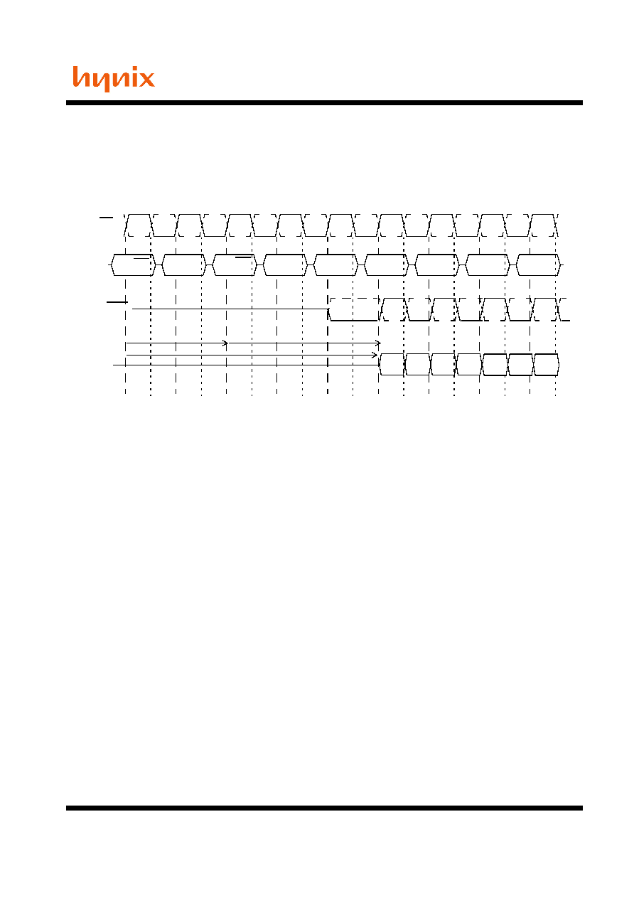
Burst Write Operation: RL = 5, WL = 4, tWR = 3 (AL=2, CL=3), BL = 4
t
DS
t
DS
t
DH
t
WPRE
t
WPST
t
DQSH
t
DQSL
DQS
DQS
D
DMin
DQS/
DQ
DM
t
DH
Data input (write) timing
DMin
DMin
DMin
D
D
D
DQS
CMD
NOP
NOP
NOP
NOP
NOP
NOP
DQs
NOP
CK/CK
T0
T2
T1
T3
T4
T5
T6
T7
Tn
WRITE A
Posted CAS
WL = RL - 1 = 4
DQS/DQS
< = t
DQSS
> = WR
DIN A
0
DIN A
1
DIN A
2
DIN A
3
Precharge
Completion of
the Burst Write

Rev 0.3 / May 2004
37
HY5PS56421(L)F
HY5PS56821(L)F
HY5PS561621(L)F
Burst Write Operation: RL = 3, WL = 2, tWR = 2 (AL=0, CL=3), BL = 4
Burst Write followed by Burst Read: RL = 5 (AL=2, CL=3), WL = 4, tWTR = 2, BL = 4
The minimum number of clock from the burst write command to the burst read command is [CL - 1 + BL/2 +
tWTR]. This tWTR is not a write recovery time (tWR) but the time required to transfer the 4bit write data from
the input buffer into sense amplifiers in the array. tWTR is defined in AC spec table of this data sheet.
CMD
NOP
NOP
NOP
NOP
Precharge
NOP
DQs
NOP
CK/CK
T0
T2
T1
T3
T4
T5
T6
T7
Tn
WRITE A
WL = RL - 1 = 2
DQS/
< = t
DQSS
> = WR
DIN A
0
DIN A
1
DIN A
2
DIN A
3
Bank A
Completion of
the Burst Write
Activate
> = tRP
DQS
CMD
NOP
NOP
NOP
NOP
DQ
CK/CK
T0
T2
T1
T3
T4
T5
T6
T7
T8
DIN A
0
DIN A
1
DIN A
2
DIN A
3
NOP
DQS/
DOUT A
0
WL = RL - 1 = 4
Post CAS
READ A
NOP
RL =5
AL = 2
CL = 3
NOP
NOP
Write to Read = CL - 1 + BL/2 + tWTR
> = tWTR
T9
DQS
DQS
DQS

Rev 0.3 / May 2004
38
HY5PS56421(L)F
HY5PS56821(L)F
HY5PS561621(L)F
Seamless Burst Write Operation: RL = 5, WL = 4, BL = 4
The seamless burst write operation is supported by enabling a write command every other clock for BL = 4
operation, every four clocks for BL = 8 operation. This operation is allowed regardless of same or different
banks as long as the banks are activated
CMD
NOP
NOP
NOP
NOP
NOP
NOP
DQ's
NOP
CK/CK
T0
T2
T1
T3
T4
T5
T6
T7
T8
DIN A
0
DIN A
1
DIN A
2
DIN A
3
Write A
Post CAS
WL = RL - 1 = 4
DQS/
Write B
Post CAS
DIN B
0
DIN B
1
DIN B
2
DIN B
3
DQS
DQS
DQS

Rev 0.3 / May 2004
39
HY5PS56421(L)F
HY5PS56821(L)F
HY5PS561621(L)F
Writes interrupted by a write
Burst write can only be interrupted by another write with 4 bit burst boundary. Any other case of write interrupt
is not allowed.
Write Burst Interrupt Timing Example: (CL=3, AL=0, RL=3, WL=2, BL=8)
Notes:
1. Write burst interrupt function is only allowed on burst of 8. Burst interrupt of 4 is prohibited.
2. Write burst of 8 can only be interrupted by another Write command. Write burst interruption by Read
command or Precharge command is prohibited.
3. Write burst interrupt must occur exactly two clocks after previous Write command. Any other Write burst
interrupt timings are prohibited.
4. Write burst interruption is allowed to any bank inside DRAM.
5. Write burst with Auto Precharge enabled is not allowed to interrupt.
6. Write burst interruption is allowed by another Write with Auto Precharge command.
7. All command timings are referenced to burst length set in the mode register. They are not referenced to
actual burst. For example, minimum Write to Precharge timing is WL+BL/2+tWR where tWR starts with
the rising clock after the un-interrupted burst end and not from the end of actual burst end.
CK/CK
CMD
DQS/DQS
DQs
NOP
NOP
NOP
NOP
NOP
NOP
NOP
NOP
A0
A1
A2
A3
B0
B1
B2
B3
B5
B6
B7
Write B
Write A
B4

Rev 0.3 / May 2004
40
HY5PS56421(L)F
HY5PS56821(L)F
HY5PS561621(L)F
2.5.5 Write Data Mask
One write data mask (DM) pin for each 8 data bits (DQ) will be supported on DDR2 SDRAMs, Consistent with
the implementation on DDR SDRAMs. It has identical timings on write operations as the data bits, and though
used in a uni-directional manner, is internally loaded identically to data bits to insure matched system timing.
DM of x4 and x16 bit organization is not used during read cycles. However DM of x8 bit organization can be
used as RDQS during read cycles by EMRS(1) settng.
Data Mask Timing
DQS/
DQ
DM
t
DS
t
DH
t
DS
t
DH
Write
CK
CK
COMMAND
DQS/DQS
DQ
DM
Case 2 : max t
DQSS
DQS/DQS
DQ
DM
t
DQSS
t
DQSS
t
WR
Data Mask Function, WL=3, AL=0, BL = 4 shown
Case 1 : min t
DQSS
DQS

Rev 0.3 / May 2004
41
HY5PS56421(L)F
HY5PS56821(L)F
HY5PS561621(L)F
2.6 Precharge Operation
The Precharge Command is used to precharge or close a bank that has been activated. The Precharge Com-
mand is triggered when CS, RAS and WE are low and CAS is high at the rising edge of the clock. The Pre-
charge Command can be used to precharge each bank independently or all banks simultaneously. Three
address bits A10, BA0 and BA1 for 512Mb are used to define which bank to precharge when the command is
issued.
Bank Selection for Precharge by Address Bits
Burst Read Operation Followed by Precharge
Minium Read to precharge command spacing to the same bank = AL + BL/2 clocks
For the earliest possible precharge, the precharge command may be issued on the rising edge which is
"Additive latency(AL) + BL/2 clocks" after a Read command. A new bank active (command) may be issued to
the same bank after the RAS precharge time (t
RP
). A precharge command cannot be issued until t
RAS
is sat-
isfied.
The minimum Read to Precharge spacing has also to satisfy a minimum analog time from the rising clock
egde that initiates the last 4-bit prefetch of a Read to Precharge command. This time is called tRTP (Read to
Precharge). For BL = 4 this is the time from the actual read (AL after the Read command) to Precharge com-
mand. For BL = 8 this is the time from AL + 2 clocks after the Read to the Precharge command.
A10
BA1
BA0
Precharged Bank(s)
Remarks
LOW
LOW
LOW
Bank 0 only
LOW
LOW
HIGH
Bank 1 only
LOW
HIGH
LOW
Bank 2 only
LOW
HIGH
HIGH
Bank 3 only
HIGH
DON'T CARE
DON'T CARE
All Banks

Rev 0.3 / May 2004
42
HY5PS56421(L)F
HY5PS56821(L)F
HY5PS561621(L)F
Example 1: Burst Read Operation Followed by Precharge:
RL = 4, AL = 1, CL = 3, BL = 4, t
RTP
<= 2 clocks
Example 2: Burst Read Operation Followed by Precharge:
RL = 4, AL = 1, CL = 3, BL = 8, t
RTP
<= 2 clocks
CMD
NOP
NOP
Precharge
NOP
DQ's
NOP
CK/CK
DOUT A
0
DOUT A
1
DOUT A
2
DOUT A
3
READ A
Post CAS
RL =4
DQS/DQS
Active
Bank A
> = t
RP
NOP
CL =3
NOP
> = t
RAS
T0
T2
T1
T3
T4
T5
T6
T7
T 8
AL + BL/2 clks
AL = 1
CL = 3
> = t
RTP
CMD
NOP
NOP
NOP
NOP
DQ's
NOP
CK/CK
DOUT A
0
DOUT A
1
DOUT A
2
DOUT A
3
READ A
Post CAS
RL =4
DQS/DQS
Precharge A
NOP
T0
T2
T1
T3
T4
T5
T6
T7
T 8
AL + BL/2 clks
AL = 1
CL = 3
> = t
RTP
DOUT A
4
DOUT A
5
DOUT A
6
DOUT A
7
first 4-bit prefetch
second 4-bit prefetch
NOP

Rev 0.3 / May 2004
43
HY5PS56421(L)F
HY5PS56821(L)F
HY5PS561621(L)F
Example 3: Burst Read Operation Followed by Precharge:
RL = 5, AL = 2, CL = 3, BL = 4, t
RTP
<= 2 clocks
Example 4: Burst Read Operation Followed by Precharge:
RL = 6, AL = 2, CL = 4, BL = 4, t
RTP
<= 2 clocks
CMD
NOP
NOP
NOP
NOP
DQ's
Precharge A
CK/CK
DOUT A
0
DOUT A
1
DOUT A
2
DOUT A
3
READ A
Posted CAS
AL = 2
CL =3
RL =5
DQS/DQS
Activate
Bank A
> = t
RP
NOP
CL =3
NOP
> = t
RAS
T0
T2
T1
T3
T4
T5
T6
T7
T 8
AL + BL/2 clks
> = t
RTP
CMD
NOP
NOP
NOP
NOP
DQ's
Precharge A
CK/CK
DOUT A
0
DOUT A
1
DOUT A
2
DOUT A
3
READ A
Post CAS
AL = 2
CL =4
RL = 6
DQS/DQS
Activate
Bank A
> = t
RP
NOP
CL =4
NOP
> = t
RAS
T0
T2
T1
T3
T4
T5
T6
T7
T 8
AL + BL/2 Clks
> = t
RTP

Rev 0.3 / May 2004
44
HY5PS56421(L)F
HY5PS56821(L)F
HY5PS561621(L)F
Example 5: Burst Read Operation Followed by Precharge:
RL = 4, AL = 0, CL = 4, BL = 8, t
RTP
> 2 clocks
CMD
NOP
NOP
NOP
NOP
DQ's
Precharge A
CK/CK
DOUT A
0
DOUT A
1
DOUT A
2
DOUT A
3
READ A
Post CAS
AL = 0
CL =4
RL = 4
DQS/DQS
Activate
Bank A
> = t
RP
NOP
NOP
> = t
RAS
T0
T2
T1
T3
T4
T5
T6
T7
T 8
AL + 2 Clks + max{tRTP;2 tCK}*
* : rounded to next interger
DOUT A
4
DOUT A
5
DOUT A
6
DOUT A
7
first 4-bit prefetch
second 4-bit prefetch
> = t
RTP

Rev 0.3 / May 2004
45
HY5PS56421(L)F
HY5PS56821(L)F
HY5PS561621(L)F
Burst Write followed by Precharge
Minium Write to Precharge Command spacing to the same bank = WL + BL/2 clks + tWR
For write cycles, a delay must be satisfied from the completion of the last burst write cycle until the Precharge
Command can be issued. This delay is known as a write recovery time (tWR) referenced from the completion
of the burst write to the precharge command. No Precharge command should be issued prior to the tWR delay.
Example 1: Burst Write followed by Precharge: WL = (RL-1) =3
Example 2: Burst Write followed by Precharge: WL = (RL-1) = 4
CMD
NOP
NOP
NOP
NOP
NOP
NOP
DQs
NOP
CK/CK
T0
T2
T1
T3
T4
T5
T6
T7
T 8
DIN A
0
DIN A
1
DIN A
2
DIN A
3
WRITE A
Posted CAS
WL = 3
DQS/DQS
> =
WR
Precharge A
Completion of the Burst Write
CMD
NOP
NOP
NOP
NOP
NOP
NOP
DQs
NOP
CK/CK
T0
T2
T1
T3
T4
T5
T6
T7
T 9
DIN A
0
DIN A
1
DIN A
2
DIN A
3
WRITE A
Posted CAS
WL = 4
DQS/DQS
> = t
WR
Precharge A
Completion of the Burst Write

Rev 0.3 / May 2004
46
HY5PS56421(L)F
HY5PS56821(L)F
HY5PS561621(L)F
2.7 Auto Precharge Operation
Before a new row in an active bank can be opened, the active bank must be precharged using either the Pre-
charge command or the auto-precharge function. When a Read or a Write command is given to the DDR2
SDRAM, the CAS timing accepts one extra address, column address A10, to allow the active bank to auto-
matically begin precharge at the earliest possible moment during the burst read or write cycle. If A10 is low
when the READ or WRITE command is issued, then normal Read or Write burst operation is executed and
the bank remains active at the completion of the burst sequence. If A10 is high when the Read or Write com-
mand is issued, then the auto-precharge function is engaged. During auto-precharge, a Read command will
execute as normal with the exception that the active bank will begin to precharge on the rising edge which is
CAS latency (CL) clock cycles before the end of the read burst.
Auto-precharge is also implemented during Write commands. The precharge operation engaged by the Auto
precharge command will not begin until the last data of the burst write sequence is properly stored in the
memory array.
This feature allows the precharge operation to be partially or completely hidden during burst read cycles
(dependent upon CAS latency) thus improving system performance for random data access. The RAS lock-
out circuit internally delays the Precharge operation until the array restore operation has been completed
(tRAS satisfied) so that the auto precharge command may be issued with any read or write command.
Burst Read with Auto Precharge
If A10 is high when a Read Command is issued, the Read with Auto-Precharge function is engaged. The
DDR2 SDRAM starts an Auto Precharge operation on the rising edge which is (AL + BL/2) cycles later than
the read with AP command if tRAS(min) and tRTP are satisfied.
If tRAS(min) is not satisfied at the edge, the start point of auto-precharge operation will be delayed until
tRAS(min) is satisfied.
If tRTP(min) is not satisfied at the edge, the start point of auto-precharge operation will be delayed until
tRTP(min) is satisfied.
In case the internal precharge is pushed out by tRTP, tRP starts at the point where the internal precharge
happens (not at the next rising clock edge after this event). So for BL = 4 the minimum time from Read_AP to
the next Activate command becomes AL + (tRTP + tRP)* (see example 2) for BL = 8 the time from Read_AP
to the next Activate is AL + 2 + (tRTP + tRP)*, where "*" means: "rounded up to the next integer". In any event
internal precharge does not start earlier than two clocks after the last 4-bit prefetch.
A new bank activate (command) may be issued to the same bank if the following two conditions are satisfied
simultaneously.
(1) The RAS precharge time (tRP) has been satisfied from the clock at which the auto precharge begins.
(2) The RAS cycle time (tRC) from the previous bank activation has been satisfied.

Rev 0.3 / May 2004
47
HY5PS56421(L)F
HY5PS56821(L)F
HY5PS561621(L)F
Example 1: Burst Read Operation with Auto Precharge:
RL = 4, AL = 1, CL = 3, BL = 8, t
RTP
<= 2 clocks
Example 2: Burst Read Operation with Auto Precharge:
RL = 4, AL = 1, CL = 3, BL = 4, t
RTP
> 2 clocks
CMD
NOP
NOP
NOP
NOP
DQ's
NOP
CK/CK
DOUT A
0
DOUT A
1
DOUT A
2
DOUT A
3
READ A
Post CAS
RL =4
DQS/DQS
T0
T2
T1
T3
T4
T5
T6
T7
T 8
AL + BL/2 clks
AL = 1
CL = 3
> = t
RTP
DOUT A
4
DOUT A
5
DOUT A
6
DOUT A
7
first 4-bit prefetch
second 4-bit prefetch
NOP
t
RTP
NOP
Precharge begins here
Activate
Bank A
> = t
RP
Autoprecharge
CMD
NOP
NOP
NOP
NOP
DQ's
NOP
CK/CK
DOUT A
0
DOUT A
1
DOUT A
2
DOUT A
3
READ A
Post CAS
RL =4
DQS/DQS
T0
T2
T1
T3
T4
T5
T6
T7
T 8
> = AL + tRTP + tRP
AL = 1
CL = 3
4-bit prefetch
NOP
t
RTP
NOP
Precharge begins here
Activate
Bank A
Autoprecharge
t
RP

Rev 0.3 / May 2004
48
HY5PS56421(L)F
HY5PS56821(L)F
HY5PS561621(L)F
Example 3: Burst Read with Auto Precharge Followed by an activation to the Same
Bank(tRC Limit):
RL = 5 (AL = 2, CL = 3, internal tRCD = 3, BL = 4, t
RTP
<= 2 clocks)
Example 4: Burst Read with Auto Precharge Followed by an Activation to the Same
Bank(tRP Limit):
RL = 5 (AL = 2, CL = 3, internal tRCD = 3, BL = 4, t
RTP
<= 2 clocks)
CMD
NOP
NOP
NOP
NOP
NOP
DQ's
NOP
CK/CK
T0
T2
T1
T3
T4
T5
T6
T7
T8
DOUT A
0
DOUT A
1
DOUT A
2
DOUT A
3
READ A
Post CAS
AL = 2
CL =3
RL = 5
DQS/DQS
Activate
Bank A
> = t
RP
A10 = 1
Auto Precharge Begins
CL =3
> = t
RC
NOP
> = tRAS(min)
CMD
NOP
NOP
NOP
NOP
NOP
DQ's
NOP
CK/CK
T0
T2
T1
T3
T4
T5
T6
T7
T8
DOUT A
0
DOUT A
1
DOUT A
2
DOUT A
3
READ A
Post CAS
AL = 2
CL =3
RL = 5
DQS/DQS
Activate
Bank A
> = t
RP
A10 = 1
Auto Precharge Begins
CL =3
> = t
RC
NOP
> = tRAS(min)

Rev 0.3 / May 2004
49
HY5PS56421(L)F
HY5PS56821(L)F
HY5PS561621(L)F
Burst Write with Auto-Precharge
If A10 is high when a Write Command is issued, the Write with Auto-Precharge function is engaged. The
DDR2 SDRAM automatically begins precharge operation after the completion of the burst write plus write
recovery time (tWR). The bank undergoing auto-precharge from the completion of the write burst may be
reactivated if the following two conditions are satisfied.
(1) The data-in to bank activate delay time (WR + tRP) has been satisfied.
(2) The RAS cycle time (tRC) from the previous bank activation has been satisfied.
Burst Write with Auto-Precharge (tRC Limit): WL = 2, tWR =2, BL = 4, tRP=3
Burst Write with Auto-Precharge (tWR + tRP): WL = 4, tWR =2, BL = 4, tRP=3
CMD
NOP
NOP
NOP
NOP
NOP
Bank A
DQs
NOP
CK/CK
T0
T2
T1
T3
T4
T5
T6
T7
Tm
DIN A
0
DIN A
1
DIN A
2
DIN A
3
WRA BankA
Post CAS
WL =RL - 1 = 2
DQS/DQS
A10 = 1
Auto Precharge Begins
NOP
> =
WR
Completion of the Burst Write
Active
> = t
RP
> = t
RC
CMD
NOP
NOP
NOP
NOP
NOP
Bank A
DQs
NOP
CK/CK
T0
T4
T3
T5
T6
T7
T8
T9
T12
DIN A
0
DIN A
1
DIN A
2
DIN A
3
WRA Bank A
Post CAS
WL =RL - 1 = 4
DQS/DQS
A10 = 1
Auto Precharge Begins
NOP
> =
WR
Completion of the Burst Write
Active
> = t
RP
> = t
RC

Rev 0.3 / May 2004
50
HY5PS56421(L)F
HY5PS56821(L)F
HY5PS561621(L)F
2.8 Refresh Commands
DDR2 SDRAMs require a refresh of all rows in any rolling 64 ms interval. Each refresh is generated in one of
two ways: by an explicit Auto-Refresh command, or by an internally timed event in SELF REFRESH mode.
Dividing the number of device rows into the rolling 64ms interval, tREFI, which is a guideline to controllers for
distributed refresh timing. For example, a 512Mb DDR2 SDRAM has 8192 rows resulting in a tREFI of 7.8.
To avoid excessive interruptions to the memory controller, higher density DDR2 SDRAMS maintain 7.8
average refresh time and perform multiple internal refresh bursts. In these cases, the refresh recovery times,
tRFC an tXSNR are extended to accomodate these internal operations.
2.8.1 Auto Refresh Command
AUTO REFRESH is used during normal operation of the DDR2 SDRAM. This command is nonpersistent, so it
must be issued each time a refresh is required. The refresh addressing is generated by the internal refresh
controller. This makes the address bits "Don't Care" during an AUTO REFRESH command.
When CS, RAS and CAS are held low and WE high at the rising edge of the clock, the chip enters the Refresh
mode (REF). All banks of the DDR2 SDRAM must be precharged and idle for a minimum of the Precharge
time (tRP) before the Refresh command (REF) can be applied. An address counter, internal to the device,
supplies the bank address during the refresh cycle. No control of the external address bus is required once
this cycle has started.
When the refresh cycle has completed, all banks of the DDR2 SDRAM will be in the precharged (idle) state. A
delay between the Refresh command (REF) and the next Activate command or subsequent Refresh com-
mand must be greater than or equal to the Refresh cycle time (tRFC).
To allow for improved efficiency in scheduling andswitching between tasks, some flexibility in the absolute
refresh interval is provided. A maximum of eight Refresh commands can be posted to any given DDR2
SDRAM, meaning that the maximum absolute interval between any Refresh command and the next Refresh
command is 9 * tREFI.
2.8.2 Self Refresh Operation
The Self Refresh command can be used to retain data in the DDR2 SDRAM, even if the rest of the system is
powered down. When in the Self Refresh mod, the DDR2 SDRAM retains data without external clocking.
The DDR2 SDRAM device has a built-in timer to accommodate Self Refresh operation. The Self Refresh
Command is defined by having CS, RAS, CAS and CKE held low with WE high at the rising edge of the clock.
ODT must be turned off before issuing Self Refresh command, by either driving ODT pin low or using EMRS
command. Once the Command is registered, CKE must be held low to keep the device in Self Refresh mode.
The DLL is automatically disabled upon entering Self Refresh and is automatically enabled upon existing Self
Refresh. When the DDR2 SDRAM has entered Self Refresh mode all of the external signals
except CKE, are
"don't care". The DRAM initiates a minimum of one Auto Refresh command internally within tCKE period once
it enters Self Refresh mode.The clock is internally disabled during Self Refresh Operation to save power. The
minimum time that the DDR2 SDRAM must remain in Self Refresh mode is tCKE. The user may change the
external clock frequency or halt the external clock one clock after Self-Refresh entry is registered, however,
the clock must be restarted and stable before the device can exit Self Refresh operation.
CMD
NOP
REF
REF
NOP
ANY
CK/CK
T0
T2
T1
T3
Tm
Tn
Tn + 1
Precharge
CKE
NOP
> = t
RP
> = t
RFC
> = t
RFC
High

Rev 0.3 / May 2004
51
HY5PS56421(L)F
HY5PS56821(L)F
HY5PS561621(L)F
The procedure for existing Self Refresh requires a sequence of commands. First, the clock must be stable
prior to CKE going back HIGH. Once Self Refresh Exit command is registered, a delay equal or longer than
the tXSNR or tXSRD must be satisfied before a valid command can be issued to the device. CKE must
remain high for the entire Self Refresh exit period tXSRD for proper operation. Upon exit from Self Refresh,
the DDR2 SDRAM can be put back into Self Refresh mode after tXSRD expires.NOP or deselect commands
must be registered on each positive clock edge during the Self Refresh exit interval. ODT should also be
turned off during tXSRD.
The Use of Self Refresh mode introduce the possibility that an internally timed refresh event can be missed
when CKE is raised for exit from Self Refresh mode. Upon exit from Self Refresh, the DDR2 SDRAM requires
a minimum of one extra auto refresh command before it is put back into Self Refresh mode.
- Device must be in the "All banks idle" state prior to entering Self Refresh mode.
- ODT must be turned off tAOFD before entering Self Refresh mode, and can be turned on again
when tXSRD timing is satisfied.
- tXSRD is applied for a Read or a Read with autoprecharge command
- tXSNR is applied for any command except a Read or a Read with autoprecharge command.
CMD
CK
T0
T2
T1
Tm
Tn
CKE
T3
T4
T5
ODT
Self
Refresh
T6
NOP
tAOFD
CK
> = tXSNR
> = tXSRD
tRP*
Valid
tCK
tCH tCL
tIS
tIS
tIS
tIS tIH
NOP
NOP

Rev 0.3 / May 2004
52
HY5PS56421(L)F
HY5PS56821(L)F
HY5PS561621(L)F
2.9 Power-Down
Power-down is synchronously entered when CKE is registered low (along with Nop or Deselect command). CKE
is not allowed to go low while mode register or extended mode register command time, or read or write operation
is in progress. CKE is allowed to go low while any of other operations such as row activation, precharge or auto-
precharge, or auto-refresh is in progress, but power-down IDD spec will not be applied until finishing those opera-
tions. Timing diagrams are shown in the following pages with details for entry into power down.
The DLL should be in a locked state when power-down is entered. Otherwise DLL should be reset after exiting
power-down mode for proper read operation.
If power-down occurs when all banks are idle, this mode is referred to as precharge power-down; if power-down
occurs when there is a row active in any bank, this mode is referred to as active power-down. Entering power-
down deactivates the input and output buffers, excluding CK, CK, ODT and CKE. Also the DLL is disabled upon
entering precharge power-down or slow exit active power-down, but the DLL is kept enabled during fast exit
active power-down. In power-down mode, CKE low and a stable clock signal must be maintained at the inputs of
the DDR2 SDRAM, and ODT should be in a valid state but all other input signals are "Don't Care". CKE low must
be maintained until tCKE has been satisfied. Power-down duration is limited by 9 times tREFI of the device.
The power-down state is synchronously exited when CKE is registered high (along with a Nop or Deselect com-
mand). CKE high must be maintained until tCKE has been satisfied. A valid, executable command can be applied
with power-down exit latency, tXP, tXARD, or tXARDS, after CKE goes high. Power-down exit latency is defined
at AC spec table of this data sheet.
Basic Power Down Entry and Exit timing diagram
t
IS
t
IS
CK/CK
CKE
Command
VALID
NOP
VALID
Don't Care
NOP
t
XP,
t
XARD,
Enter Power-Down mode
t
CKE
t
IH
t
IH
t
CKE
t
XARDS
VALID
t
IH
Exit Power-Down mode
t
IS
t
IH
t
CKE
t
IH
VALID
t
IS

Rev 0.3 / May 2004
53
HY5PS56421(L)F
HY5PS56821(L)F
HY5PS561621(L)F
CK
CMD
CKE
DQ
DQS
CMD
CKE
DQ
DQS
CMD
CKE
DQ
DQS
CMD
CKE
DQ
DQS
RDA
RDA
BL=8
PRE
PRE
AL + BL/2
with tRTP = 7.5ns
& tRAS min satisfied
AL + BL/2
with tRTP = 7.5ns
& tRAS min satisfied
Read to power down entry
Read with Autoprecharge to power down entry
CK
CK
CK
Start internal precharge
AL + CL
AL + CL
CKE should be kept high until the end of burst operation.
AL + CL
BL=4
CKE should be kept high
CKE should be kept high
until the end of burst operation.
AL + CL
T0
Tx
Tx+2
Tx+3
Tx+4
Tx+5
Tx+6
T1
T2
Tx+1
Tx+7
Tx+8
Tx+9
Q
Q
Q
Q
Q
Q
Q
Q
Q
Q
Q
Q
CKE should be kept high until the end of burst operation.
until the end of burst operation.
Q
Q
Q
Q
Q
Q
Q
Q
RD
BL=4
RD
BL=8
Read operation starts with a read command and
Q
Q
Q
Q
T0
Tx
Tx+2
Tx+3
Tx+4
Tx+5
Tx+6
T1
T2
Tx+1
Tx+7
Tx+8
Tx+9
T0
Tx
Tx+2
Tx+3
Tx+4
Tx+5
Tx+6
T1
T2
Tx+1
Tx+7
Tx+8
Tx+9
T0
Tx
Tx+2
Tx+3
Tx+4
Tx+5
Tx+6
T1
T2
Tx+1
Tx+7
Tx+8
Tx+9
DQS
DQS
DQS
DQS

Rev 0.3 / May 2004
54
HY5PS56421(L)F
HY5PS56821(L)F
HY5PS561621(L)F
CMD
CKE
DQ
DQS
CMD
CKE
DQ
DQS
T0
Tm+1
Tm+3
Tx
Tx+1
Tx+2
Ty
T1
Tm
Tm+2
Ty+1
Ty+2
Ty+3
WR
WR
BL=8
CMD
CKE
DQ
DQS
CMD
CKE
DQ
DQS
T0
Tm+1
Tm+3
Tx
Tx+1
Tx+2
Tx+3
T1
Tm
Tm+2
Tx+4
Tx+5
Tx+6
WRA
WRA
BL=8
PRE
PRE
D
D
D
D
D
D
D
D
D
D
D
D
tWTR
tWTR
WR*1
D
D
D
D
D
D
D
D
D
D
D
D
WR*1
Write to power down entry
Write with Autoprecharge to power down entry
CK
CK
CK
CK
WL
BL=4
BL=4
WL
WL
WL
T0
Tm+1
Tm+3
Tm+4
Tm+5
Tx
Tx+1
T1
Tm
Tm+2
Tx+2
Tx+3
Tx+4
CK
CK
* 1: WR is programmed through MRS
T0
Tm+1
Tm+3
Tm+4
Tm+5
Tx
Tx+1
T1
Tm
Tm+2
Tx+2
Tx+3
Tx+4
DQS
DQS
DQS
DQS

Rev 0.3 / May 2004
55
HY5PS56421(L)F
HY5PS56821(L)F
HY5PS561621(L)F
CMD
CKE
CMD
CKE
T0
T3
T5
T6
T7
T8
T9
T1
T2
T4
T10
CMD
CKE
CMD
CKE
CKE can go to low one clock after an Active command
PR or
MRS or
PRA
EMRS
REF
ACT
tMRD
Refresh command to power down entry
Active command to power down entry
Precharge/Precharge all command to power down entry
MRS/EMRS command to power down entry
CK
CK
CKE can go to low one clock after a Precharge or Precharge all command
CKE can go to low one clock after an Auto-refresh command
T11

Rev 0.3 / May 2004
56
HY5PS56421(L)F
HY5PS56821(L)F
HY5PS561621(L)F
2. 10 Asynchronous CKE Low Event
DRAM requires CKE to be maintained "HIGH" for all valid operations as defined in this data sheet. If CKE asyn-
chronously drops "LOW" during any valid operation DRAM is not guaranteed to preserve the contents of array. If
this event occurs, memory controller must satisfy DRAM timing specification tDelay before turning off the clocks.
Stable clocks must exist at the input of DRAM before CKE is raised "HIGH" again. DRAM must be fully re-initial-
ized (steps 4 thru 13) as described in initializaliation sequence. DRAM is ready for normal operation after the ini-
tialization sequence. See AC timing parametric table for tDelay specification
tCK
CK
CK#
tDelay
CKE
CKE asynchronously drops low
Clocks can be turned
off after this point
Stable clocks

Rev 0.3 / May 2004
57
HY5PS56421(L)F
HY5PS56821(L)F
HY5PS561621(L)F
Input Clock Frequency Change during Precharge Power Down
DDR2 SDRAM input clock frequency can be changed under following condition:
DDR2 SDRAM is in precharged power down mode. ODT must be turned off and CKE must be at logic LOW level.
A minimum of 2 clocks must be waited after CKE goes LOW before clock frequency may change. SDRAM input
clock frequency is allowed to change only within minimum and maximum operating frequency specified for the
particular speed grade. During input clock frequency change, ODT and CKE must be held at stable LOW levels.
Once input clock frequency is changed, stable new clocks must be provided to DRAM before precharge power
down may be exited and DLL must be RESET via EMRS after precharge power down exit. Depending on new
clock frequency an additional MRS command may need to be issued to appropriately set the WR, CL etc.. During
DLL re-lock period, ODT must remain off. After the DLL lock time, the DRAM is ready to operate with new clock
frequency.
CK
CKE
T0
T4
Tx+1
Ty
Ty+1
Ty+2
T1
T2
Tx
CK
Valid
DLL
NOP
200 Clocks
Frequency Change
Ty+3
Tz
NOP
NOP
NOP
NOP
RESET
tRP
Clock Frequency Change in Precharge Power Down Mode
tXP
Occurs here
tAOFD
Stable new clock
before power down exit
ODT is off during
DLL RESET
Minmum 2 clocks
required before
changing frequency
ODT
CMD
Ty+4

Rev 0.3 / May 2004
58
HY5PS56421(L)F
HY5PS56821(L)F
HY5PS561621(L)F
2.11 No Operation Command
The No Operation command should be used in cases when the DDR2 SDRAM is in an idle or a wait state.
The purpose of the No Operation command (NOP) is to prevent the DDR2 SDRAM from registering any
unwanted commands between operations. A No Operation command is registered when CS is low with RAS,
CAS, and WE held high at the rising edge of the clock. A No Operation command will not terminate a previous
operation that is still executing, such as a burst read or write cycle.
2.12 Deselect Command
The Deselect command performs the same function as a No Operation command. Deselect command occurs
when CS is brought high at the rising edge of the clock, the RAS, CAS, and WE signals become don't cares.

Rev 0.3 / May 2004
59
HY5PS56421(L)F
HY5PS56821(L)F
HY5PS561621(L)F
3. Truth Tables
3.1 Command truth table.
Function
CKE
CS
RAS
CAS
WE
BA0
BA1
BA2
A15-A11 A10
A9 - A0
Notes
Previous
Cycle
Current
Cycle
(Extended) Mode Register Set
H
H
L
L
L
L
BA
OP Code
1,2
Refresh (REF)
H
H
L
L
L
H
X
X
X
X
1
Self Refresh Entry
H
L
L
L
L
H
X
X
X
X
1
Self Refresh Exit
L
H
H
X
X
X
X
X
X
X
1,7
L
H
H
H
Single Bank Precharge
H
H
L
L
H
L
BA
X
L
X
1,2
Precharge all Banks
H
H
L
L
H
L
X
X
H
X
1
Bank Activate
H
H
L
L
H
H
BA
Row Address
1,2
Write
H
H
L
H
L
L
BA
Column
L
Column
1,2,3,
Write with Auto Precharge
H
H
L
H
L
L
BA
Column
H
Column
1,2,3,
Read
H
H
L
H
L
H
BA
Column
L
Column
1,2,3
Read with Auto-Precharge
H
H
L
H
L
H
BA
Column
H
Column
1,2,3
No Operation
H
X
L
H
H
H
X
X
X
X
1
Device Deselect
H
X
H
X
X
X
X
X
X
X
1
Power Down Entry
H
L
H
X
X
X
X
X
X
X
1,4
L
H
H
H
Power Down Exit
L
H
H
X
X
X
X
X
X
X
1,4
L
H
H
H
1. All DDR2 SDRAM commands are defined by states of CS, RAS, CAS , WE and CKE at the rising edge of the clock.
2. Bank addesses BA0, BA1, BA2 (BA) determine which bank is to be operated upon. For (E)MRS BA selects an (Extended) Mode
Register.
3. Burst reads or writes at BL=4 cannot be terminated or interrupted. See sections "Reads interrupted by a Read" and "Writes inter-
rupted by a Write" in section 2.2.4 for details.
4. The Power Down Mode does not perform any refresh operations. The duration of Power Down is therefore limited by the refresh
requirements outlined in section 2.2.7.
5. The state of ODT does not affect the states described in this table. The ODT function is not available during Self Refresh. See
section 2.2.2.4.
6. "X" means "H or L (but a defined logic level)".
7. Self refresh exit is asynchronous.

Rev 0.3 / May 2004
60
HY5PS56421(L)F
HY5PS56821(L)F
HY5PS561621(L)F
3.2 Clock Enable (CKE) Truth Table for Synchronous Transitions
Current State
2
CKE
Command (N)
3
RAS, CAS, WE, CS
Action (N)
3
Notes
Previous Cycle
1
(N-1)
Current Cycle
1
(N)
Power Down
L
L
X
Maintain Power-Down
11, 13, 15
L
H
DESELECT or NOP
Power Down Exit
4, 8, 11,13
Self Refresh
L
L
X
Maintain Self Refresh
11, 15
L
H
DESELECT or NOP
Self Refresh Exit
4, 5,9
Bank(s) Active
H
L
DESELECT or NOP
Active Power Down Entry
4,8,10,11,13
All Banks Idle
H
L
DESELECT or NOP
Precharge Power Down Entry
4, 8, 10,11,13
H
L
REFRESH
Self Refresh Entry
6, 9, 11,13
H
H
Refer to the Command Truth Table
7
Notes:
1. CKE (N) is the logic state of CKE at clock edge N; CKE (N�1) was the state of CKE at the previous clock edge.
2. Current state is the state of the DDR SDRAM immediately prior to clock edge N.
3. COMMAND (N) is the command registered at clock edge N, and ACTION (N) is a result of COMMAND (N).
4. All states and sequences not shown are illegal or reserved unless explicitely described elsewhere in this document.
5. On Self Refresh Exit DESELECT or NOP commands must be issued on every clock edge occurring during the t
XSNR
period.
Read commands may be issued only after t
XSRD
(200 clocks) is satisfied.
6. Self Refresh mode can only be entered from the All Banks Idle state.
7. Must be a legal command as defined in the Command Truth Table.
8. Valid commands for Power Down Entry and Exit are NOP and DESELECT only.
9. Valid commands for Self Refresh Exit are NOP and DESELECT only.
10. Power Down and Self Refresh can not be entered while Read or Write operations, (Extended) Mode Register Set operations or
Precharge operations are in progress. See section 2.2.9 "Power Down" and 2.2.8 "Self Refresh Command" for a detailed list of
restrictions.
11. Minimum CKE high time is three clocks.; minimum CKE low time is three clocks.
12. The state of ODT does not affect the states described in this table. The ODT function is not available during Self Refresh. See
section 2.2.2.4.
13. The Power Down does not perform any refresh operations. The duration of Power Down Mode is therefore limited by the refresh
requirements outlined in section 2.2.7.
14. CKE must be maintained high while the SDRAM is in OCD calibration mode .
15. "X" means "don't care (including floating around VREF)" in Self Refresh and Power Down. However ODT must be driven high or
low in Power Down if the ODT fucntion is enabled (Bit A2 or A6 set to "1" in EMRS(1) ).
3.3 Data Mask Truth Table
Name (Functional)
DM
DQs
Note
Write enable
L
Valid
1
Write inhibit
H
X
1
1. Used to mask write data, provided coinsident with the corresponding data

Rev 0.3 / May 2004
61
HY5PS56421(L)F
HY5PS56821(L)F
HY5PS561621(L)F
4.1 Absolute Maximum DC Ratings
4.2 Operating Temperature Condition
Symbol
Parameter
Rating
Units
Notes
VDD
Voltage on VDD pin relative to Vss
- 1.0 V ~ 2.3 V
V
1
VDDQ
Voltage on VDDQ pin relative to Vss
- 0.5 V ~ 2.3 V
V
1
VDDL
Voltage on VDDL pin relative to Vss
- 0.5 V ~ 2.3 V
V
1
V
IN
,
V
OUT
Voltage on any pin relative to Vss
- 0.5 V ~ 2.3 V
V
1
T
STG
Storage Temperature
-55 to +100
�C 1
1.
Stresses greater than those listed under "Absolute Maximum Ratings" may cause permanent damage to the device. This is a
stress rating only and functional operation of the device at these or any other conditions above those indicated in the operational
sections of this specification is not implied. Exposure to absolute maximum rating conditions for extended periods may affect reli-
ability.
Symbol
Parameter
Rating
Units
Notes
Toper
Operating Temperature
0 to 85
�C 1,2
1. Operating Temperature is the case surface temperature on the center/top side of the DRAM. For the measurement conditions,
please refer to JESD51-2 standard.
2. The operatin temperature range are the temperature where all DRAM specification will be supported. Outside of this temperature
rang, even it is still within the limit of stress condition, some deviation on portion of operation specification may be required. During
operation, the DRAM case temperature must be maintained between 0 ~ 85�C under all other specification parameters. However,
in some applications, it is desirable to operate the DRAM up to 95�C case temperature. Therefore 2 spec options may exist.
1) Supporting 0 - 85�C with full JEDEC AC & DC specifications. This is the minimum requirements for all oprating tempera-
ture options.
2) Supporting 0 - 85�C and being able to extend to 95�C with doubling auto-refresh commands in frequency to a 32 ms
period(tRFI=3.9us).
Note; Self-refresh period within the above DRAM is hard coded at 64ms(tREFI= 7.8us). Therfore, it is imperative that the sys-
tem ensures the DRAM is at or below 85�C case temperature before initiating self-refresh operation.
4. Operating Conditions

Rev 0.3 / May 2004
62
HY5PS56421(L)F
HY5PS56821(L)F
HY5PS561621(L)F
5.1 DC Operation Conditions
5.1.1 Recommended DC Operating Conditions (SSTL_1.8)
5.1.2 ODT DC electrical characteristics
Note 1: Test condition for Rtt measurements
Measurement Definition for Rtt(eff):
Apply V
IH
(ac) and V
IL
(ac) to test pin separately, then measure current I(V
IH
(ac)) and I( V
IL
(ac)) respectively. V
IH
(ac), V
IL
(ac), and VDDQ values defined in SSTL_18
Measurement Definition for VM : Measurement Voltage at test pin(mid point) with no load.
Symbol
Parameter
Rating
Units
Notes
Min.
Typ.
Max.
VDD
Supply Voltage
1.7
1.8
1.9
V
VDDL
Supply Voltage for DLL
1.7
1.8
1.9
V
4
VDDQ
Supply Voltage for Output
1.7
1.8
1.9
V
4
VREF
Input Reference Voltage
0.49*VDDQ
0.50*VDDQ
0.51*VDDQ
mV
1, 2
VTT
Termination Voltage
V
REF
-0.04
V
REF
V
REF
+0.04
V
3
There is no specific device VDD supply voltage requirement for SSTL-1.8 compliance. However under all conditions VDDQ must
be less than or equal to VDD.
1. The value of VREF may be selected by the user to provide optimum noise margin in the system. Typically the value of VREF is
expected to be about 0.5 x VDDQ of the transmitting device and VREF is expected to track variations in VDDQ.
2. Peak to peak ac noise on VREF may not exceed +/-2% VREF (dc).
3. VTT of transmitting device must track VREF of receiving device.
4. VDDQ tracks with VDD, VDDL tracks with VDD. AC parameters are measured with VDD, VDDQ and VDDDL tied together
PARAMETER/CONDITION
SYMBOL
MIN
NOM
MAX
UNITS NOTES
Rtt effective impedance value for EMRS(A6,A2)=0,1; 75 ohm
Rtt1(eff)
60
75
90
ohm
1
Rtt effective impedance value for EMRS(A6,A2)=1,0; 150 ohm
Rtt2(eff)
120
150
180
ohm
1
Deviation of V
M
with respect to VDDQ/2
delta VM -3.75
+3.75
%
1
delta VM =
2 x Vm
VDDQ
x 100%
- 1
Rtt(eff) =
V
IH
(ac)
-
V
IL
(ac)
I(
V
IH
(ac)
) - I(
V
IL
(ac)
)
5. AC & DC Operating Conditons

Rev 0.3 / May 2004
63
HY5PS56421(L)F
HY5PS56821(L)F
HY5PS561621(L)F
5.2.1 Input DC Logic Leve
l
5.2.2 Input AC Logic Level
5.2.3 AC Input Test Conditions
Notes:
1.
Input waveform timing is referenced to the input signal crossing through the V
REF
level applied to the device under test.
2.
The input signal minimum slew rate is to be maintained over the range from V
IL(dc)
max to V
IH(ac)
min for rising edges and the
range from V
IH(dc)
min to V
IL(ac)
max for falling edges as shown in the below figure.
3.
AC timings are referenced with input waveforms switching from VIL(ac) to VIH(ac) on the positive transitions and VIH(ac) to
VIL(ac) on the negative transitions.
Symbol
Parameter
Min.
Max.
Units
Notes
V
IH
(dc)
dc input logic high
V
REF
+ 0.125
V
DDQ
+ 0.3
V
V
IL
(dc)
dc input logic low
- 0.3
V
REF
- 0.125
V
Symbol
Parameter
Min.
Max.
Units
Notes
V
IH
(ac)
ac input logic high
V
REF
+ 0.250
-
V
V
IL
(ac)
ac input logic low
-
V
REF
- 0.250
V
Symbol
Condition
Value
Units
Notes
V
REF
Input reference voltage
0.5 * V
DDQ
V
1
V
SWING(MAX)
Input signal maximum peak to peak swing
1.0
V
1
SLEW
Input signal minimum slew rate
1.0
V/ns
2, 3
V
DDQ
V
IH(ac)
min
V
IH(dc)
min
V
REF
V
IL(dc)
max
V
IL(ac)
max
V
SS
< Figure : AC Input Test Signal Waveform >
V
SWING(MAX)
delta TR
delta TF
Start of Falling Edge Input Timing
Start of Rising Edge Input Timing
V
IH(dc)
min - V
IL(ac)
max
delta TF
Falling Slew =
Rising Slew =
V
IH(ac)
min - V
IL(dc)
max
delta TR
5.2 DC & AC Logic Input Levels

Rev 0.3 / May 2004
64
HY5PS56421(L)F
HY5PS56821(L)F
HY5PS561621(L)F
5.2.4 Differential Input AC logic Level
1. V
IN(DC)
specifies the allowable DC execution of each input of differential pair such as CK, CK, DQS, DQS, LDQS, LDQS, UDQS and
UDQS.
2. V
ID(DC
) specifies the input differential voltage |V
TR
-V
CP
| required for switching, where V
TR
is the true input (such as CK, DQS, LDQS
or UDQS) level and V
CP
is the complementary input (such as CK, DQS, LDQS or UDQS) level. The minimum value is equal to V
IH(DC)
- V
IL(DC)
.
Notes:
1. V
ID(AC)
specifies the input differential voltage |V
TR
-V
CP
| required for switching, where V
TR
is the true input signal (such as CK, DQS,
LDQS or UDQS) and V
CP
is the complementary input signal (such as CK, DQS, LDQS or UDQS). The minimum value is equal to V
IH(AC)
- V
IL(AC)
.
2. The typical value of V
IX(AC)
is expected to be about 0.5 * VDDQ of the transmitting device and V
IX(AC)
is expected to track variations in
VDDQ . V
IX(AC)
indicates the voltage at whitch differential input signals must cross.
5.2.5 Differential AC output parameters
Notes:
1. The typical value of V
OX(AC)
is expected to be about 0.5 * V DDQ of the transmitting device and V
OX(AC
) is expected to track variations
in VDDQ . V
OX(AC)
indicates the voltage at whitch differential output signals must cross.
Symbol
Parameter
Min.
Max.
Units
Notes
V
ID
(ac)
ac differential input voltage
0.5
V
DDQ
+ 0.6
V
1
V
IX
(ac)
ac differential cross point voltage
0.5 * VDDQ - 0.175
0.5 * VDDQ + 0.175
V
2
Symbol
Parameter
Min.
Max.
Units
Notes
V
OX
(ac)
ac differential cross point voltage
0.5 * VDDQ - 0.125
0.5 * VDDQ + 0.125
V
1
V
DDQ
Crossing point
V
SSQ
V
TR
V
CP
V
ID
V
IX or
V
OX
< Differential signal levels >

Rev 0.3 / May 2004
65
HY5PS56421(L)F
HY5PS56821(L)F
HY5PS561621(L)F
5.2.6 Overshoot/Undershoot Specification
AC Overshoot/Undershoot Specification for Address and Control Pins A0-A15, BA0-BA2, CS, RAS, CAS, WE,
CKE, ODT
Parameter
Specification
DDR2-400
DDR2-533
DDR2-667
Maximum peak amplitude allowed for overshoot area (See Figure 1):
0.9V
0.9V
0.9V
Maximum peak amplitude allowed for undershoot area (See Figure 1):
0.9V
0.9V
0.9V
Maximum overshoot area above VDD (See Figure1).
0.75 V-ns
0.56 V-ns
0.45 V-ns
Maximum undershoot area below VSS (See Figure 1).
0.75 V-ns
0.56 V-ns
0.45 V-ns
AC Overshoot/Undershoot Specification for Clock, Data, Strobe, and Mask Pins DQ, DQS, DM, CK, CK
Parameter
Specification
DDR2-400
DDR2-533
DDR2-667
Maximum peak amplitude allowed for overshoot area (See Figure 2):
0.9V
0.9V
0.9V
Maximum peak amplitude allowed for undershoot area (See Figure 2):
0.9V
0.9V
0.9V
Maximum overshoot area above VDDQ (See Figure 2).
0.38 V-ns
0.28 V-ns
0.23 V-ns
Maximum undershoot area below VSSQ (See Figure 2).
0.38 V-ns
0.28 V-ns
0.23 V-ns
Overshoot Area
Maximum Amplitude
V
DD
Undershoot Area
Maximum Amplitude
V
SS
Volts
(V)
Figure 1: AC Overshoot and Undershoot Definition for Address and Control Pins
Time (ns)
Overshoot Area
Maximum Amplitude
V
DDQ
Undershoot Area
Maximum Amplitude
V
SSQ
Volts
(V)
Figure 2: AC Overshoot and Undershoot Definition for Clock, Data, Strobe, and Mask Pins
Time (ns)
Rev 0.3 / May 2004
66
HY5PS56421(L)F
HY5PS56821(L)F
HY5PS561621(L)F
Power and ground clamps are required on the following input only pins:
1. BA0-BA2
2. A0-A15
3. RAS
4. CAS
5. WE
6. CS
7. ODT
8. CKE
V-I Characteristics table for input only pins with clamps
Voltage across
clamp(V)
Minimum Power Clamp
Current (mA)
Minimum Ground
Clamp Current (mA)
0.0
0
0
0.1
0
0
0.2
0
0
0.3
0
0
0.4
0
0
0.5
0
0
0.6
0
0
0.7
0
0
0.8
0.1
0.1
0.9
1.0
1.0
1.0
2.5
2.5
1.1
4.7
4.7
1.2
6.8
6.8
1.3
9.1
9.1
1.4
11.0
11.0
1.5
13.5
13.5
1.6
16.0
16.0
1.7
18.2
18.2
1.8
21.0
21.0
Rev 0.3 / May 2004
67
HY5PS56421(L)F
HY5PS56821(L)F
HY5PS561621(L)F
5.3 Output Buffer Levels
5.3.1 Output AC Test Conditions
5.3.2 Output DC Current Drive
5.3.3 OCD defalut characteristics
Note 1: Absolute Specifications (0�C
T
CASE
+95�C; VDD = +1.8V �0.1V, VDDQ = +1.8V �0.1V)
Note 2: Impedance measurement condition for output source dc current: VDDQ = 1.7V; VOUT = 1420mV;
(VOUT-VDDQ)/Ioh must be less than 23.4 ohms for values of VOUT between VDDQ and VDDQ-280mV.
Impedance measurement condition for output sink dc current: VDDQ = 1.7V; VOUT = 280mV; VOUT/Iol
must be less than 23.4 ohms for values of VOUT between 0V and 280mV.
Note 3: Mismatch is absolute value between pull-up and pull-dn, both are measured at same temperature and
voltage.
Note 4: Slew rate measured from vil(ac) to vih(ac).
Note 5: The absolute value of the slew rate as measured from DC to DC is equal to or greater than the slew
rate as measured from AC to AC. This is guaranteed by design and characterization.
Note 6: DRAM output slew rate specification Table.
Note 7: DRAM output slew rate specification applies to 400MT/s & 533MT/s speed bins.
Symbol
Parameter
SSTL_18 Class II
Units
Notes
V
OH
Minimum Required Output Pull-up under AC Test Load
V
TT
+ 0.603
V
V
OL
Maximum Required Output Pull-down under AC Test Load
V
TT
- 0.603
V
V
OTR
Output Timing Measurement Reference Level
0.5 * V
DDQ
V
1
1. The VDDQ of the device under test is referenced.
Symbol
Parameter
SSTl_18 Class II
Units
Notes
I
OH(dc)
Output Minimum Source DC Current
- 13.4
mA
1, 3, 4
I
OL(dc)
Output Minimum Sink DC Current
13.4
mA
2, 3, 4
1.
V
DDQ
= 1.7 V; V
OUT
= 1420 mV. (V
OUT
- V
DDQ
)/I
OH
must be less than 21 ohm for values of V
OUT
between V
DDQ
and V
DDQ
- 280
mV.
2.
V
DDQ
= 1.7 V; V
OUT
= 280 mV. V
OUT
/I
OL
must be less than 21 ohm for values of V
OUT
between 0 V and 280 mV.
3.
The dc value of V
REF
applied to the receiving device is set to V
TT
4.
The values of I
OH(dc)
and I
OL(dc)
are based on the conditions given in Notes 1 and 2. They are used to test device drive current
capability to ensure V
IH
min plus a noise margin and V
IL
max minus a noise margin are delivered to an SSTL_18 receiver. The
actual current values are derived by shifting the desired driver operating point (see Section 3.3) along a 21 ohm load line to define
a convenient driver current for measurement.
Description
Parameter
Min
Nom
Max
Unit
Notes
Output impedance
12.6
18
23.4
ohms
1,2
Pull-up and pull-down
mismatch
0
4
ohms
1,2,3
Output slew rate
Sout
1.5
-
5
V/ns
1,4,5,6,7

Rev 0.3 / May 2004
68
HY5PS56421(L)F
HY5PS56821(L)F
HY5PS561621(L)F
5.4 Default Output V-I characteristics
DDR2 SDRAM output driver characteristics are defined for full strength default operation as selected by the
EMRS1 bits A7-A9 = `111'. The above Figures show the driver characteristics graphically, and tables show the
same data in tabular format suitable for input into simulation tools.
5.4.1 Full Strength Default Pulldown Driver Characteristics
Pulldow n Current (mA)
Voltage (V) Minimum (23.4 Ohms)
Nominal Default
Low (18 ohms)
Nominal Default
High (18 ohms)
Maximum (12.6 Ohms)
0.2
8.5
11.3
11.8
15.9
0.3
12.1
16.5
16.8
23.8
0.4
14.7
21.2
22.1
31.8
0.5
16.4
25.0
27.6
39.7
0.6
17.8
28.3
32.4
47.7
0.7
18.6
30.9
36.9
55.0
0.8
19.0
33.0
40.9
62.3
0.9
19.3
34.5
44.6
69.4
1.0
19.7
35.5
47.7
75.3
1.1
19.9
36.1
50.4
80.5
1.2
20.0
36.6
52.6
84.6
1.3
20.1
36.9
54.2
87.7
1.4
20.2
37.1
55.9
90.8
1.5
20.3
37.4
57.1
92.9
1.6
20.4
37.6
58.4
94.9
1.7
20.6
37.7
59.6
97.0
1.8
37.9
60.9
99.1
1.9
101.1
0.2
0.3
0.4
0.5
0.6
0.7
0.8
0.9
1.0
1.1
1.2
1.3
1.4
1.5
1.6
1.7
1.8
1.9
VOUT to VSSQ (V)
0
20
40
60
80
100
120
Pulldown current (mA)
Maximum
Nominal
Default
High
Nominal
Default
Low
Minimum

Rev 0.3 / May 2004
69
HY5PS56421(L)F
HY5PS56821(L)F
HY5PS561621(L)F
5.4.2 Full Strength Default Pullup Driver Characteristics
DDR2 Default Pullup Characteristics for Full Strength Output Driver
Pullup Current (mA)
Voltage (V) Minimum (23.4 Ohms) Nominal Default
Low (18 ohms)
Nominal Default
High (18 ohms)
Maximum (12.6 Ohms)
0.2
-8.5
-11.1
-11.8
-15.9
0.3
-12.1
-16.0
-17.0
-23.8
0.4
-14.7
-20.3
-22.2
-31.8
0.5
-16.4
-24.0
-27.5
-39.7
0.6
-17.8
-27.2
-32.4
-47.7
0.7
-18.6
-29.8
-36.9
-55.0
0.8
-19.0
-31.9
-40.8
-62.3
0.9
-19.3
-33.4
-44.5
-69.4
1.0
-19.7
-34.6
-47.7
-75.3
1.1
-19.9
-35.5
-50.4
-80.5
1.2
-20.0
-36.2
-52.5
-84.6
1.3
-20.1
-36.8
-54.2
-87.7
1.4
-20.2
-37.2
-55.9
-90.8
1.5
-20.3
-37.7
-57.1
-92.9
1.6
-20.4
-38.0
-58.4
-94.9
1.7
-20.6
-38.4
-59.6
-97.0
1.8
-38.6
-60.8
-99.1
1.9
-101.1
0.2
0.3
0.4
0.5
0.6
0.7
0.8
0.9
1.0
1.1
1.2
1.3
1.4
1.5
1.6
1.7
1.8
1.9
VDDQ to VOUT (V)
-120
-100
-80
-60
-40
-20
0
Pullup current (mA)
Minimum
Nominal
Default
Low
Nominal
Default
High
Maximum

Rev 0.3 / May 2004
70
HY5PS56421(L)F
HY5PS56821(L)F
HY5PS561621(L)F
5.4.3 Calibrated Output Driver V-I Characteristics
DDR2 SDRAM output driver characteristics are defined for full strength calibrated operation as selected by
the procedure in OCD impedance adjustment. The below Tables show the data in tabular format suitable for
input into simulation tools. The nominal points represent a device at exactly 18 ohms. The nominal low and
nominal high values represent the range that can be achieved with a maximum 1.5 ohm step size with no
calibration error at the exact nominal conditions only (i.e. perfect calibration procedure, 1.5 ohm maximum
step size guaranteed by specification). Real system calibration error needs to be added to these values. It
must be understood that these V-I curves as represented here or in supplier IBIS models need to be
adjusted to a wider range as a result of any system calibration error. Since this is a system specific phe-
nomena, it cannot be quantified here. The values in the calibrated tables represent just the DRAM portion
of uncertainty while looking at one DQ only. If the calibration procedure is used, it is possible to cause the
device to operate outside the bounds of the default device characteristics tables and figures. In such a situ-
ation, the timing parameters in the specification cannot be guaranteed. It is solely up to the system applica-
tion to ensure that the device is calibrated between the minimum and maximum default values at all times.
If this can't be guaranteed by the system calibration procedure, re-calibration policy, and uncertainty with
DQ to DQ variation, then it is recommended that only the default values be used. The nominal maximum
and minimum values represent the change in impedance from nominal low and high as a result of voltage
and temperature change from the nominal condition to the maximum and minimum conditions. If calibrated
at an extreme condition, the amount of variation could be as much as from the nominal minimum to the
nominal maximum or vice versa. The driver characteristics evaluation conditions are:
Nominal 25
o
C (T case), VDDQ = 1.8 V, typical process
Nominal Low and Nominal High 25
o
C (T case), VDDQ = 1.8 V, any process
Nominal Minimum TBD
o
C (T case), VDDQ = 1.7 V, any process
Nominal Maximum 0
o
C (T case), VDDQ = 1.9 V, any process
Full Strength Calibrated Pulldown Driver Characteristics
Full Strength Calibrated Pullup Driver Characteristics
Calibrated Pulldow n Current (mA)
Voltage (V)
Nominal Minimum
(21 ohms)
Nominal Low (18.75
ohms)
Nominal (18 ohms)
Nominal High (17.25
ohms)
Nominal Maximum (15
ohms)
0.2
9.5
10.7
11.5
11.8
13.3
0.3
14.3
16.0
16.6
17.4
20.0
0.4
18.7
21.0
21.6
23.0
27.0
Calibrated Pullup Current (mA)
Voltage (V)
Nominal Minimum
(21 ohms)
Nominal Low (18.75
ohms)
Nominal (18 ohms)
Nominal High (17.25
ohms)
Nominal Maximum (15
ohms)
0.2
-9.5
-10.7
-11.4
-11.8
-13.3
0.3
-14.3
-16.0
-16.5
-17.4
-20.0
0.4
-18.7
-21.0
-21.2
-23.0
-27.0

Rev 0.3 / May 2004
71
HY5PS56421(L)F
HY5PS56821(L)F
HY5PS561621(L)F
5.5 Input/Output Capacitance
Parameter
Symbol
DDR2 400
DDR2 533
DDR2 667
DDR2 800
Units
Min
Max
Min
Max
Input capacitance, CK and CK
CCK
1.0
2.0
1.0
2.0
pF
Input capacitance delta, CK and CK
CDCK
x
0.25
x
0.25
pF
Input capacitance, all other input-only pins
CI
1.0
2.0
1.0
2.0
pF
Input capacitance delta, all other input-only pins
CDI
x
0.25
x
0.25
pF
Input/output capacitance, DQ, DM, DQS, DQS
CIO
2.5
4.0
2.5
3.5
pF
Input/output capacitance delta, DQ, DM, DQS, DQS
CDIO
x
0.5
x
0.5
pF

Rev 0.3 / May 2004
72
HY5PS56421(L)F
HY5PS56821(L)F
HY5PS561621(L)F
6.1 IDD Specifications(tbd)
Symbol
E3
DDR2 400
C4
DDR2 533
Y5
DDR2 667
Units
x4
x8
x16
x4
x8
x16
x4
x8
x16
IDD0
100
105
110
110
115
120
120
125
130
mA
IDD1
110
115
120
120
125
130
130
135
1405
mA
IDD2P
5
5
5
5
5
5
5
5
5
mA
IDD2Q
40
45
50
40
45
50
40
45
50
mA
IDD2N
40
40
40
45
45
45
50
50
50
mA
IDD3P
F
30
30
30
30
30
30
30
30
30
mA
S
20
20
20
20
20
20
20
20
20
mA
IDD3N
65
65
65
70
70
70
75
75
75
mA
IDD4W
165
175
185
185
195
205
205
215
225
mA
IDD4R
160
170
180
180
190
200
200
210
220
mA
IDD5
150
150
150
160
160
160
170
170
170
mA
IDD6
Normal
4
4
4
4
4
4
4
4
4
mA
Low
power
2
2
2
2
2
2
2
2
2
mA
IDD7
230
250
270
240
260
280
250
270
290
mA
6. IDD Specifications & Measurement Conditions

Rev 0.3 / May 2004
73
HY5PS56421(L)F
HY5PS56821(L)F
HY5PS561621(L)F
6.2 IDD Meauarement Conditions
Note:
1. IDD specifications are tested after the device is properly initialized
2. Input slew rate is specified by AC Parametric Test Condition
3. IDD parameters are specified with ODT disabled.
4. Data bus consists of DQ, DM, DQS, DQS, RDQS, RDQS, LDQS, LDQS, UDQS, and UDQS. IDD values must be met with all combina-
tions of EMRS bits 10 and 11.
5. Definitions for IDD
LOW is defined as Vin
VILAC(max)
HIGH is defined as Vin
VIHAC(min)
STABLE is defined as inputs stable at a HIGH or LOW level
FLOATING is defined as inputs at VREF = VDDQ/2
SWITCHING is defined as:
inputs changing between HIGH and LOW every other clock cycle (once per two clocks) for address and control signals, and
inputs changing between HIGH and LOW every other data transfer (once per clock) for DQ signals not including masks or strobes.
Symbol
Conditions
Units
IDD0
Operating one bank active-precharge current; tCK = tCK(IDD), tRC = tRC(IDD), tRAS = tRAS-
min(IDD);CKE is HIGH, CS is HIGH between valid commands;Address bus inputs are SWITCHING;Data bus
inputs are SWITCHING
mA
IDD1
Operating one bank active-read-precharge curren ; IOUT = 0mA;BL = 4, CL = CL(IDD), AL = 0;
tCK = tCK(IDD), tRC = tRC (IDD), tRAS = tRASmin(IDD), tRCD = tRCD(IDD) ; CKE is HIGH, CS is HIGH
between valid commands ; Address bus inputs are SWITCHING ; Data pattern is same as IDD4W
mA
IDD2P
Precharge power-down current ; All banks idle ; tCK = tCK(IDD) ; CKE is LOW ; Other control and address
bus inputs are STABLE; Data bus inputs are FLOATING
mA
IDD2Q
Precharge quiet standby current;All banks idle; tCK = tCK(IDD);CKE is HIGH, CS is HIGH; Other control
and address bus inputs are STABLE; Data bus inputs are FLOATING
mA
IDD2N
Precharge standby current; All banks idle; tCK = tCK(IDD); CKE is HIGH, CS is HIGH; Other control and
address bus inputs are SWITCHING; Data bus inputs are SWITCHING
mA
IDD3P
Active power-down current; All banks open; tCK = tCK(IDD); CKE is
LOW; Other control and address bus inputs are STABLE; Data bus inputs
are FLOATING
Fast PDN Exit MRS(12) = 0
mA
Slow PDN Exit MRS(12) = 1
mA
IDD3N
Active standby current; All banks open; tCK = tCK(IDD), tRAS = tRASmax(IDD), tRP =tRP(IDD); CKE is
HIGH, CS is HIGH between valid commands; Other control and address bus inputs are SWITCHING; Data
bus inputs are SWITCHING
mA
IDD4W
Operating burst write current; All banks open, Continuous burst writes; BL = 4, CL = CL(IDD), AL = 0; tCK =
tCK(IDD), tRAS = tRASmax(IDD), tRP = tRP(IDD); CKE is HIGH, CS is HIGH between valid commands;
Address bus inputs are SWITCHING; Data bus inputs are SWITCHING
mA
IDD4R
Operating burst read current; All banks open, Continuous burst reads, IOUT = 0mA; BL = 4, CL = CL(IDD),
AL = 0; tCK = tCK(IDD), tRAS = tRASmax(IDD), tRP = tRP(IDD); CKE is HIGH, CS is HIGH between valid
commands; Address bus inputs are SWITCHING;; Data pattern is same as IDD4W
mA
IDD5B
Burst refresh current; tCK = tCK(IDD); Refresh command at every tRFC(IDD) interval; CKE is HIGH, CS is
HIGH between valid commands; Other control and address bus inputs are SWITCHING; Data bus inputs are
SWITCHING
mA
IDD6
Self refresh current; CK and CK at 0V; CKE
0.2V; Other control and address bus inputs are FLOATING;
Data bus inputs are FLOATING
mA
IDD7
Operating bank interleave read current; All bank interleaving reads, IOUT = 0mA; BL = 4, CL = CL(IDD), AL
= tRCD(IDD)-1*tCK(IDD); tCK = tCK(IDD), tRC = tRC(IDD), tRRD = tRRD(IDD), tRCD = 1*tCK(IDD); CKE is
HIGH, CS is HIGH between valid commands; Address bus inputs are STABLE during DESELECTs; Data pat-
tern is same as IDD4R; - Refer to the following page for detailed timing conditions
mA

Rev 0.3 / May 2004
74
HY5PS56421(L)F
HY5PS56821(L)F
HY5PS561621(L)F
For purposes of IDD testing, the following parameters are to be utilized
Detailed IDD7
The detailed timings are shown below for IDD7. Changes will be required if timing parameter changes are made to the specification.
Legend: A = Active; RA = Read with Autoprecharge; D = Deselect
IDD7: Operating Current: All Bank Interleave Read operation
All banks are being interleaved at minimum tRC(IDD) without violating tRRD(IDD) using a burst length of 4. Control and address bus
inputs are STABLE during DESELECTs. IOUT = 0mA
Timing Patterns for 4 bank devices x4/ x8/ x16
-DDR2-400 4/4/4: A0 RA0 A1 RA1 A2 RA2 A3 RA3 D D D D D
-DDR2-400 3/3/3: A0 RA0 A1 RA1 A2 RA2 A3 RA3 D D D D
-DDR2-533 5/4/4: A0 RA0 D A1 RA1 D A2 RA2 D A3 RA3 D D D D D
-DDR2-533 4/4/4: A0 RA0 D A1 RA1 D A2 RA2 D A3 RA3 D D D D D
DDR2-667
DDR2-533
DDR2-400
Parameter
5-5-5
6-6-6
4-4-4
5-5-5
3-3-3
4-4-4
Units
CL(IDD)
5
6
4
5
3
4
tCK
tRCD(IDD)
15
18
15
18.75
15
20
ns
tRC(IDD)
60
63
60
63.75
55
65
ns
tRRD(IDD)-x4/x8
7.5
7.5
7.5
7.5
7.5
7.5
ns
tRRD(IDD)-x16
10
10
10
10
10
10
ns
tCK(IDD)
3
3
3.75
3.75
5
5
ns
tRASmin(IDD)
45
45
45
45
40
45
ns
tRASmax(IDD)
70000
70000
70000
70000
70000
70000
ns
tRP(IDD)
15
18
15
18.75
15
20
ns
tRFC(IDD)-256Mb
75
75
75
75
75
75
ns

75
Rev 0.3 / May 2004
HY5PS12421(L)F
HY5PS12821(L)F
HY5PS121621(L)F
7. AC Timing Specifications
7.1 Speed bins and tRCD,tRP and tRC for corresponding bin
Speed
DDR2-667
DDR2-533
DDR2-400
Bin(CL-tRCD-tRP)
5-5-5
6-6-6
4-4-4
5-5-5
3-3-3
4-4-4
Units
Parameter
min
min
min
min
min
min
CAS Latency
5
6
4
5
3
4
tCK
tRCD
15
18
15
18.75
15
20
ns
tRP
15
18
15
18.75
15
20
ns
tRAS
45
45
45
45
40
45
ns
tRC
60
63
60
63.75
55
65
ns
Rev 0.3 / May 2004
76
HY5PS56421(L)F
HY5PS56821(L)F
HY5PS561621(L)F
7.2 Timing Parameters by Speed Grade
Parameter
Symbol
DDR2-400 3-3-3
DDR2-533 4-4-4
DDR2-667 5-5-5
Unit
Note
min
max
min
max
min
max
DQ output access time from
CK/CK
tAC
-600
+600
-500
+500
-450
+450
ps
DQS output access time
from CK/CK
tDQSCK
-500
+500
-450
+450
-400
+400
ps
CK high-level width
tCH
0.45
0.55
0.45
0.55
0.45
0.55
tCK
CK low-level width
tCL
0.45
0.55
0.45
0.55
0.45
0.55
tCK
CK half period
tHP
min(tCL,t
CH)
-
min(tCL,t
CH)
-
min(tCL,t
CH)
-
ps
11,12
Clock cycle time, CL=x
tCK
5000
8000
3750
8000
3000
8000
ps
15
DQ and DM input hold time
tDH
400
-
350
-
300
-
ps
6,7,8
DQ and DM input setup
time
tDS
400
-
350
-
300
-
ps
6,7,8
Control & Address input
pulse width for each input
tIPW
0.6
-
0.6
-
0.6
-
tCK
DQ and DM input pulse
width for each input
tDIPW
0.35
-
0.35
-
0.35
-
tCK
Data-out high-impedance
time from CK/CK
tHZ
-
tAC
max
-
tAC
max
-
tAC
max
ps
DQS low-impedance time
from CK/CK
tLZ(DQS)
tAC min
tAC
max
tAC min
tAC
max
tAC min
tAC
max
ps
DQ low-impedance time
from CK/CK
tLZ(DQ)
2*tAC
min
tAC
max
2*tAC
min
tAC
max
2*tAC
min
tAC
max
ps
DQS-DQ skew for DQS and
associated DQ signals
tDQSQ
-
350
-
300
-
tbd
ps
13
DQ hold skew factor
tQHS
-
450
-
400
-
tbd
ps
12
DQ/DQS output hold time
from DQS
tQH
tHP -
tQHS
-
tHP -
tQHS
-
tHP -
tQHS
-
ps
Write command to first
DQS latching transition
tDQSS
WL -
0.25
WL +
0.25
WL -
0.25
WL +
0.25
WL -
0.25
WL +
0.25
tCK
DQS input high pulse width
tDQSH
0.35
-
0.35
-
0.35
-
tCK
DQS input low pulse width
tDQSL
0.35
-
0.35
-
0.35
-
tCK
DQS falling edge to CK
setup time
tDSS
0.2
-
0.2
-
0.2
-
tCK
DQS falling edge hold time from
CK
tDSH
0.2
-
0.2
-
0.2
-
tCK
Mode register set
command cycle time
tMRD
2
-
2
-
2
-
tCK
Rev 0.3 / May 2004
77
HY5PS56421(L)F
HY5PS56821(L)F
HY5PS561621(L)F
Parameter
Symbol
DDR2-400 3-3-3
DDR2-533 4-4-4
DDR2-667 5-5-5
Unit
Note
min
max
min
max
min
max
Write postamble
tWPST
0.4
0.6
0.4
0.6
0.4
0.6
tCK
10
Write preamble
tWPRE
0.25
-
0.25
-
tbd
-
tCK
Address and control input
hold time
tIH
600
-
500
-
TBD
-
ps
5,7,9
Address and control input
setup time
tIS
600
-
500
-
TBD
-
ps
5,7,9
Read preamble
tRPRE
0.9
1.1
0.9
1.1
0.9
1.1
tCK
Read postamble
tRPST
0.4
0.6
0.4
0.6
0.4
0.6
tCK
Active to precharge
command
tRAS
40*
70000
45
70000
45
70000
ns
3
Active to Read or Write
(with and without Auto-
Precharge) delay
tRCD
15
-
15
-
15
-
ns
Auto-Refresh to
Active/Auto-Refresh
command period
tRFC
75
-
75
-
75
-
ns
Precharge Command
Period
tRP
15
-
15
-
15
-
ns
Active to Active/Auto-
Refresh command period
tRC
55*
-
60
-
60
-
ns
Active to active command
period
tRRD
7.5
-
7.5
-
7.5
-
ns
4
CAS to CAS command
delay
tCCD
2
2
2
tCK
Write recovery time
tWR
15
-
15
-
15
-
ns
Auto precharge write
recovery + precharge time
tDAL
WR+tRP
-
WR+tRP
-
WR+tRP
-
tCK
14
Internal write to read
command delay
tWTR
2
-
2
-
2
-
tCK
Internal read to precharge
command delay
tRTP
7.5
7.5
7.5
ns
3
Exit self refresh to a non-
read command
tXSNR
tRFC +
10
tRFC +
10
tRFC +
10
ns
Exit self refresh to a read
command
tXSRD
200
-
200
-
200
-
tCK
Exit precharge power down
to any non-read command
tXP
2
-
2
-
2
-
tCK
Exit active power down to
read command
tXARD
2
2
2
tCK
1
Exit active power down to read
command
(Slow exit, Lower power)
tXARDS
6 - AL
6 - AL
6 - AL
tCK
1, 2
CKE minimum pulse width
(high and low pulse width)
t
CKE
3
3
3
tCK

Rev 0.3 / May 2004
78
HY5PS56421(L)F
HY5PS56821(L)F
HY5PS561621(L)F
Parameter
Symbol
DDR2-400 3-3-3
DDR2-533 4-4-4
DDR2-667 5-5-5
Unit
Note
min
max
min
max
min
max
Average periodic Refresh
Interval
tREFI
7.8
7.8
7.8
us
ODT turn-on delay
t
AOND
2
2
2
2
2
2
tCK
ODT turn-on
t
AON
tAC(min)
tAC(max
)+1
tAC(min)
tAC(ma
x)+1
tAC(min)
tAC(ma
x)+0.7
ns
16
ODT turn-on(Power-Down
mode)
t
AONPD
tAC(min)
+2
2tCK+tA
C(max)+
1
tAC(min)
+2
2tCK+tA
C(max)
+1
tAC(min)
+2
2tCK+tA
C(max)
+1
ns
ODT turn-off delay
t
AOFD
2.5
2.5
2.5
2.5
2.5
2.5
tCK
ODT turn-off
t
AOF
tAC(min)
tAC(max)
+ 0.6
tAC(min)
tAC(max)
+ 0.6
tAC(min)
tAC(max)
+ 0.6
ns
17
ODT turn-off (Power-Down
mode)
t
AOFPD
tAC(min)
+2
2.5tCK+t
AC(max)
+1
tAC(min)
+2
2.5tCK+
tAC(ma
x)+1
tAC(min)
+2
2.5tCK+
tAC(ma
x)+1
ns
ODT to power down entry
latency
tANPD
3
3
3
tCK
ODT power down exit
latency
tAXPD
8
8
8
tCK
OCD drive mode output
delay
tOIT
0
12
0
12
0
12
ns
Minimum time clocks
remains ON after CKE
asynchronously drops LOW
tDelay
tIS+tCK+
tIH
tIS+tCK+
tIH
tIS+tCK+
tIH
ns
15
* : tRAS(min) , tRC(min) specification for DDR2-400 4-4-4 is 45ns, 60ns respectively.

Rev 0.3 / May 2004
79
HY5PS56421(L)F
HY5PS56821(L)F
HY5PS561621(L)F
7.
3 General notes, which may apply for all AC parameters
1. Slew Rate Measurement Levels
a. Output slew rate for falling and rising edges is measured between VTT - 250 mV and VTT + 250 mV for
single ended signals. For differential signals (e.g. DQS - DQS) output slew rate is measured between
DQS - DQS = -500 mV and DQS - DQS = +500mV. Output slew rate is guaranteed by design, but is not
necessarily tested on each device.
b. Input slew rate for single ended signals is measured from dc-level to ac-level: from VREF - 125 mV to
VREF + 250 mV for rising edges and from VREF + 125 mV and VREF - 250 mV for falling edges.
For differential signals (e.g. CK - CK) slew rate for rising edges is measured from CK - CK = -250 mV to
CK - CK = +500 mV
(250mV to -500 mV for falling egdes).
c. VID is the magnitude of the difference between the input voltage on CK and the input voltage on CK, or
between DQS and DQS for differential strobe.
2. DDR2 SDRAM AC timing reference load
The following fiture represents the timing reference load used in defining the relevant timing parameters of
the part. It is not intended to be either a precise representation of the typical system environment nor a depic-
tion of the actual load presented by a production tester. System designers will use IBIS or other simulation
tools to correlate the timing reference load to a system environment. Manufacturers will correlate to their pro-
duction test conditions (generally a coaxial transmission line terminated at the tester electronics).
The output timing reference voltage level for single ended signals is the crosspoint with VTT. The output tim-
ing reference voltage level for differential signals is the crosspoint of the true (e.g. DQS) and the complement
(e.g. DQS) signal.
3. DDR2 SDRAM output slew rate test load
Output slew rate is characterized under the test conditions as shown below.
4. Differential data strobe
DDR2 SDRAM pin timings are specified for either single ended mode or differential mode depending on the
setting of the EMRS "Enable DQS" mode bit; timing advantages of differential mode are realized in system
design. The method by which the DDR2 SDRAM pin timings are measured is mode dependent. In single
VDDQ
DUT
DQ
DQS
DQS
RDQS
RDQS
Output
V
TT
= V
DDQ
/2
25
Timing
reference
point
AC Timing Reference Load
VDDQ
DUT
DQ
DQS, DQS
RDQS, RDQS
Output
V
TT
= V
DDQ
/2
25
Test point
Slew Rate Test Load

Rev 0.3 / May 2004
80
HY5PS56421(L)F
HY5PS56821(L)F
HY5PS561621(L)F
VREF. In differential mode, these timing relationships are measured relative to the crosspoint of DQS and its
complement, DQS. This distinction in timing methods is guaranteed by design and characterization. Note that
when differential data strobe mode is disabled via the EMRS, the complementary pin, DQS, must be tied
externally to VSS through a 20 ohm to 10 K ohm resistor to insure proper operation.
5. AC timings are for linear signal transitions. See System Derating for other signal transitions.
6. These parameters guarantee device behavior, but they are not necessarily tested on each device. They
may be guaranteed by device design or tester correlation.
7. All voltages referenced to VSS.
8. Tests for AC timing, IDD, and electrical (AC and DC) characteristics, may be conducted at nominal refer-
ence/supply voltage levels, but the related specifications and device operation are guaranteed for the full volt-
age range specified.
t
DS
t
DS
t
DH
t
WPRE
t
WPST
t
DQSH
t
DQSL
DQS
DQS
D
DMin
DQS/
DQ
DM
t
DH
Figure -- Data input (write) timing
DMin
DMin
DMin
D
D
D
DQS
t
CH
t
CL
CK
CK
CK/CK
DQS/DQS
DQ
DQS
DQS
t
RPST
Q
t
RPRE
t
DQSQmax
t
QH
t
QH
t
DQSQmax
Figure -- Data output (read) timing
Q
Q
Q

81
Rev 0.3 / May 2004
HY5PS12421(L)F
HY5PS12821(L)F
HY5PS121621(L)F
7.
4 Specific Notes for dedicated AC parameters
1. User can choose which active power down exit timing to use via MRS(bit 12). tXARD is expected to be
used for fast active power down exit timing. tXARDS is expected to be used for slow active power down exit
timing where a lower power value is defined by each vendor data sheet.
2. AL = Additive Latency
3. This is a minimum requirement. Minimum read to precharge timing is AL + BL/2 providing the tRTP and
tRAS(min) have been satisfied.
4. A minimum of two clocks (2 * tCK) is required irrespective of operating frequency
5. Timings are guaranteed with command/address input slew rate of 1.0 V/ns. See System Derating for other
slew rate values.
6. Timings are guaranteed with data, mask, and (DQS/RDQS in singled ended mode) input slew rate of 1.0
V/ns. See System Derating for other slew rate values.
7. Timings are guaranteed with CK/CK differential slew rate of 2.0 V/ns. Timings are guaranteed for DQS sig-
nals with a differential slew rate of 2.0 V/ns in differential strobe mode and a slew rate of 1V/ns in single
ended mode. See System Derating for other slew rate values.
8. tDS and tDH (data setup and hold) derating
tbd
9. tIS and tIH (input setup and hold) derating
tbd
10. The maximum limit for this parameter is not a device limit. The device will operate with a greater value for
this parameter, but system performance (bus turnaround) will degrade accordingly.
11. MIN ( t CL, t CH) refers to the smaller of the actual clock low time and the actual clock high time as pro-
vided to the device (i.e. this value can be greater than the minimum specification limits for t CL and t CH). For
example, t CL and t CH are = 50% of the period, less the half period jitter ( t JIT(HP)) of the clock source, and
less the half period jitter due to crosstalk ( t JIT(crosstalk)) into the clock traces.
12. t QH = t HP � t QHS, where:
tHP = minimum half clock period for any given cycle and is defined by clock high or clock low ( tCH, tCL).
tQHS accounts for:
1) The pulse duration distortion of on-chip clock circuits; and
2) The worst case push-out of DQS on one transition followed by the worst case pull-in of DQ on the
next transition, both of which are, separately, due to data pin skew and output pattern effects, and p-
channel to n-channel variation of the output drivers.
13. tDQSQ: Consists of data pin skew and output pattern effects, and p-channel to n-channel variation of the
output drivers for any given cycle.
14. t DAL = (nWR) + ( tRP/tCK):
For each of the terms above, if not already an integer, round to the next highest integer. tCK refers to the
application clock period. nWR refers to the t WR parameter stored in the MRS.

Rev 0.3 / May 2004
82
HY5PS56421(L)F
HY5PS56821(L)F
HY5PS561621(L)F
Example: For DDR533 at t CK = 3.75 ns with t WR programmed to 4 clocks. tDAL = 4 + (15 ns / 3.75 ns)
clocks =4 +(4)clocks=8clocks.
15. The clock frequency is allowed to change during self�refresh mode or precharge power-down mode. In
case of clock frequency change during precharge power-down, a specific procedure is required as described
in section 2.9.
16. ODT turn on time min is when the device leaves high impedance and ODT resistance begins to turn on.
ODT turn on time max is when the ODT resistance is fully on. Both are measured from tAOND.
17. ODT turn off time min is when the device starts to turn off ODT resistance.
ODT turn off time max is when the bus is in high impedance. Both are measured from tAOFD.

Rev 0.3 / May 2004
83
HY5PS56421(L)F
HY5PS56821(L)F
HY5PS561621(L)F
8.1 Package Dimension(x4,x8)
60Ball Fine Pitch Ball Grid Array Outline
A1 Ball Mar
k
14
.
0
0
+
/
-
0.
10
<Top View>
12.00 +/- 0.10
0.
8
x 10 =
8
.
0
A
B
C
D
E
F
G
H
J
K
L
1 2 3
7 8 9
0.34 +/- 0.05
1.20 Max.
0.
8
0
0.80
0.80 x 8 = 6.40
A1 Ball Mark
60 -
0.50
<Bottom View>
note: all dimension units are Millimeters.
8. Package Dimensions

Rev 0.3 / May 2004
84
HY5PS56421(L)F
HY5PS56821(L)F
HY5PS561621(L)F
8.2 Package Dimension(x16)
84Ball Fine Pitch Ball Grid Array Outline
A1 Ball Mark
14
.0
0 +/-
0.10
<Top View>
12.00 +/- 0.10
0.8 x 14
=
1
1
.2
A
B
C
D
E
F
G
H
J
K
L
M
N
P
R
1 2 3
7 8 9
0.34 +/- 0.05
1.20 Max.
0.80
0.80
0.80 x 8 = 6.40
A1 Ball Mark
84 -
0.50
<Bottom View>
note: all dimension units are Millimeters.