8533AG-11
www.icst.com/products/hiperclocks.html
REV. D JULY 16, 2001
1
Integrated
Circuit
Systems, Inc.
ICS8533-11
L
OW
S
KEW
, 1-
TO
-4, C
RYSTAL
O
SCILLATOR
/
D
IFFERENTIAL
-
TO
-3.3V LVPECL F
ANOUT
B
UFFER
G
ENERAL
D
ESCRIPTION
The ICS8533-11 is a low skew, high performance
1-to-4 Crystal Oscillator/Differential-to-3.3V
LVPECL fanout buffer and a member of the
HiPerClockSTM family of High Performance Clock
Solutions from ICS. The ICS8533-11 has select-
able differential clock or crystal inputs. The CLK, nCLK pair
can accept most standard differential input levels. The clock
enable is internally synchronized to eliminate runt pulses on
the outputs during asynchronous assertion/deassertion of the
clock enable pin.
Guaranteed output and part-to-part skew characteristics
make the ICS8533-11 ideal for those applications demand-
ing well defined performance and repeatability.
F
EATURES
∑
4 differential 3.3V LVPECL outputs
∑
Selectable CLK, nCLK or crystal inputs
∑
CLK, nCLK pair can accept the following differential input
levels: LVDS, LVPECL, LVHSTL, SSTL, HCSL
∑
Maximum output frequency up to 650MHz
∑
Translates any single-ended input signal to 3.3V
LVPECL levels with resistor bias on nCLK input
∑
Output skew: 30ps (maximum)
∑
Part-to-part skew: 150ps (maximum)
∑
Propagation delay: 2ns (maximum)
∑
3.3V operating supply
∑
0∞C to 70∞C ambient operating temperature
∑
Industrial temperature information available upon request
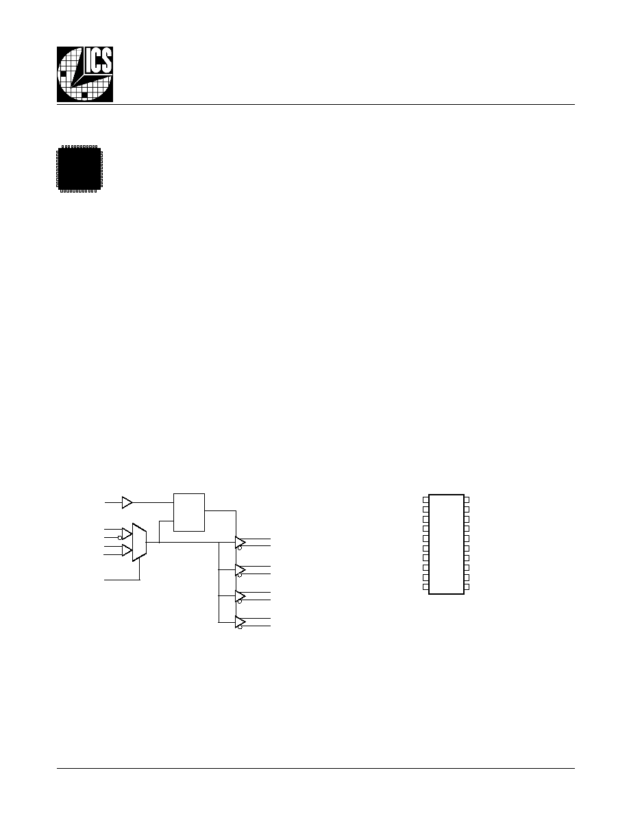
B
LOCK
D
IAGRAM
P
IN
A
SSIGNMENT
ICS8533-11
20-Lead TSSOP
6.5mm x 4.4mm x 0.92 Package Body
G Package
Top View
V
EE
CLK_EN
CLK_SEL
CLK
nCLK
XTAL1
XTAL2
nc
nc
V
CC
1
2
3
4
5
6
7
8
9
10
20
19
18
17
16
15
14
13
12
11
Q0
nQ0
V
CC
Q1
nQ1
Q2
nQ2
V
CC
Q3
nQ3
HiPerClockSTM
,&6
CLK
nCLK
XTAL1
XTAL2
Q0
nQ0
Q1
nQ1
Q2
nQ2
Q3
nQ3
0
1
CLK_EN
CLK_SEL
D
Q
LE
REV. D JULY 16, 2001
2
Integrated
Circuit
Systems, Inc.
ICS8533-11
L
OW
S
KEW
, 1-
TO
-4, C
RYSTAL
O
SCILLATOR
/
D
IFFERENTIAL
-
TO
-3.3V LVPECL F
ANOUT
B
UFFER
T
ABLE
1. P
IN
D
ESCRIPTIONS
T
ABLE
2. P
IN
C
HARACTERISTICS
r
e
b
m
u
N
e
m
a
N
e
p
y
T
n
o
i
t
p
i
r
c
s
e
D
1
V
E
E
r
e
w
o
P
.
d
n
u
o
r
g
o
t
t
c
e
n
n
o
C
.
n
i
p
y
l
p
p
u
s
e
v
i
t
a
g
e
N
2
N
E
_
K
L
C
t
u
p
n
I
p
u
ll
u
P
k
c
o
l
c
s
w
o
ll
o
f
s
t
u
p
t
u
o
k
c
o
l
c
,
H
G
I
H
n
e
h
W
.
e
l
b
a
n
e
k
c
o
l
c
g
n
i
n
o
r
h
c
n
y
S
d
e
c
r
o
f
e
r
a
s
t
u
p
t
u
o
Q
n
,
w
o
l
d
e
c
r
o
f
e
r
a
s
t
u
p
t
u
o
Q
,
W
O
L
n
e
h
W
.
t
u
p
n
i
.
s
l
e
v
e
l
e
c
a
f
r
e
t
n
i
L
T
T
V
L
/
S
O
M
C
V
L
.
h
g
i
h
3
L
E
S
_
K
L
C
t
u
p
n
I
n
w
o
d
ll
u
P
.
t
u
p
n
i
K
L
C
n
,
K
L
C
s
t
c
e
l
e
s
,
W
O
L
n
e
h
W
.
t
u
p
n
i
t
c
e
l
e
s
k
c
o
l
C
.
s
l
e
v
e
l
e
c
a
f
r
e
t
n
i
L
T
T
V
L
/
S
O
M
C
V
L
.
t
u
p
n
i
L
A
T
X
s
t
c
e
l
e
s
,
H
G
I
H
n
e
h
W
4
K
L
C
t
u
p
n
I
n
w
o
d
ll
u
P
.
t
u
p
n
i
k
c
o
l
c
l
a
i
t
n
e
r
e
f
f
i
d
g
n
i
t
r
e
v
n
i
-
n
o
N
5
K
L
C
n
t
u
p
n
I
p
u
ll
u
P
.
t
u
p
n
i
k
c
o
l
c
l
a
i
t
n
e
r
e
f
f
i
d
g
n
i
t
r
e
v
n
I
6
1
L
A
T
X
t
u
p
n
I
n
w
o
d
ll
u
P
.
t
u
p
n
i
r
o
t
a
ll
i
c
s
o
l
a
t
s
y
r
C
7
2
L
A
T
X
t
u
p
n
I
p
u
ll
u
P
.
t
u
p
n
i
r
o
t
a
ll
i
c
s
o
l
a
t
s
y
r
C
9
,
8
c
n
d
e
s
u
n
U
.
t
c
e
n
n
o
c
o
N
8
1
,
3
1
,
0
1
V
C
C
r
e
w
o
P
.
V
3
.
3
o
t
t
c
e
n
n
o
C
.
s
n
i
p
y
l
p
p
u
s
e
v
i
t
i
s
o
P
2
1
,
1
1
3
Q
,
3
Q
n
t
u
p
t
u
O
.
s
l
e
v
e
l
e
c
a
f
r
e
t
n
i
L
C
E
P
V
L
.
s
t
u
p
t
u
o
k
c
o
l
c
l
a
i
t
n
e
r
e
f
f
i
D
5
1
,
4
1
2
Q
,
2
Q
n
t
u
p
t
u
O
.
s
l
e
v
e
l
e
c
a
f
r
e
t
n
i
L
C
E
P
V
L
.
s
t
u
p
t
u
o
k
c
o
l
c
l
a
i
t
n
e
r
e
f
f
i
D
7
1
,
6
1
1
Q
,
1
Q
n
t
u
p
t
u
O
.
s
l
e
v
e
l
e
c
a
f
r
e
t
n
i
L
C
E
P
V
L
.
s
t
u
p
t
u
o
k
c
o
l
c
l
a
i
t
n
e
r
e
f
f
i
D
0
2
,
9
1
0
Q
,
0
Q
n
t
u
p
t
u
O
.
s
l
e
v
e
l
e
c
a
f
r
e
t
n
i
L
C
E
P
V
L
.
s
t
u
p
t
u
o
k
c
o
l
c
l
a
i
t
n
e
r
e
f
f
i
D
:
E
T
O
N
p
u
ll
u
P
d
n
a
n
w
o
d
ll
u
P
.
s
e
u
l
a
v
l
a
c
i
p
y
t
r
o
f
,
s
c
i
t
s
i
r
e
t
c
a
r
a
h
c
n
i
P
,
2
e
l
b
a
T
e
e
S
.
s
r
o
t
s
i
s
e
r
t
u
p
n
i
l
a
n
r
e
t
n
i
o
t
s
r
e
f
e
r
l
o
b
m
y
S
r
e
t
e
m
a
r
a
P
s
n
o
i
t
i
d
n
o
C
t
s
e
T
m
u
m
i
n
i
M
l
a
c
i
p
y
T
m
u
m
i
x
a
M
s
t
i
n
U
C
N
I
e
c
n
a
t
i
c
a
p
a
C
t
u
p
n
I
K
L
C
n
,
K
L
C
4
F
p
L
E
S
_
K
L
C
,
N
E
_
K
L
C
4
F
p
R
P
U
L
L
U
P
r
o
t
s
i
s
e
R
p
u
ll
u
P
t
u
p
n
I
1
5
K
R
N
W
O
D
L
L
U
P
r
o
t
s
i
s
e
R
n
w
o
d
ll
u
P
t
u
p
n
I
1
5
K
8533AG-11
www.icst.com/products/hiperclocks.html
REV. D JULY 16, 2001
3
Integrated
Circuit
Systems, Inc.
ICS8533-11
L
OW
S
KEW
, 1-
TO
-4, C
RYSTAL
O
SCILLATOR
/
D
IFFERENTIAL
-
TO
-3.3V LVPECL F
ANOUT
B
UFFER
T
ABLE
3A. C
ONTROL
I
NPUT
F
UNCTION
T
ABLE
T
ABLE
3B. C
LOCK
I
NPUT
F
UNCTION
T
ABLE
s
t
u
p
n
I
s
t
u
p
t
u
O
N
E
_
K
L
C
L
E
S
_
K
L
C
e
c
r
u
o
S
d
e
t
c
e
l
e
S
3
Q
u
r
h
t
0
Q
3
Q
n
u
r
h
t
0
Q
n
0
0
K
L
C
n
,
K
L
C
W
O
L
;
d
e
l
b
a
s
i
D
H
G
I
H
;
d
e
l
b
a
s
i
D
0
1
2
L
A
T
X
,
1
L
A
T
X
W
O
L
;
d
e
l
b
a
s
i
D
H
G
I
H
;
d
e
l
b
a
s
i
D
1
0
K
L
C
n
,
K
L
C
d
e
l
b
a
n
E
d
e
l
b
a
n
E
1
1
2
L
A
T
X
,
1
L
A
T
X
d
e
l
b
a
n
E
d
e
l
b
a
n
E
r
o
k
c
o
l
c
t
u
p
n
i
g
n
il
l
a
f
d
n
a
g
n
i
s
i
r
a
g
n
i
w
o
l
o
f
d
e
l
b
a
n
e
r
o
d
e
l
b
a
s
i
d
e
r
a
s
t
u
p
t
u
o
k
c
o
l
c
e
h
t
,
s
e
h
c
t
i
w
s
N
E
_
K
L
C
r
e
t
f
A
n
i
n
w
o
h
s
s
a
e
g
d
e
r
o
t
a
ll
i
c
s
o
l
a
t
s
y
r
c
1
e
r
u
g
i
F
.
d
e
b
i
r
c
s
e
d
s
a
s
t
u
p
n
i
2
L
A
T
X
,
1
L
A
T
X
d
n
a
K
L
C
n
,
K
L
C
e
h
t
f
o
n
o
i
t
c
n
u
f
a
e
r
a
s
t
u
p
t
u
o
e
h
t
f
o
e
t
a
t
s
e
h
t
,
e
d
o
m
e
v
i
t
c
a
e
h
t
n
I
.
B
3
e
l
b
a
T
n
i
s
t
u
p
n
I
s
t
u
p
t
u
O
e
d
o
M
t
u
p
t
u
O
o
t
t
u
p
n
I
y
t
i
r
a
l
o
P
K
L
C
K
L
C
n
3
Q
u
r
h
t
0
Q
3
Q
n
u
r
h
t
0
Q
n
0
1
W
O
L
H
G
I
H
l
a
i
t
n
e
r
e
f
f
i
D
o
t
l
a
i
t
n
e
r
e
f
f
i
D
g
n
i
t
r
e
v
n
I
n
o
N
1
0
H
G
I
H
W
O
L
l
a
i
t
n
e
r
e
f
f
i
D
o
t
l
a
i
t
n
e
r
e
f
f
i
D
g
n
i
t
r
e
v
n
I
n
o
N
0
1
E
T
O
N
;
d
e
s
a
i
B
W
O
L
H
G
I
H
l
a
i
t
n
e
r
e
f
f
i
D
o
t
d
e
d
n
E
e
l
g
n
i
S
g
n
i
t
r
e
v
n
I
n
o
N
1
1
E
T
O
N
;
d
e
s
a
i
B
H
G
I
H
W
O
L
l
a
i
t
n
e
r
e
f
f
i
D
o
t
d
e
d
n
E
e
l
g
n
i
S
g
n
i
t
r
e
v
n
I
n
o
N
1
E
T
O
N
;
d
e
s
a
i
B
0
H
G
I
H
W
O
L
l
a
i
t
n
e
r
e
f
f
i
D
o
t
d
e
d
n
E
e
l
g
n
i
S
g
n
i
t
r
e
v
n
I
1
E
T
O
N
;
d
e
s
a
i
B
1
W
O
L
H
G
I
H
l
a
i
t
n
e
r
e
f
f
i
D
o
t
d
e
d
n
E
e
l
g
n
i
S
g
n
i
t
r
e
v
n
I
l
a
i
t
n
e
r
e
f
f
i
d
e
h
t
g
n
i
r
i
w
s
e
s
s
u
c
s
i
d
h
c
i
h
w
,
2
1
e
r
u
g
i
F
,
0
1
e
g
a
p
n
o
n
o
i
t
c
e
s
n
o
i
t
a
m
r
o
f
n
I
n
o
i
t
a
c
il
p
p
A
e
h
t
o
t
r
e
f
e
r
e
s
a
e
l
P
:
1
E
T
O
N
.
s
l
e
v
e
l
d
e
d
n
e
e
l
g
n
i
s
t
p
e
c
c
a
o
t
t
u
p
n
i
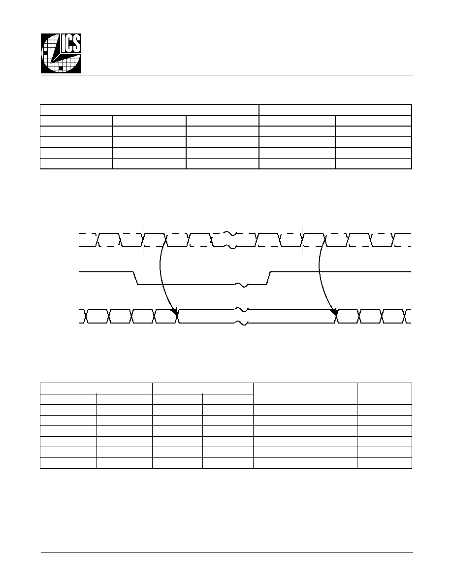
Enabled
Disabled
nCLK
CLK
CLK_EN
nQ0 - nQ3
Q0 - Q3
F
IGURE
1 - CLK_EN T
IMING
D
IAGRAM
REV. D JULY 16, 2001
4
Integrated
Circuit
Systems, Inc.
ICS8533-11
L
OW
S
KEW
, 1-
TO
-4, C
RYSTAL
O
SCILLATOR
/
D
IFFERENTIAL
-
TO
-3.3V LVPECL F
ANOUT
B
UFFER
T
ABLE
4A. P
OWER
S
UPPLY
DC C
HARACTERISTICS
,
V
CC
= 3.3V±5%, T
A
= 0∞C
TO
70∞C
A
BSOLUTE
M
AXIMUM
R
ATINGS
Supply Voltage, V
CCx
4.6V
Inputs, V
I
-0.5V to V
CC
+ 0.5V
Outputs, V
O
-0.5V to V
CC
+ 0.5V
Package Thermal Impedance,
JA
73.2∞C/W (0lfpm)
Storage Temperature, T
STG
-65∞C to 150∞C
Stresses beyond those listed under Absolute Maximum Ratings may cause permanent damage to the device. These
ratings are stress specifications only. Functional operation of product at these conditions or any conditions beyond those
listed in the
DC Characteristics or AC Characteristics is not implied. Exposure to absolute maximum rating conditions for
extended periods may affect product reliability.
T
ABLE
4B. LVCMOS / LVTTL DC C
HARACTERISTICS
,
V
CC
= 3.3V±5%, T
A
= 0∞C
TO
70∞C
T
ABLE
4C. D
IFFERENTIAL
DC C
HARACTERISTICS
,
V
CC
= 3.3V±5%, T
A
= 0∞C
TO
70∞C
l
o
b
m
y
S
r
e
t
e
m
a
r
a
P
s
n
o
i
t
i
d
n
o
C
t
s
e
T
m
u
m
i
n
i
M
l
a
c
i
p
y
T
m
u
m
i
x
a
M
s
t
i
n
U
V
C
C
e
g
a
t
l
o
V
y
l
p
p
u
S
r
e
w
o
P
5
3
1
.
3
3
.
3
5
6
4
.
3
V
I
E
E
t
n
e
r
r
u
C
y
l
p
p
u
S
r
e
w
o
P
0
5
A
m
l
o
b
m
y
S
r
e
t
e
m
a
r
a
P
s
n
o
i
t
i
d
n
o
C
t
s
e
T
m
u
m
i
n
i
M
l
a
c
i
p
y
T
m
u
m
i
x
a
M
s
t
i
n
U
I
H
I
t
n
e
r
r
u
C
h
g
i
H
t
u
p
n
I
K
L
C
n
V
C
C
V
=
N
I
V
5
6
4
.
3
=
5
A
µ
K
L
C
V
C
C
V
=
N
I
V
5
6
4
.
3
=
0
5
1
A
µ
I
L
I
t
n
e
r
r
u
C
w
o
L
t
u
p
n
I
K
L
C
n
V
C
C
V
,
V
5
6
4
.
3
=
N
I
V
0
=
0
5
1
-
A
µ
K
L
C
V
C
C
V
,
V
5
6
4
.
3
=
N
I
V
0
=
5
-
A
µ
V
P
P
e
g
a
t
l
o
V
t
u
p
n
I
k
a
e
P
-
o
t
-
k
a
e
P
5
1
.
0
3
.
1
V
V
R
M
C
;
e
g
a
t
l
o
V
t
u
p
n
I
e
d
o
M
n
o
m
m
o
C
2
,
1
E
T
O
N
V
E
E
5
.
0
+
V
C
C
5
8
.
0
-
V
V
s
i
K
L
C
n
d
n
a
K
L
C
r
o
f
e
g
a
t
l
o
v
t
u
p
n
i
m
u
m
i
x
a
m
e
h
t
s
n
o
i
t
a
c
il
p
p
a
d
e
d
n
e
e
l
g
n
i
s
r
o
F
:
1
E
T
O
N
C
C
.
V
3
.
0
+
V
s
a
d
e
n
i
f
e
d
s
i
e
g
a
t
l
o
v
e
d
o
m
n
o
m
m
o
C
:
2
E
T
O
N
H
I
.
l
o
b
m
y
S
r
e
t
e
m
a
r
a
P
s
n
o
i
t
i
d
n
o
C
t
s
e
T
m
u
m
i
n
i
M
l
a
c
i
p
y
T
m
u
m
i
x
a
M
s
t
i
n
U
V
H
I
e
g
a
t
l
o
V
h
g
i
H
t
u
p
n
I
,
N
E
_
K
L
C
L
E
S
_
K
L
C
2
5
6
7
.
3
V
V
L
I
e
g
a
t
l
o
V
w
o
L
t
u
p
n
I
,
N
E
_
K
L
C
L
E
S
_
K
L
C
3
.
0
-
8
.
0
V
I
H
I
t
n
e
r
r
u
C
h
g
i
H
t
u
p
n
I
N
E
_
K
L
C
V
N
I
V
=
C
C
V
5
6
4
.
3
=
5
A
µ
L
E
S
_
K
L
C
V
N
I
V
=
C
C
V
5
6
4
.
3
=
0
5
1
A
µ
I
L
I
t
n
e
r
r
u
C
w
o
L
t
u
p
n
I
N
E
_
K
L
C
V
N
I
V
,
V
0
=
C
C
V
5
6
4
.
3
=
0
5
1
-
A
µ
L
E
S
_
K
L
C
V
N
I
V
,
V
0
=
C
C
V
5
6
4
.
3
=
5
-
A
µ
8533AG-11
www.icst.com/products/hiperclocks.html
REV. D JULY 16, 2001
5
Integrated
Circuit
Systems, Inc.
ICS8533-11
L
OW
S
KEW
, 1-
TO
-4, C
RYSTAL
O
SCILLATOR
/
D
IFFERENTIAL
-
TO
-3.3V LVPECL F
ANOUT
B
UFFER
T
ABLE
4D. LVPECL DC C
HARACTERISTICS
,
V
CC
= 3.3V±5%, T
A
= 0∞C
TO
70∞C
l
o
b
m
y
S
r
e
t
e
m
a
r
a
P
s
n
o
i
t
i
d
n
o
C
t
s
e
T
m
u
m
i
n
i
M
l
a
c
i
p
y
T
m
u
m
i
x
a
M
s
t
i
n
U
V
H
O
1
E
T
O
N
;
e
g
a
t
l
o
V
h
g
i
H
t
u
p
t
u
O
V
C
C
-
4
.
1
V
C
C
0
.
1
-
V
V
L
O
1
E
T
O
N
;
e
g
a
t
l
o
V
w
o
L
t
u
p
t
u
O
V
C
C
0
.
2
-
V
C
C
7
.
1
-
V
V
G
N
I
W
S
g
n
i
w
S
e
g
a
t
l
o
V
t
u
p
t
u
O
k
a
e
P
-
o
t
-
k
a
e
P
6
.
0
5
8
.
0
V
0
5
h
t
i
w
d
e
t
a
n
i
m
r
e
t
s
t
u
p
t
u
O
:
1
E
T
O
N
V
o
t
C
C
.
V
2
-
T
ABLE
5. C
RYSTAL
C
HARACTERISTICS
r
e
t
e
m
a
r
a
P
s
n
o
i
t
i
d
n
o
C
t
s
e
T
m
u
m
i
n
i
M
l
a
c
i
p
y
T
m
u
m
i
x
a
M
s
t
i
n
U
n
o
i
t
a
ll
i
c
s
O
f
o
e
d
o
M
l
a
t
n
e
m
a
d
n
u
F
e
c
n
a
r
e
l
o
T
y
c
n
e
u
q
e
r
F
0
5
-
0
5
m
p
p
y
t
il
i
b
a
t
S
y
c
n
e
u
q
e
r
F
0
0
1
-
0
0
1
m
p
p
l
e
v
e
L
e
v
i
r
D
1
.
0
W
m
)
R
S
E
(
e
c
n
a
t
s
i
s
e
R
s
e
i
r
e
S
t
n
e
l
a
v
i
u
q
E
0
5
0
8
e
c
n
a
t
i
c
a
p
a
C
t
n
u
h
S
7
F
p
e
c
n
a
t
c
u
d
n
I
n
i
P
s
e
i
r
e
S
3
7
H
n
e
g
n
a
R
e
r
u
t
a
r
e
p
m
e
T
g
n
i
t
a
r
e
p
O
0
0
7
C
∞
g
n
i
g
A
C
∞
5
2
@
r
a
e
y
r
e
P
5
-
5
m
p
p
e
g
n
a
R
y
c
n
e
u
q
e
r
F
4
1
5
2
z
H
M
T
ABLE
6. AC C
HARACTERISTICS
,
V
CC
= 3.3V±5%, T
A
= 0∞C
TO
70∞C
l
o
b
m
y
S
r
e
t
e
m
a
r
a
P
s
n
o
i
t
i
d
n
o
C
t
s
e
T
m
u
m
i
n
i
M
l
a
c
i
p
y
T
m
u
m
i
x
a
M
s
t
i
n
U
f
X
A
M
y
c
n
e
u
q
e
r
F
t
u
p
n
I
m
u
m
i
x
a
M
0
5
6
z
H
M
t
D
P
1
E
T
O
N
;
y
a
l
e
D
n
o
i
t
a
g
a
p
o
r
P
z
H
M
0
5
6
0
.
1
0
.
2
s
n
t
)
o
(
k
s
5
,
2
E
T
O
N
;
w
e
k
S
t
u
p
t
u
O
0
3
s
p
t
)
p
p
(
k
s
5
,
3
E
T
O
N
;
w
e
k
S
t
r
a
P
-
o
t
-
t
r
a
P
0
5
1
s
p
t
R
e
m
i
T
e
s
i
R
t
u
p
t
u
O
z
H
M
0
5
@
%
0
8
o
t
%
0
2
0
0
3
0
0
7
s
p
t
F
e
m
i
T
ll
a
F
t
u
p
t
u
O
z
z
H
M
0
5
@
%
0
8
o
t
%
0
2
0
0
3
0
0
7
s
p
c
d
o
4
E
T
O
N
;
e
l
c
y
C
y
t
u
D
t
u
p
t
u
O
7
4
0
5
3
5
%
L
O
T
c
s
o
e
c
n
a
r
e
ll
o
T
r
o
t
a
ll
i
c
s
O
l
a
t
s
y
r
C
D
B
T
m
p
p
.
e
s
i
w
r
e
h
t
o
d
e
t
o
n
s
s
e
l
n
u
z
H
M
0
0
5
t
a
d
e
r
u
s
a
e
m
s
r
e
t
e
m
a
r
a
p
ll
A
.
r
e
t
t
ij
d
d
a
t
o
n
s
e
o
d
t
r
a
p
e
h
T
.
t
u
p
t
u
o
e
h
t
n
o
r
e
t
t
ij
e
h
t
l
a
u
q
e
ll
i
w
t
u
p
n
i
e
h
t
n
o
r
e
t
t
ij
e
l
c
y
c
-
o
t
-
e
l
c
y
c
e
h
T
.
t
n
i
o
p
g
n
i
s
s
o
r
c
t
u
p
t
u
o
l
a
i
t
n
e
r
e
f
f
i
d
e
h
t
o
t
t
n
i
o
p
g
n
i
s
s
o
r
c
t
u
p
n
i
l
a
i
t
n
e
r
e
f
f
i
d
e
h
t
m
o
r
f
d
e
r
u
s
a
e
M
:
1
E
T
O
N
.
s
n
o
i
t
i
d
n
o
c
d
a
o
l
l
a
u
q
e
h
t
i
w
d
n
a
e
g
a
t
l
o
v
y
l
p
p
u
s
e
m
a
s
e
h
t
t
a
s
t
u
p
t
u
o
n
e
e
w
t
e
b
w
e
k
s
s
a
d
e
n
i
f
e
D
:
2
E
T
O
N
.
s
t
n
i
o
p
s
s
o
r
c
l
a
i
t
n
e
r
e
f
f
i
d
t
u
p
t
u
o
e
h
t
t
a
d
e
r
u
s
a
e
M
s
e
g
a
t
l
o
v
y
l
p
p
u
s
e
m
a
s
e
h
t
t
a
g
n
i
t
a
r
e
p
o
s
e
c
i
v
e
d
t
n
e
r
e
f
f
i
d
n
o
s
t
u
p
t
u
o
n
e
e
w
t
e
b
w
e
k
s
s
a
d
e
n
i
f
e
D
:
3
E
T
O
N
d
e
r
u
s
a
e
m
e
r
a
s
t
u
p
t
u
o
e
h
t
,
e
c
i
v
e
d
h
c
a
e
n
o
s
t
u
p
n
i
f
o
e
p
y
t
e
m
a
s
e
h
t
g
n
i
s
U
.
s
n
o
i
t
i
d
n
o
c
d
a
o
l
l
a
u
q
e
h
t
i
w
d
n
a
.
s
t
n
i
o
p
s
s
o
r
c
l
a
i
t
n
e
r
e
f
f
i
d
e
h
t
t
a
.
e
t
o
N
n
o
i
t
a
c
il
p
p
A
o
t
r
e
f
e
r
,
t
u
p
n
i
L
A
T
X
r
o
F
.
K
L
C
g
n
i
s
u
d
e
r
u
s
a
e
M
:
4
E
T
O
N
.
5
6
d
r
a
d
n
a
t
S
C
E
D
E
J
h
t
i
w
e
c
n
a
d
r
o
c
c
a
n
i
d
e
n
i
f
e
d
s
i
r
e
t
e
m
a
r
a
p
s
i
h
T
:
5
E
T
O
N
REV. D JULY 16, 2001
6
Integrated
Circuit
Systems, Inc.
ICS8533-11
L
OW
S
KEW
, 1-
TO
-4, C
RYSTAL
O
SCILLATOR
/
D
IFFERENTIAL
-
TO
-3.3V LVPECL F
ANOUT
B
UFFER
P
ARAMETER
M
EASUREMENT
I
NFORMATION
F
IGURE
3 - D
IFFERENTIAL
I
NPUT
L
EVEL
CLK
nCLK
V
CC
V
EE
V
CMR
Cross Points
V
PP
F
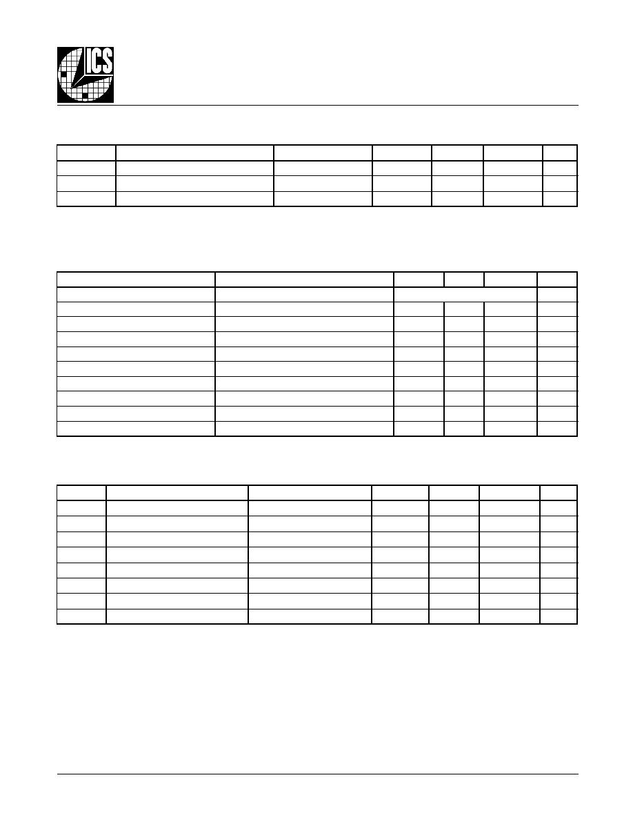
IGURE
2 - O
UTPUT
L
OAD
T
EST
C
IRCUIT
SCOPE
Qx
nQx
LVPECL
V
CC
V
CC
=
2V
V
EE
=
-1.3V ± 0.135V
8533AG-11
www.icst.com/products/hiperclocks.html
REV. D JULY 16, 2001
7
Integrated
Circuit
Systems, Inc.
ICS8533-11
L
OW
S
KEW
, 1-
TO
-4, C
RYSTAL
O
SCILLATOR
/
D
IFFERENTIAL
-
TO
-3.3V LVPECL F
ANOUT
B
UFFER
F
IGURE
7 - odc & t
PERIOD
Pulse Width
t
PERIOD
t
PW
t
PERIOD
odc =
CLK, Q0 - Q3
nCLK, nQ0 - nQ3
F
IGURE
6 - P
ROPAGATION
D
ELAY
t
PD
CLK
nCLK
Q0 - Q3
nQ0 - nQ3
Clock Inputs
and Outputs
20%
80%
20%
80%
t
R
t
F
V
S W I N G
F
IGURE
5 - I
NPUT
AND
O
UTPUT
R
ISING
/F
ALL
T
IME
F
IGURE
4 - O
UTPUT
S
KEW
tsk(o)
Qx
nQx
Qy
nQy
REV. D JULY 16, 2001
8
Integrated
Circuit
Systems, Inc.
ICS8533-11
L
OW
S
KEW
, 1-
TO
-4, C
RYSTAL
O
SCILLATOR
/
D
IFFERENTIAL
-
TO
-3.3V LVPECL F
ANOUT
B
UFFER
A
PPLICATION
I
INFORMATION
C
RYSTAL
O
SCILLATOR
C
IRCUIT
F
REQUENCY
F
INE
T
UNING
A crystal can be characterized for either series or parallel mode operation. The ICS8533-11 and ICS8535-11 fanout buffers have
built-in crystal oscillator circuits that can accept either a series or parallel crystal without additional components. The frequency
accuracy provided by this configuration is sufficient for most computer applications.
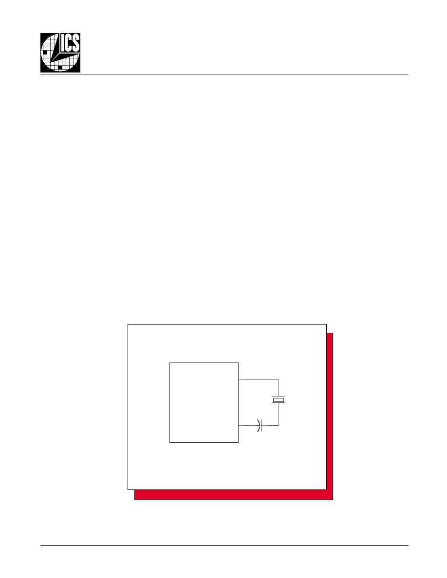
For applications requiring highly accurate clock frequencies, the output frequency can be fine tuned by inserting a small series
capacitor C1 at the XTAL1 input (Pin 6 for ICS8533-11) as shown in
Figure 8. This fine tuning approach can be applied in either
parallel or series crystal. The C1 value depends on the crystal type, frequency and the board layout. The parallel crystal fine
tuning results in smaller ppm and better performance. It is difficult to provide the precise value of C1. This section provides
recommended series capacitor C1 values to start with. This example uses 18pF parallel crystals.
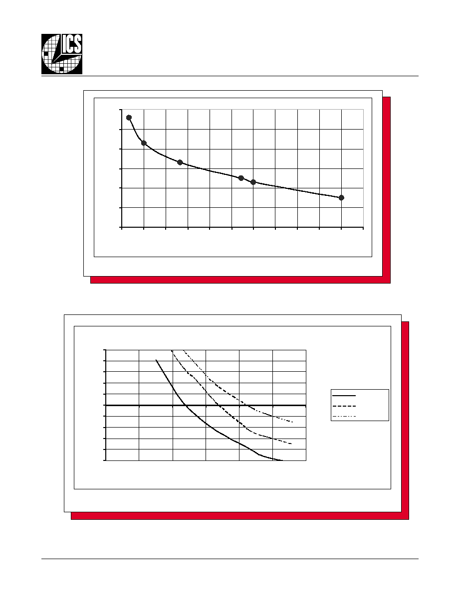
Figure 9shows the suggested series capacitor value for a parallel crystal. For a 16.666 MHz crystal, the recommended C1 value is
about 33pF.
Figure 10 shows frequency accuracy versus series capacitance for 19.44MHz, 16.666MHz and 15MHz crystals. As seen from this
figure, a 24pF, 33pF and 43pF series capacitor is used to achieve the lowest ppm error for 19.44MHz, 16.666MHz and 15MHz
respectively.
Figure 11 shows the experiment results of crystal oscillator frequency drift due to temperature variation.
X1
U1
XTAL2
XTAL1
C1
F
IGURE
8 - C
RYSTAL
I
NTERFACE
WITH
S
ERIES
C
APACITOR
C1
.
8533AG-11
www.icst.com/products/hiperclocks.html
REV. D JULY 16, 2001
9
Integrated
Circuit
Systems, Inc.
ICS8533-11
L
OW
S
KEW
, 1-
TO
-4, C
RYSTAL
O
SCILLATOR
/
D
IFFERENTIAL
-
TO
-3.3V LVPECL F
ANOUT
B
UFFER
14.318
15.000
16.666
19.440
20.000
24.000
0
10
20
30
40
50
60
14
15
16
17
18
19
20
21
22
23
24
25
Crystal Frequency (MHz)
Ser
i
es C
a
paci
t
o
r
,
C
1
(
p
F
)
F
IGURE
9 - S
UGGESTED
S
ERIES
C
APACITOR
C1
FOR
P
ARALLEL
C
RYSTAL
-100
-80
-60
-40
-20
0
20
40
60
80
100
0
10
20
30
40
50
60
Series Capacitor, C1 (pF)
Fr
equenc
y
A
ccur
a
c
y
(
ppm
)
19.44MHz
16.666MHz
15.00MHz
F
IGURE
10 - F
REQUENCY
A
CCURACY
FOR
P
ARALLEL
C
RYSTAL
U
SING
S
ERIES
C
APACITOR
C1
REV. D JULY 16, 2001
10
Integrated
Circuit
Systems, Inc.
ICS8533-11
L
OW
S
KEW
, 1-
TO
-4, C
RYSTAL
O
SCILLATOR
/
D
IFFERENTIAL
-
TO
-3.3V LVPECL F
ANOUT
B
UFFER
-60
-40
-20
0
20
40
60
0
10
20
30
40
50
60
70
80
Temperature (deg. C)
Fr
equec
y
Dr
i
f
t
e
d (
ppm
)
19.44MHz
16.666MHz
F
IGURE
11 - C
RYSTAL
O
SCILLATOR
C
RCUIT
F
REQUENCY
D
RIFTED
D
UE
TO
T
EMPERATURE
V
ARIATION
W
IRING
THE
D
IFFERENTIAL
I
NPUT
TO
A
CCEPT
S
INGLE
E
NDED
L
EVELS
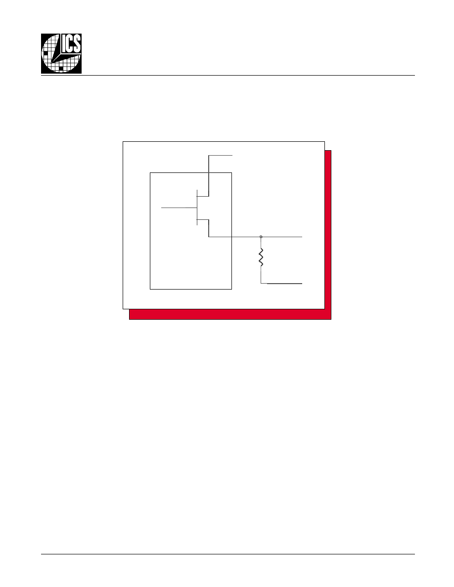
Figure 12 shows how the differential input can be wired to accept single ended levels. The reference voltage V_REF ~ V
CC
/2 is
generated by the bias resistors R1, R2 and C1. This bias circuit should be located as close as possible to the input pin. The ratio of
R1 and R2 might need to be adjusted to position the V_REF in the center of the input voltage swing. For example, if the input clock
swing is only 2.5V and V
CC
= 3.3V, V_REF should be 1.25V and R2/R1 = 0.609.
F
IGURE
12: S
INGLE
E
NDED
S
IGNAL
D
RIVING
D
IFFERENTIAL
I
NPUT
R2
1K
V
CC
CLK_IN
+
-
R1
1K
C1
0.1uF
V_REF

8533AG-11
www.icst.com/products/hiperclocks.html
REV. D JULY 16, 2001
11
Integrated
Circuit
Systems, Inc.
ICS8533-11
L
OW
S
KEW
, 1-
TO
-4, C
RYSTAL
O
SCILLATOR
/
D
IFFERENTIAL
-
TO
-3.3V LVPECL F
ANOUT
B
UFFER
P
OWER
C
ONSIDERATIONS
This section provides information on power dissipation and junction temperature for the ICS8533-11.
Equations and example calculations are also provided.
1. Power Dissipation.
The total power dissipation for the ICS8533-11 is the sum of the core power plus the power dissipated in the load(s).
The following is the power dissipation for V
CC
= 3.3V + 5% = 3.465V, which gives worst case results.
NOTE: Please refer to Section 3 for details on calculating power dissipated in the load.
∑
Power (core)
MAX
= V
CC_MAX
* I
EE_MAX
= 3.465V * 50mA = 173.3mW
∑
Power (outputs)
MAX
= 30.2mW/Loaded Output pair
If all outputs are loaded, the total power is 4 * 30.2mW = 120.8mW
Total Power
_MAX
(3.465V, with all outputs switching) = 173.3mW + 120.8mW = 294.1mW
2. Junction Temperature.
Junction temperature, Tj, is the temperature at the junction of the bond wire and bond pad and directly affects the reliability of the
device. The maximum recommended junction temperature for HiPerClockS
TM
devices is 125∞C.
The equation for Tj is as follows: Tj =
JA
* Pd_total + T
A
Tj = Junction Temperature
JA
= junction-to-ambient thermal resistance
Pd_total = Total device power dissipation (example calculation is in section 1 above)
T
A
= Ambient Temperature
In order to calculate junction temperature, the appropriate junction-to-ambient thermal resistance
JA
must be used
. Assuming a
moderate air flow of 200 linear feet per minute and a multi-layer board, the appropriate value is 66.6∞C/W per Table 6 below.
Therefore, Tj for an ambient temperature of 70∞C with all outputs switching is:
70∞C + 0.294W * 66.6∞C/W = 89.58∞C. This is well below the limit of 125∞C
This calculation is only an example. Tj will obviously vary depending on the number of loaded outputs, supply voltage, air flow,
and the type of board (single layer or multi-layer).
q
JA
by Velocity (Linear Feet per Minute)
0
200
500
Single-Layer PCB, JEDEC Standard Test Boards 114.5∞C/W
98.0∞C/W
88.0∞C/W
Multi-Layer PCB, JEDEC Standard Test Boards
73.2∞C/W
66.6∞C/W
63.5∞C/W
NOTE: Most modern PCB designs use multi-layered boards. The data in the second row pertains to most designs.
Table 7. Thermal Resistance
q
JA
for 20-pin TSSOP, Forced Convection
REV. D JULY 16, 2001
12
Integrated
Circuit
Systems, Inc.
ICS8533-11
L
OW
S
KEW
, 1-
TO
-4, C
RYSTAL
O
SCILLATOR
/
D
IFFERENTIAL
-
TO
-3.3V LVPECL F
ANOUT
B
UFFER
3. Calculations and Equations.
The purpose of this section is to derive the power dissipated into the load.
LVPECL output driver circuit and termination are shown in
Figure 8.
T
o calculate worst case power dissipation into the load, use the following equations which assume a 50
load, and a termination
voltage of V
CC
- 2V.
Pd_H is power dissipation when the output drives high.
Pd_L is the power dissipation when the output drives low.
Pd_H = [(V
OH_MAX
≠ (V
CC_MAX
- 2V))/R
L
] * (V
CC_MAX
- V
OH_MAX
)
Pd_L = [(V
OL_MAX
≠ (V
CC_MAX
- 2V))/R
L
] * (V
CC_MAX
- V
OL_MAX
)
∑
For logic high, V
OUT
= V
OH_MAX
= V
CC_MAX
≠ 1.0V
Using V
CC_MAX
= 3.465, this results in V
OH_MAX
= 2.465V
∑
For logic low, V
OUT
= V
OL_MAX
= V
CC_MAX
≠ 1.7V
Using V
CC_MAX
= 3.465, this results in V
OL_MAX
= 1.765V
Pd_H = [(2.465V - (3.465V - 2V))/50
] * (3.465V - 2.465V) = 20mW
Pd_L = [(1.765V - (3.465V - 2V))/50
] * (3.465V - 1.765V) = 10.2mW
Total Power Dissipation per output pair = Pd_H + Pd_L = 30.2mW
F
IGURE
13 - LVPECL D
RIVER
C
IRCUIT
AND
T
ERMINATION
Q1
V
OUT
V
CC
RL
50
V
CC
- 2V

8533AG-11
www.icst.com/products/hiperclocks.html
REV. D JULY 16, 2001
13
Integrated
Circuit
Systems, Inc.
ICS8533-11
L
OW
S
KEW
, 1-
TO
-4, C
RYSTAL
O
SCILLATOR
/
D
IFFERENTIAL
-
TO
-3.3V LVPECL F
ANOUT
B
UFFER
R
ELIABILITY
I
NFORMATION
T
RANSISTOR
C
OUNT
The transistor count for ICS8533-11 is: 428
T
ABLE
8.
JA
VS
. A
IR
F
LOW
T
ABLE
q
JA
by Velocity (Linear Feet per Minute)
0
200
500
Single-Layer PCB, JEDEC Standard Test Boards 114.5∞C/W
98.0∞C/W
88.0∞C/W
Multi-Layer PCB, JEDEC Standard Test Boards
73.2∞C/W
66.6∞C/W
63.5∞C/W
NOTE: Most modern PCB designs use multi-layered boards. The data in the second row pertains to most designs.
REV. D JULY 16, 2001
14
Integrated
Circuit
Systems, Inc.
ICS8533-11
L
OW
S
KEW
, 1-
TO
-4, C
RYSTAL
O
SCILLATOR
/
D
IFFERENTIAL
-
TO
-3.3V LVPECL F
ANOUT
B
UFFER
P
ACKAGE
O
UTLINE
- G S
UFFIX
T
ABLE
9. P
ACKAGE
D
IMENSIONS
Reference Document: JEDEC Publication 95, MS-153
L
O
B
M
Y
S
s
r
e
t
e
m
i
l
l
i
M
N
I
M
X
A
M
N
0
2
A
-
-
0
2
.
1
1
A
5
0
.
0
5
1
.
0
2
A
0
8
.
0
5
0
.
1
b
9
1
.
0
0
3
.
0
c
9
0
.
0
0
2
.
0
D
0
4
.
6
0
6
.
6
E
C
I
S
A
B
0
4
.
6
1
E
0
3
.
4
0
5
.
4
e
C
I
S
A
B
5
6
.
0
L
5
4
.
0
5
7
.
0
∞
0
∞
8
a
a
a
-
-
0
1
.
0
8533AG-11
www.icst.com/products/hiperclocks.html
REV. D JULY 16, 2001
15
Integrated
Circuit
Systems, Inc.
ICS8533-11
L
OW
S
KEW
, 1-
TO
-4, C
RYSTAL
O
SCILLATOR
/
D
IFFERENTIAL
-
TO
-3.3V LVPECL F
ANOUT
B
UFFER
T
ABLE
10. O
RDERING
I
NFORMATION
While the information presented herein has been checked for both accuracy and reliability, Integrated Circuit Systems, Incorporated (ICS) assumes no responsibility for either its use or
for infringement of any patents or other rights of third parties, which would result from its use. No other circuits, patents, or licenses are implied. This product is intended for use in normal
commercial applications. Any other applications such as those requiring extended temperature range, high reliability, or other extraordinary environmental requirements are not recom-
mended without additional processing by ICS. ICS reserves the right to change any circuitry or specifications without notice. ICS does not authorize or warrant any ICS product for use in
life support devices or critical medical instruments.
r
e
b
m
u
N
r
e
d
r
O
/
t
r
a
P
g
n
i
k
r
a
M
e
g
a
k
c
a
P
t
n
u
o
C
e
r
u
t
a
r
e
p
m
e
T
1
1
-
G
A
3
3
5
8
S
C
I
1
1
-
G
A
3
3
5
8
S
C
I
P
O
S
S
T
d
a
e
l
0
2
e
b
u
t
r
e
p
2
7
C
∞
0
7
o
t
C
∞
0
T
1
1
-
G
A
3
3
5
8
S
C
I
1
1
-
G
A
3
3
5
8
S
C
I
l
e
e
R
d
n
a
e
p
a
T
n
o
P
O
S
S
T
d
a
e
l
0
2
0
0
5
2
C
∞
0
7
o
t
C
∞
0