87972DYI
www.icst.com/products/hiperclocks.html
REV. A OCTOBER 18, 2002
1
Integrated
Circuit
Systems, Inc.
ICS87972I
L
OW
S
KEW
, 1-
TO
-12
LVCMOS C
LOCK
M
ULTIPLIER
/Z
ERO
D
ELAY
B
UFFER
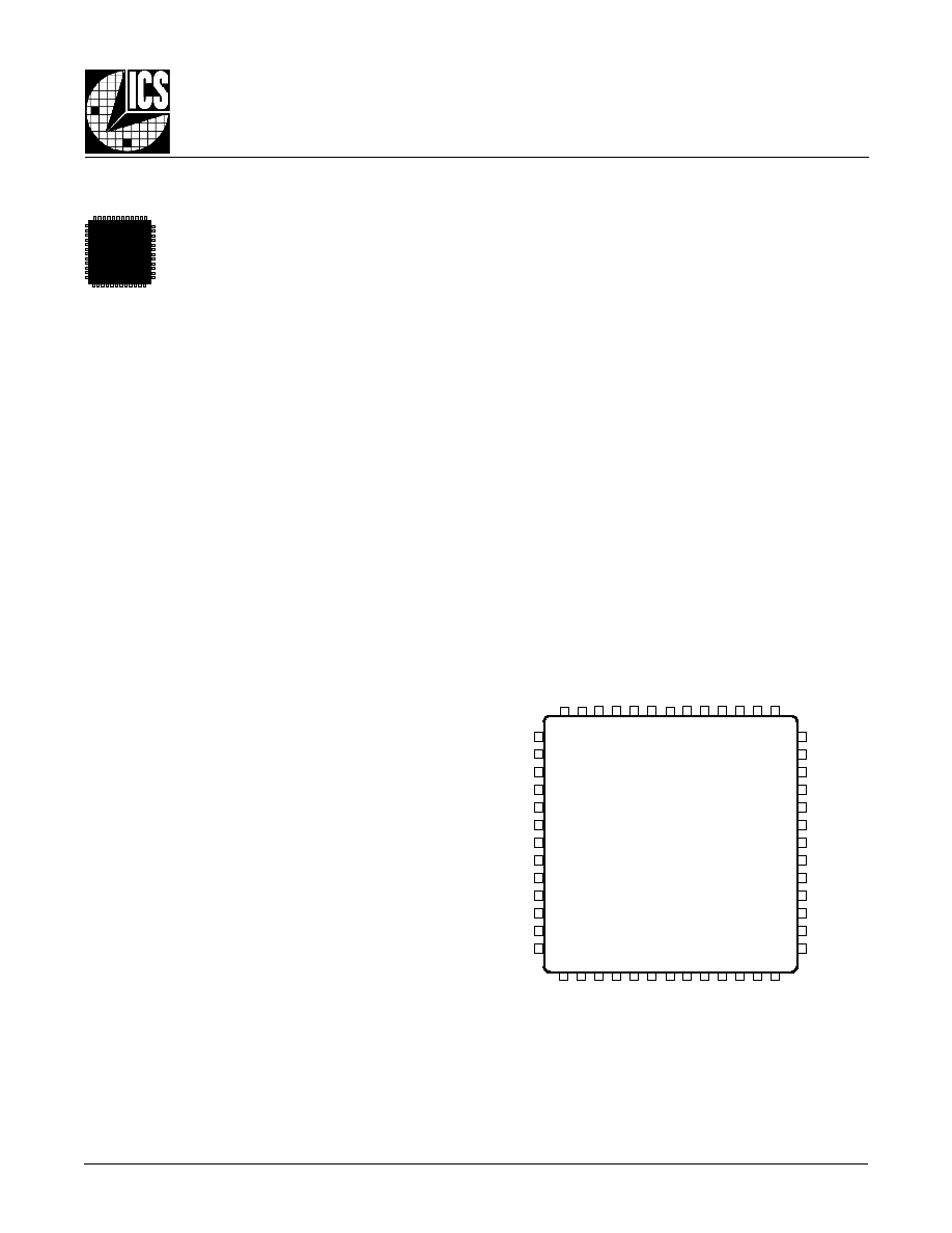
P
IN
A
SSIGNMENT
G
ENERAL
D
ESCRIPTION
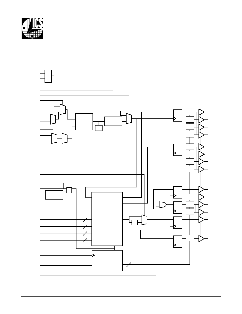
The ICS87972I is a LVCMOS clock generator
and a member of the HiPerClockSTM family of High
Performance Clock Solutions from ICS. The
ICS87972I has three selectable inputs and pro-
vides 14 LVCMOS outputs.
The ICS87972I is a highly flexible device. Using the crystal os-
cillator input, it can be used to generate clocks for a system. All
of these clocks can be the same frequency or the device can be
configured to generate up to three different frequencies among
the three output banks. Using one of the single ended inputs, the
ICS87972I can be used as a zero delay buffer/multiplier/divider
in clock distribution applications.
The three output banks and feedback output each have their
own output dividers which allows the device to generate a
multitude of different bank frequency ratios and output-to-input
frequency ratios. In addition, 2 outputs in Bank C (QC2, QC3)
can be selected to be inverting or non-inverting. The output
frequency range is 8.33MHz - 125MHz.
Input frequency range is
5MHz - 120MHz.
The ICS87972I also has a QSYNC output which can be used
for system synchronization purposes. It monitors Bank A and
Bank C outputs and goes low one period of the faster clock prior
to coincident rising edges of Bank A and Bank C clocks. QSYNC
then goes high again when the coincident rising edges of Bank A
and Bank C occur. This feature is used primarily in applications
where Bank A and Bank C are running at different frequencies,
and is particularly useful when they are running at non-integer
multiples of one another.
Example Applications:
1.
System Clock generator: Use a 16.66 MHz Crystal to
generate eight 33.33MHz copies for PCI and four 100MHz
copies for the CPU or PCI-X.
2.
Line Card Multiplier: Multiply 19.44MHz from a back plane
to 77.76MHz for the line Card ASICs and Serdes.
3.
Zero Delay buffer for Synchronous memory: Fan out up
to twelve 100MHz copies from a memory controller ref-
erence clock to the memory chips on a memory module
with zero delay.
F
EATURES
·
Fully integrated PLL
·
14 LVCMOS outputs; (12) clocks, (1) feedback, (1) sync
·
Selectable crystal oscillator interface or LVCMOS reference
clock inputs
·
CLK0, CLK1 can accept the following input levels:
LVCMOS or LVTTL
·
Output frequency range: 8.33MHz to 125MHz
·
VCO range: 200MHz to 480MHz
·
Output skew: 550ps (maximum)
·
Cycle-to-cycle jitter: ±100ps (typical)
·
Full 3.3V supply voltage
·
-40°C to 85°C ambient operating temperature
·
Pin compatible with MPC972
·
Compatible with PowerPCTM and PentiumTM Microprocessors
FSEL_FB0
V
DD
QFB
GNDO
EXT_FB
QB3
V
DDO
QB2
GNDO
QB1
V
DDO
QB0
GNDO
40
41
42
43
44
45
46
47
48
49
50
51
52
1 2 3 4 5 6 7 8 9 10 11 12 13
26
25
24
23
22
21
20
19
18
17
16
15
14
39 38 37 36 35 34 33 32 31 30 29 28 27
FSEL_B1
FSEL_B0
FSEL_A1
FSEL_A0
QA3
V
DDO
QA2
GNDO
QA1
V
DDO
QA0
GNDO
VCO_SEL
FSEL_FB1
QSYNC
GNDO
QC0
V
DDO
QC1
FSEL_C0
FSEL_C1
QC2
V
DDO
QC3
GNDO
INV_CLK
V
DDA
XT
AL2
XT
AL1
CLK1
CLK0
CLK_SEL
REF_SEL
PLL_SEL
FSEL_FB2
FRZ_DA
T
A
FRZ_CLK
nMR/OE
GNDI
52-Lead LQFP
10mm x 10mm x 1.4mm package body
Y package
Top View
ICS87972I
HiPerClockSTM
,&6