/home/web/doc/html/icst/213872
Integrated
Circuit
Systems, Inc.
General Description
Features
ICS9178-03
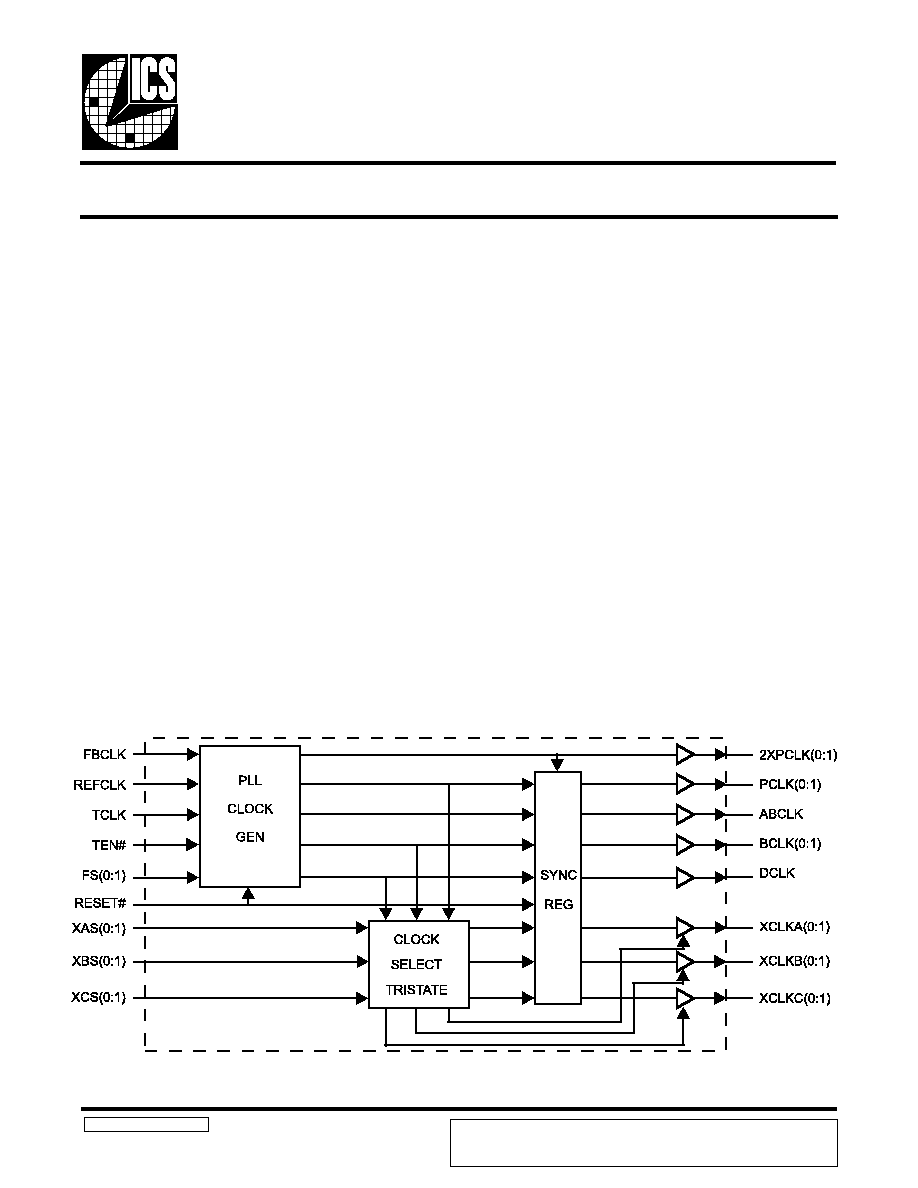
Block Diagram
ICS9178-03 Rev C 02/12/98P
245 MHz Clock Generator and Integrated Buffer for PowerPC
The ICS9178-03 generates all clocks required for high speed
PowerPC RISC microprocessor systems. Generating clocks
in phase with an external reference frequency allows the
ICS9178-03 to be used as a multiplying zero delay buffer.
Three different multiplying factors are externally selectable.
These factors can be customized for specific applications. An
external frequency can be directly applied to aid system
testing. With 2X processor clock speeds up to 245 MHz,
PECL outputs are provided. User selectable frequency ratios
are available for PCLK/BCLK and PCLK/XCLK. Each pair of
clocks outputs have separate supply pins to minimize output
jitter and allow them to operate at 5V, 3.3V or custom voltage
levels.
Generates 2 PECL 2x processor, 2 TTL/CMOS 1x
processor and 10 selectable bus clocks
2XPCLK ranges from 75 MHz to 245 MHz (5V or
5V/3.3V mixed supply) or 60 to 170 MHz (3.3V only)
Asymmetric duty cycle bus clock for PowerPC
Bus to processor clock skews less than �250ps
2XPCLK to PCLK skew controlled at 300 �300ps
Selectable reference multiplying factors
Selectable PCLK/BCLK and PCLK/XCLK ratios
Separate supplies allow 5V and 3.3V output mix
3.0V - 5.5V supply range
44-pin PQFP package
PowerPC is a trademark of Motorola Corporation.
Applications
Ideal for high-speed systems based on PowerPC
ICS reserves the right to make changes in the device data identified in this publication
without further notice. ICS advises its customers to obtain the latest version of all
device data to verify that any information being relied upon by the customer is current
and accurate.
2
ICS9178-03
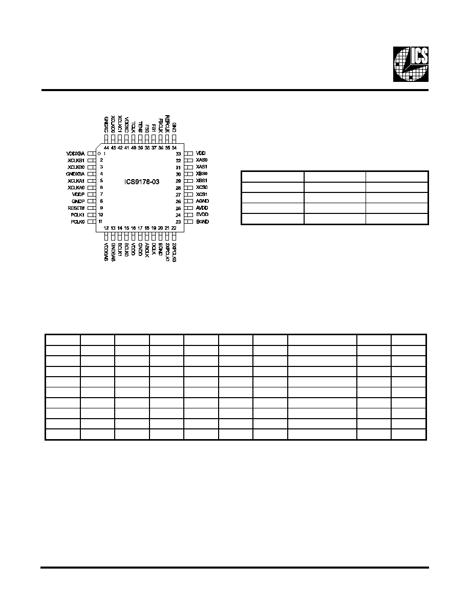
Pin Configuration
44-Pin PQFP
*VCO range is limited from 75- 245 MHz at 5V �5% and 60 - 170 MHz at 3.3V �5%. Divide ratios assume BCLK is externally
fed back to FBCLK.
_=A,B,C
Functionality
The 2XPCLK series or Thevinen trace terminations must be optimized for the specific operating frequency and board
layout. The rising edge of ABCLK is coincident with the rising edges of 2XPCLK, PCLK and other BCLKs.
X_S1
X_S0
XCLK_(0,1)
0
0
PCLK
0
1
BCLK
1
0
DCLK
1
1
Tristate
FS1
FS0
RST
TEN
*VCO
2XPCLK
PCLK
ABCLK (H/L%)
BCLK
DCLK
0
0
1
0
6x REF
VCO
VCO/2
VCO/6 (66/33)
VCO/6
VCO/4
0
1
1
0
8x REF
VCO
VCO/2
VCO/8 (75/25)
VCO/8
VCO/4
1
0
1
0
4x REF
VCO
VCO/2
VCO/12 (50/50)
VCO/4
VCO/4
1
1
1
0
X
1
1
1
1
1
X
X
0
X
X
0
0
0
0
0
0
0
1
1
TCLK
TCLK
TCLK/2
TCLK/6 (66/33)
TCLK/6
TCLK/4
0
1
1
1
TCLK
TCLK
TCLK/2
TCLK/8 (75/25)
TCLK/8
TCLK/4
1
0
1
1
TCLK
TCLK
TCLK/2
TCLK/12 ( 66/33)
TCLK/12
TCLK/4
1
1
1
1
TCLK
TCLK
TCLK/2
TCLK/2
TCLK/2
TCLK/4
3
ICS9178-03
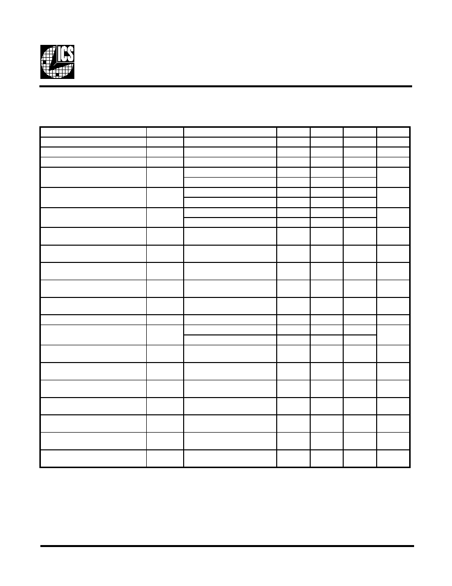
Pin Description
*=Pin is pulled-up to VDD internally by the device.
PIN NUMBER
PIN NAME
TYPE
DESCRIPTION
32
XAS0
Input
LSB Programmable Group A frequency selector.
31
XAS1
Input
MSB Programmable Group A frequency selector.
6
XCLKA0
Output
TTL/CMOS group A programmable clock output.
5
XCLKA1
Output
TTL/CMOS group A programmable clock output.
30
XBS0
Input
LSB Programmable Group B frequency selector.
29
XBS1
Input
MSB Programmable Group B frequency selector.
3
XCLKB0
Output
TTL/CMOS Group B programmable clock output.
2
XCLKB1
Output
TTL/CMOS Group B programmable clock output.
1
VDDXBA
--
Power for programmable Group A and B buffers (Pins 2, 3, 5, 6).
4
GNDXBA
--
Ground for programmable Group A and B buffers (Pins 2, 3, 5, 6).
44
GNDXC
--
Ground for the programmable Group C buffers (Pins 42 and 43).
43
XCLKC0
Output
TTL/CMOS Group C programmable clock output.
42
XCLKC1
Output
TTL/CMOS Group C programmable clock output.
41
VDDXC
--
Power for the XC signal output buffers (Pins 42 and 43).
28
XCS0
Input
LSB Programmable Group C frequency selector.
27
XCS1
Input
MSB Programmable Group C frequency selector.
11
PCLK0
Output
TTL/CMOS 1X Processor clock output.
10
PCLK1
Output
TTL/CMOS 1X Processor clock output.
8
GNDP
--
Ground for PCLK output buffers (Pins 11 and 10).
7
VDDP
--
Power for PCLK output buffers (Pins 11 and 10).
22
2XPCLK0
Output
PECL 2X Processor clock output.
21
2XPCLK1
Output
PECL 2X Processor clock output.
24
EVDD
--
Power for PECL buffers (Pins 21 and 22).
23
EGND
--
Ground for PECL buffers (Pins 21 and 22).
20
EGND
--
Ground for PECL buffers (Pins 21 and 22).
38*
FS0
Input
LSB frequency select PLL (divider mode control).
37*
FS1
Input
MSB frequency select PLL (divider mode control).
36
FBCLK
Input
External PLL feedback path from one of the BCLK outputs.
35
REFCLK
Input
External reference clock input.
25
AVDD
--
Power for the analog PLL circuitry.
26
AGND
--
Ground for the analog PLL circuitry.
19
DCLK
Output
TTL/CMOS D clock output.
16
VDDD
--
Power for D output buffers (Pin 19).
17
GNDD
--
Ground for D output buffer (Pin 19).
15
BCLK0
Output
TTL/CMOS B (Bus) clock output.
14
BCLK1
Output
TTL/CMOS B (Bus) clock output.
13
GNDBAB
--
Ground for output buffers AB and B clocks (Pins 14, 15 & 18).
12
VDDBAB
--
Power for output buffers AB and B clocks (Pins 14, 15 & 18).
18
ABCLK
Output
TTL/CMOS AB Bus clock (has Asymmetric duty cycle).
40
TCLK
Input
External test clock input.
39
TEN#
Input
Test enable (tie low).
9
RESET#
Input
Sync register reset (active low).
33
VDD
--
Digital power supply for 5.0 or 3.3V.
34
GND
--
Digital ground supply.
4
ICS9178-03
Absolute Maximum Ratings
VDD referenced to GND . . . . . . . . . . . . . . . . . . . . . . 7V
Operating temperature under bias. . . . . . . . . . . . . . . . 0�C to +70�C
Storage temperature . . . . . . . . . . . . . . . . . . . . . . . . . . -65�C to +150�C
Voltage on I/O pins referenced to GND. . . . . . . . . . . GND -0.5V to VDD +0.5V
Power dissipation . . . . . . . . . . . . . . . . . . . . . . . . . . . . 0.5 Watts
Stresses above those listed under Absolute Maximum Ratings may cause permanent damage to the device. This is a stress rating
only and functional operation of the device at these or any other conditions above those indicated in the operational sections
of the specifications is not implied. Exposure to absolute maximum rating conditions for extended periods may affect product
reliability.
Electrical Characteristics
Device Specifications
DC Characteristics
VDD =+5V �5%, 0�C
TAMBIENT
+70�C unless otherwise stated
Note 1: Parameter is guaranteed by design and characterization. Not tested 100% in production.
Maximum Ratings
DESCRIPTION
SYMBOL
MIN
MAX
UNITS
Supply voltage relative to GND
VDD
-0.5
7.0
V
Input voltage with respect to GND
V
IN
-0.5
VDD +0.5
V
Operating temperature
T
OPER
0
+70
�C
Storage temperature
T
STOR
-65
+150
�C
Max soldering temperature (10 sec)
T
SOL
+260
�C
Junction temperature
T
j
+135
�C
Package power dissipation
P
DISS
800
900
mWatts
PARAMETER
SYMBOL
TEST CONDITIONS
MIN
TYP
MAX
UNITS
High level input voltage
V
IH
2.0
V
Low level input voltage
V
IL
0.8
V
High level CMOS output voltage
V
OH
I
OH
=-25mA
2.4
V
Low level CMOS output voltage
V
OL
I
OL
=25mA
0.4
V
High level PECL output voltage
(2XPCLK) (Note 1)
V
OHP
110 ohm load to ground
1.9
2.2
V
Low level PECL output voltage
(2XPCLK) (Note 1)
V
OLP
110 ohm load to ground
0.3
0.5
V
Input high current
I
IH
V
IH
=V
DD
-10
10
�A
Input low current (MSX pins, pull-up)
I
IL1
V
IL
=0V
-150
�A
Input low current (other inputs)
I
IL2
V
IL
=0V
-10
10
�A
Output leakage current (XCLKs)
I
OZ
(tristate)
-10
10
�A
Power supply current
I
DD
@240 MHz on
2XPCLK
145
185
mA
Power supply current (typical) (Note 1)
I
DD-TYP
@75 MHz on 2XPCLK
80
100
mA
Input capacitance (Note 1)
C
IN
8
pF
5
ICS9178-03
AC Characteristics
V
DD
=+5V �5%, 0�C
TAMBIENT
+70�C unless otherwise stated
Note 1: Parameter is guaranteed by design and characterization. Not tested 100% in production.
Note 2: For 70
Load, 2XPCLK level may be pulled-up with a 390
resistor to meet minimum pulse width requirements
at both 1.8V and 0.6V at 240 MHz.
PARAMETER
SYMBOL
TEST CONDITIONS
MIN
TYP
MAX
UNITS
Input Frequency (Note 1)
fi
8
40.0
50.0
MHz
Input Clock Rise time (Note 1)
ICLKr
-
-
3
ns
Input Clock Fall time (Note 1)
ICLKf
-
-
3
ns
Output Frequency (2XPCLK)
fo2XPCLK
6X mode, 8X mode
75
245
MHz
4X mode
75
240
Output Rise time, 0.8 to 2.0V 20%
to 80% (Note 1)
tr2XPCLK
15pF load 0.8 to 2.0V
-
-
1.0
ns
20% to 80%
-
-
1.5
Fall time 2.0 to 0.8 80% to 20%
(Note 1)
tf2XPCLK
15pF load 2.0 to 0.8V
-
-
1.0
ns
80% to 20%
1.5
Output Rise time 80% to 20%
(Note 1)
t(TTL)r
15pF load
-
-
3.0
ns
Output Fall time 80% to 20%
(Note 1)
t(TTL)f
15pF load
-
-
2.0
ns
Duty cycle 2XPCLK (Note 1)
dt1
200 to 240 MHz @ 1.4V 110
ohm, 15pF load
42.5
50
57.5
%
Pulse Width, High, 2XPCLK
(Note 1, 2)
Tpwr
@ 1.8V, 110
Load 2
1.2
-
-
ns
Pulse Width, Low, 2XPCLK
(Note 1, 2)
Tpwr
@ 0.6V, 110
Load 2
1.0
-
-
ns
Duty cycle ABCLK (Note 1)
dt3
15pF load @ 1.4V (8X mode)
70
75
80
%
Duty cycle ABCLK (Note 1)
dt4
15pF load @ 1.4V 6X mode
61
66
71
%
15pF load @ 1.4V 4X mode
45
50
55
Duty cycle TTL (other clocks)
(Note 1)
dt5
15pF load @ 1.4V
45
50
55
%
Jitter 1 Sigma 2XPCLK (10,000
samples) (Note 1)
Tj1s1
for 200 to 240 MHz on
2XPCLK
-
40
-
ps
Jitter 1 Sigma 1XPCLK B & D
(10,000 samples) (Note 1)
Tj1s2
for 200 to 240 MHz on
2XPCLK
-
50
-
ps
Jitter 1 Sigma AB clock (10,000
samples) (Note 1)
Tj1s3
for 200 to 240 MHz on
2XPCLK
-
60
-
ps
Jitter Absolute 2XPCLK (Note 1)
Tjabs1
for 200 to 240 MHz on
2XPCLK
-150
80
+150
ps
Jitter Absolute 1XPCLK, B, D
clocks (Note 1)
Tjabs2
for 200 to 240 MHz on
2XPCLK
-200
110
+200
ps
Jitter Absolute AB clock (Note 1)
Tjabs3
for 200 to 240 MHz on
2XPCLK
-250
120
+250
ps