Äîêóìåíòàöèÿ è îïèñàíèÿ www.docs.chipfind.ru
Integrated
Circuit
Systems, Inc.
General Description
Features
ICS9179-03
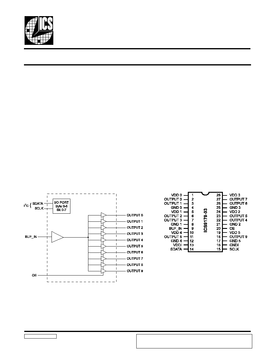
Block Diagram
PentiumPro is a trademark of Intel Corporation
I
2
C is a trademark of Philips Corporation
Low Skew Fan Out Buffers
9179-03 Rev H 10/16/00
Pin Configuration
The ICS9179-03 generates low skew clock buffers required
for high speed RISC or CISC microprocessor systems such as
Intel PentiumPro. Outputs will handle up to 133MHz clocks.
An output enable is provided for testability.
The device is a buffer with low output to output skew. This is
a Fanout buffer device, not using an internal PLL. This buffer
can also be a feedback to an external PLL stage for phase
synchronization to a master clock. There are a total of ten
outputs, sufficient for feedback to a PLL source and to drive
four small outline DIMM modules (S.O. DIMM) at 2 clocks
each. Or a total of ten outputs as a Fanout buffer from a
common clock source.
The individual clock outputs are addressable through I
2
C to
be enabled, or stopped in a low state for reduced EMI when
the lines are not needed.
Ten High speed, low noise non-inverting buffers for (to
133MHz), clock buffer applications.
Output slew rate faster than 1.5V/ns into 20pF
Supports up to four small outline DIMMS (S.O. DIMM).
Synchronous clocks skew matched to 250ps window on
OUTPUTs (0:9).
I
2
C Serial Configuration interface to allow individual
OUTPUTs to be stopped low.
Multiple VDD, VSS pins for noise reduction
Tri-state pin for testing
3.0V 3.7V supply range
28-pin (209 mil) SSOP and (6.1mm) TSSOP package
28-Pin SSOP & TSSOP
ICS reserves the right to make changes in the device data identified in this
publication without further notice. ICS advises its customers to obtain the latest
version of all device data to verify that any information being relied upon by the
customer is current and accurate.

2
ICS9179-03
Pin Descriptions
Power Groups
VDD (0:5), GND (0:5) = Power supply for OUTPUT buffer
VDDI, GNDI = Power supply for I
2
C circuitry
R
E
B
M
U
N
N
I
P
E
M
A
N
N
I
P
E
P
Y
T
N
O
I
T
P
I
R
C
S
E
D
3
,
2
)
1
:
0
(
T
U
P
T
U
O
T
U
O
s
t
u
p
t
u
o
k
c
o
l
C
1
0
D
N
G
,
0
D
D
V
s
e
s
u
,
7
,
6
)
3
:
2
(
T
U
P
T
U
O
T
U
O
s
t
u
p
t
u
o
k
c
o
l
C
1
1
D
N
G
,
1
D
D
V
s
e
s
u
,
3
2
,
2
2
)
5
:
4
(
T
U
P
T
U
O
T
U
O
s
t
u
p
t
u
o
k
c
o
l
C
1
2
D
N
G
,
2
D
D
V
s
e
s
u
7
2
,
6
2
)
7
:
6
(
T
U
P
T
U
O
T
U
O
t
u
p
t
u
o
k
c
o
l
C
1
3
D
N
G
,
3
D
D
V
s
e
s
u
1
1
8
T
U
P
T
U
O
T
U
O
t
u
p
t
u
o
k
c
o
l
C
1
4
D
N
G
,
4
D
D
V
s
e
s
u
8
1
9
T
U
P
T
U
O
T
U
O
t
u
p
t
u
o
k
c
o
l
C
1
5
D
N
G
,
5
D
D
V
s
e
s
u
9
N
I
_
F
U
B
N
I
s
r
e
f
f
u
b
r
o
f
t
u
p
n
I
0
2
E
O
N
I
.
p
u
-
l
l
u
p
l
a
n
r
e
t
n
i
s
a
H
.
W
O
L
d
l
e
h
n
e
h
w
s
t
u
p
t
u
o
l
l
a
s
e
t
a
t
s
-
i
r
T
2
4
1
A
T
A
D
S
O
/
I
I
r
o
f
n
i
p
a
t
a
D
2
y
r
t
i
u
c
r
i
c
C
3
5
1
K
L
C
S
O
/
I
I
r
o
f
n
i
p
k
c
o
l
C
2
y
r
t
i
u
c
r
i
c
C
3
,
0
1
,
5
,
1
8
2
,
4
2
,
9
1
)
5
:
0
(
D
D
V
R
W
P
s
r
e
f
f
u
b
T
U
P
T
U
O
r
o
f
y
l
p
p
u
s
r
e
w
o
P
V
3
.
3
,
2
1
,
8
,
4
5
2
,
1
2
,
7
1
,
6
1
)
5
:
0
(
D
N
G
R
W
P
s
r
e
f
f
u
b
T
U
P
T
U
O
r
o
f
d
n
u
o
r
G
3
1
I
D
D
V
R
W
P
I
r
o
f
y
l
p
p
u
s
r
e
w
o
P
V
3
.
3
2
c
i
g
o
l
l
a
n
r
e
t
n
i
d
n
a
y
r
t
i
u
c
r
i
c
C
6
1
I
D
N
G
R
W
P
I
r
o
f
d
n
u
o
r
G
2
c
i
g
o
l
l
a
n
r
e
t
n
i
d
n
a
y
r
t
i
u
c
r
i
c
C
Notes:
1.
At power up all ten OUTPUTs are enabled and active.
2.
OE has a 100K Ohm internal pull-up resistor to keep all outputs active.
3.
The SDATA and SCLK inputs both also have internal pull-up resistors with values above 100K Ohms as well for
complete platform flexibility.

3
ICS9179-03
VDD
This is the power supply to the internal core logic of the
device as well as the clock output buffers for OUTPUT (0:9).
This pin operates at 3.3V volts. Clocks from the listed buffers
that it supplies will have a voltage swing from Ground to this
level. For the actual guaranteed high and low voltage levels
for the Clocks, please consult the DC parameter table in this
data sheet.
GND
This is the power supply ground (common or negative) return
pin for the internal core logic and all the output buffers.
OUTPUT (0:9)
These Output Clocks are use to drive Dynamic RAMs and
are low skew copies of the CPU Clocks. The voltage swing of
the OUTPUTs output is controlled by the supply voltage
that is applied to VDD of the device, operates at 3.3 volts.
I
2
C
The SDATA and SCLOCK Inputs are use to program the
device. The clock generator is a slave-receiver device in the
I
2
C protocol. It will allow read-back of the registers. See
configuration map for register functions. The I
2
C specification
in Philips I
2
C Peripherals Data Handbook (1996) should be
followed.
BUF_IN
Input for Fanout buffers (OUTPUT 0:9).
OE
OE tristates all outputs when held low.
VDD1
This is the power supply to I
2
C circuitry.
Technical Pin Function Descriptions
4
ICS9179-03
1.
The ICS clock generator is a slave/receiver, I
2
C component. It can read back the data stored in the latches for verification.
Read-Back will support Intel PIIX4 "Block-Read" protocol.
2.
The data transfer rate supported by this clock generator is 100K bits/sec or less (standard mode)
3.
The input is operating at 3.3V logic levels.
4.
The data byte format is 8 bit bytes.
5.
To simplify the clock generator I
2
C interface, the protocol is set to use only "Block-Writes" from the controller. The
bytes must be accessed in sequential order from lowest to highest byte with the ability to stop after any complete byte
has been transferred. The Command code and Byte count shown above must be sent, but the data is ignored for those
two bytes. The data is loaded until a Stop sequence is issued.
6.
At power-on, all registers are set to a default condition, as shown.
General I
2
C serial interface information
The information in this section assumes familiarity with I
2
C programming.
For more information, contact ICS for an I
2
C programming application note.
How to Write:
Controller (host) sends a start bit.
Controller (host) sends the write address D2
(H)
ICS clock will acknowledge
Controller (host) sends a dummy command code
ICS clock will acknowledge
Controller (host) sends a dummy byte count
ICS clock will acknowledge
Controller (host) starts sending first byte (Byte 0)
through byte 5
ICS clock will acknowledge each byte one at a time.
Controller (host) sends a Stop bit
How to Read:
Controller (host) will send start bit.
Controler (host) sends the read address D3
(H)
ICS clock will acknowledge
ICS clock will send the byte count
Controller (host) acknowledges
ICS clock sends first byte (Byte 0) through byte 6
Controller (host) will need to acknowledge each byte
Controller (host) will send a stop bit
Notes:
Controller (Host)
ICS (Slave/Receiver)
Start Bit
Address
D2
(H)
ACK
Dummy Command Code
ACK
Dummy Byte Count
ACK
Byte 0
ACK
Byte 1
ACK
Byte 2
ACK
Byte 3
ACK
Byte 4
ACK
Byte 5
ACK
Byte 6
ACK
Stop Bit
How to Write:
Controller (Host)
ICS (Slave/Receiver)
Start Bit
Address
D3
(H)
ACK
Byte Count
ACK
Byte 0
ACK
Byte 1
ACK
Byte 2
ACK
Byte 3
ACK
Byte 4
ACK
Byte 5
ACK
Byte 6
ACK
Stop Bit
How to Read:
5
ICS9179-03
Byte 1: OUTPUT Clock Register
Notes: 1 = Enabled; 0 = Disabled, outputs held low
Byte 2: OUTPUT Clock Register
Notes: 1 = Enabled; 0 = Disabled, outputs held low
T
I
B
#
N
I
P
D
W
P
N
O
I
T
P
I
R
C
S
E
D
7
t
i
B
8
1
1
)
t
c
a
n
I
/
t
c
A
(
9
T
U
P
T
U
O
6
t
i
B
1
1
1
)
t
c
a
n
I
/
t
c
A
(
8
T
U
P
T
U
O
5
t
i
B
-
1
d
e
v
r
e
s
e
R
4
t
i
B
-
1
d
e
v
r
e
s
e
R
3
t
i
B
-
1
d
e
v
r
e
s
e
R
2
t
i
B
-
1
d
e
v
r
e
s
e
R
1
t
i
B
-
1
d
e
v
r
e
s
e
R
0
t
i
B
-
1
d
e
v
r
e
s
e
R
T
I
B
#
N
I
P
D
W
P
N
O
I
T
P
I
R
C
S
E
D
7
t
i
B
7
2
1
)
t
c
a
n
I
/
t
c
A
(
7
T
U
P
T
U
O
6
t
i
B
6
2
1
)
t
c
a
n
I
/
t
c
A
(
6
T
U
P
T
U
O
5
t
i
B
3
2
1
)
t
c
a
n
I
/
t
c
A
(
5
T
U
P
T
U
O
4
t
i
B
2
2
1
)
t
c
a
n
I
/
t
c
A
(
4
T
U
P
T
U
O
3
t
i
B
-
1
d
e
v
r
e
s
e
R
2
t
i
B
-
1
d
e
v
r
e
s
e
R
1
t
i
B
-
1
d
e
v
r
e
s
e
R
0
t
i
B
-
1
d
e
v
r
e
s
e
R
ICS9179-03 Power Management
The values below are estimates of target specifications.
Note: PWD = Power-Up Default
Serial Configuration Command Bitmaps
Byte 0: OUTPUT Clock Register (Default=0)
Notes: 1 = Enabled; 0 = Disabled, outputs held low
Note: PWD = Power-Up Default
T
I
B
#
N
I
P
D
W
P
N
O
I
T
P
I
R
C
S
E
D
7
t
i
B
-
1
d
e
v
r
e
s
e
R
6
t
i
B
-
1
d
e
v
r
e
s
e
R
5
t
i
B
-
1
d
e
v
r
e
s
e
R
4
t
i
B
-
1
d
e
v
r
e
s
e
R
3
t
i
B
7
1
3
T
U
P
T
U
O
2
t
i
B
6
1
2
T
U
P
T
U
O
1
t
i
B
3
1
1
T
U
P
T
U
O
0
t
i
B
2
1
0
T
U
P
T
U
O
Functionality
#
E
O
)
9
:
0
(
T
U
P
T
U
O
0
Z
-
i
H
1
N
I
_
F
U
B
X
1
n
o
i
t
i
d
n
o
C
n
o
i
t
p
m
u
s
n
o
c
y
l
p
p
u
s
V
3
.
3
x
a
M
s
d
a
o
l
p
a
c
e
t
e
r
c
s
i
d
x
a
M
V
5
6
4
.
3
=
D
D
V
D
N
G
r
o
D
D
V
=
s
t
u
p
n
i
c
i
t
a
t
s
l
l
A
e
d
o
M
k
c
o
l
C
o
N
)
D
N
G
r
o
1
D
D
V
-
N
I
_
F
U
B
(
I
2
e
v
i
t
c
A
y
r
t
i
u
c
r
i
C
C
A
m
3
z
H
M
6
6
e
v
i
t
c
A
)
z
H
M
6
6
.
6
6
=
N
I
_
F
U
B
(
A
m
0
3
2
z
H
M
0
0
1
e
v
i
t
c
A
)
z
H
M
0
0
.
0
0
1
=
N
I
_
F
U
B
(
A
m
0
6
3
z
H
M
3
3
1
e
v
i
t
c
A
)
z
H
M
3
3
.
3
3
1
=
N
I
_
F
U
B
(
A
m
0
6
4