Integrated
Circuit
Systems, Inc.
ICS932S202
0600A--08/04/03
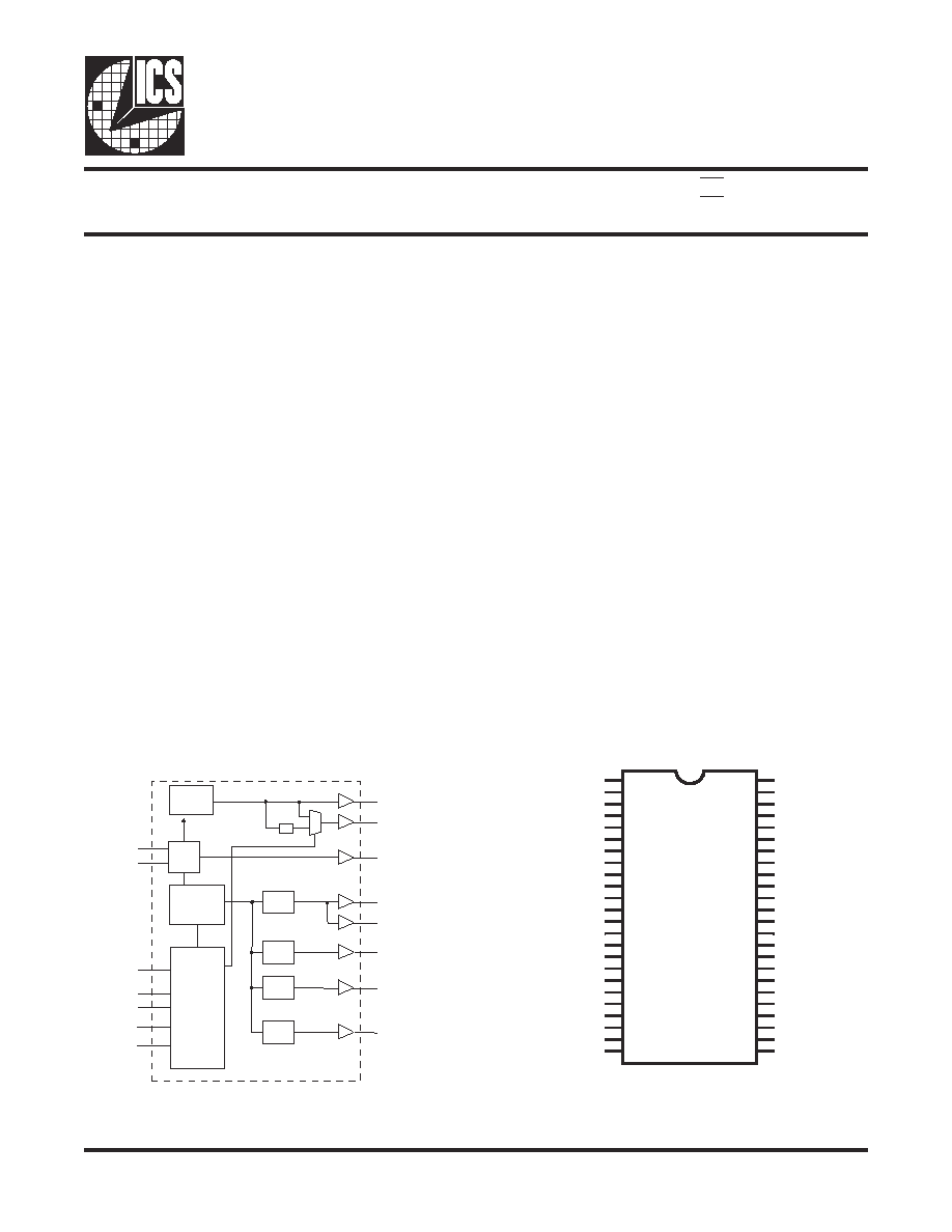
Block Diagram
Frequency Timing Generator for Differential PIII Type
Dual-CPU Systems
Pin Configuration
48-pin SSOP
*120K ohm pull-up to VDD on indicated inputs.
Recommended Application:
Serverwork HE-T, HE-SL & LE-T Chipsets
Output Features:
∑
2 - CPUs @ 2.5V, up to 180MHz
∑
2 - CPU chipset @ 2.5V, up to 180MHz
∑
3 - IOAPIC @ 2.5V
∑
3 - 3V66MHz @ 3.3V
∑
11 - PCIs @ 3.3V
∑
1 - 48MHz, @ 3.3V fixed
∑
1 - 24/48MHz, @ 3.3V
∑
2 - REF @ 3.3V
Features:
∑
Up to 180MHz frequency support
∑
Support power management: Power down Mode
from I
2
C programming.
∑
Spread spectrum for EMI control
± 0.25% center spread).
∑
Uses external 14.318MHz crystal
∑
5 - FS pins for frequency select
SEL24_48#
PLL2
PLL1
Spread
Spectrum
48MHz
24_48MHz
CPUCLK (1:0)
IOAPIC (2:0)
PCICLK (10:0)
CPU_CSCLK (1:0)
3V66 (2:0)
X1
X2
XTAL
OSC
CPU
DIVDER
IOAPIC
DIVDER
PCI
DIVDER
3V66
DIVDER
SDATA
SCLK
FS (4:0)
PD#
Control
Logic
Config.
Reg.
/ 2
REF (1:0)
GNDREF
REF0
*SEL24_48#/REF1
VDDREF
X1
X2
GNDPCI
*FS0/PCICLK0
*FS1/PCICLK1
VDDPCI
*FS2/PCICLK2
*FS3/PCICLK3
GNDPCI
PCICLK4
PCICLK5
VDDPCI
PCICLK6
PCICLK7
GNDPCI
PCICLK8
PCICLK9
PCICLK10
VDDPCI
PD#
ICS932S202
1
2
3
4
5
6
7
8
9
10
11
12
13
14
15
16
17
18
19
20
21
22
23
24
48
47
46
45
44
43
42
41
40
39
38
37
36
35
34
33
32
31
30
29
28
27
26
25
VDDLAPIC
IOAPIC0
IOAPIC1
GNDLAPIC
IOAPIC2
VDDLCPU
CPUCLK0
GNDLCPU
CPUCLK1
VDDLCPU
CPU_CSCLK0
CPU_CSCLK1
GNDLCPU
VDD66
3V66_0
3V66_1
3V66_2
GND66
SDATA
SCLK
VDD48
48MHz/FS4*
24_48MHz
GND48
Key Specifications:
∑
CPU Output Jitter: <150ps
∑
IOAPIC Output Jitter: <500ps
∑
48MHz, 3V66, PCI Output Jitter: <500ps
∑
Ref Output Jitter. <1000ps
∑
CPU Output Skew: <175ps
∑
IOAPIC Output Skew <250ps
∑
PCI Output Skew: <500ps
∑
3V66 Output Skew <250ps
∑
CPU to 3V66 Output Offset: 0.8 - 1.8ns (typ =
1.3ns)
∑
CPU to PCI Output Offset: 0.0 - 1.5ns (typ =
0.9ns)
∑
CPU to IOAPIC Output Offset: 1.5 - 4.0ns (typ =
2.0ns)
2
ICS932S202
0600A--08/04/03
Pin Descriptions
The ICS932S202 is a main clock synthesizer chip for Pentium II based systems using Rambus Interface DRAMs. This
chip provides all the clocks required for such a system.
Spread Spectrum may be enabled through I
2
C. Spread spectrum typically reduces system EMI by 8dB to 10dB. This
simplifies EMI qualification without resorting to board design iterations or costly shielding. The ICS932S202 employs
a proprietary closed loop design, which tightly controls the percentage of spreading over process and temperature
variations.
General Description
Pin number
Pin name
Type
Description
1, 7, 13, 19, 25,
31, 36, 41, 45
GND
PWR
Ground pins
2
REF0
OUT
14.318MHz reference clock outputs at 3.3V
REF1
OUT
14.318MHz reference clock outputs at 3.3V
SEL24_48
IN
Logic input to select 24 or 48MHz for pin 26 output
4, 10, 16, 23,
28, 35
VDD
PWR
Power pins 3.3V
5
X1
IN
XTAL_IN 14.318MHz crystal input
6
X2
OUT
XTAL_OUT Crystal output
PCICLK0
OUT
PCI clock output at 3.3V. Synchronous to CPU clocks.
FS0
IN
Logic - input for frequency selection
PCICLK1
OUT
PCI clock output at 3.3V. Synchronous to CPU clocks.
FS1
IN
Logic - input for frequency selection
PCICLK2
OUT
PCI clock output at 3.3V. Synchronous to CPU clocks.
FS2
IN
Logic - input for frequency selection
PCICLK3
OUT
PCI clock output at 3.3V. Synchronous to CPU clocks.
FS3
IN
Logic - input for frequency selection
22, 21, 20, 18,
17, 15, 14
PCICLK (10:4)
OUT
PCI clock outputs at 3.3V. Synchronous to CPU clocks.
24
PD#
IN
This asynchronous input powers down the chip when drive
active(Low). The internal PLLs are disabled and all the
output clocks are held at a Low state.
26
24_48MHz
OUT
24 or 48MHz output selectable by
SEL24_48# (0=48MHz 1=24MHz)
48MHz
OUT/IN
Fixed 48MHz clock output. 3.3V
FS4
IN
Logic - input for frequency selection
29
SCLK
IN
Clock input of I
2
C input
30
SDATA
I/O
Data pin for I
2
C circuitry 5V tolerant
34, 33, 32
3V66 (2:0)
OUT
3.3V clock outputs. These outputs are stopped when
CPU_STOP# is driven active..
38, 37
CPU_CSCLK (1:0)
OUT
Chipset clock outputs @ 2.5V
40, 42
CPUCLK (1:0)
OUT
CPU clock outputs @ 2.5V.
39, 43
VDDLCPU
PWR
Power pins for CPUCLKs. 2.5V
44, 46, 47
IOAPIC (2:0)
OUT
IOAPIC clocks @ 2.5V. Synchronous with CPUCLKs.
48
VDDLAPIC
PWR
Power pin for the IOAPIC outputs. 2.5V.
27
12
3
8
9
11
3
ICS932S202
0600A--08/04/03
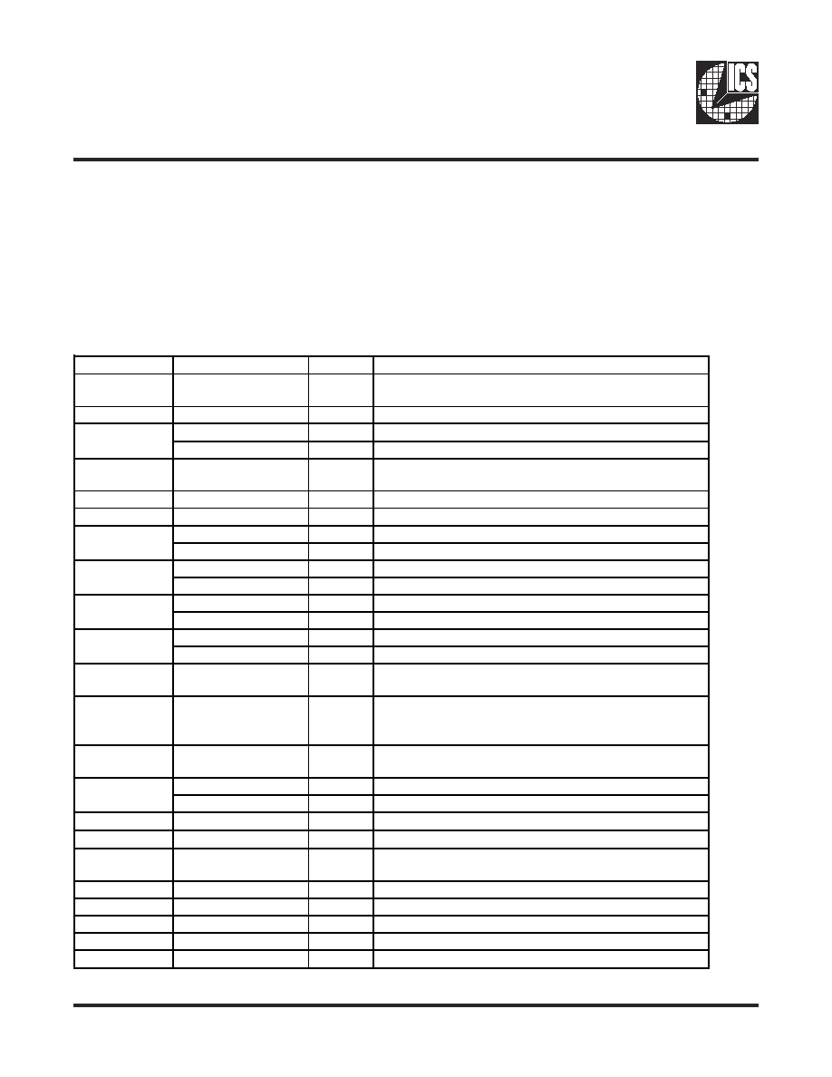
Functionality
FS4
FS3
FS2
FS1
FS0
CPU
PCI
3V66
IOAPIC
0
0
0
0
0
103.0
34.33
68.67
17.17
0
0
0
0
1
100.0
33.33
66.67
16.67
0
0
0
1
0
100.45
33.48
66.97
16.74
0
0
0
1
1
100.9
33.63
67.27
16.82
0
0
1
0
0
107.1
35.70
71.40
17.85
0
0
1
0
1
109.0
36.33
72.67
18.17
0
0
1
1
0
112.0
37.33
74.67
18.67
0
0
1
1
1
114.00
28.50
57.00
14.25
0
1
0
0
0
116.00
29.00
58.00
14.50
0
1
0
0
1
118.00
29.50
59.00
14.75
0
1
0
1
0
133.30
33.33
66.65
16.66
0
1
0
1
1
120.00
30.00
60.00
15.00
0
1
1
0
0
122.00
30.50
61.00
15.25
0
1
1
0
1
125.00
31.25
62.50
15.63
0
1
1
1
0
50.0
16.67
33.33
8.33
0
1
1
1
1
66.7
16.67
33.33
8.33
1
0
0
0
0
133.3
33.33
66.67
16.67
1
0
0
0
1
133.9
33.48
66.95
16.74
1
0
0
1
0
138.0
34.50
69.00
17.25
1
0
0
1
1
142.0
35.50
71.00
17.75
1
0
1
0
0
146.0
36.50
73.00
18.25
1
0
1
0
1
150.0
37.50
75.00
18.75
1
0
1
1
0
153.0
38.25
76.50
19.13
1
0
1
1
1
156.0
39.00
78.00
19.50
1
1
0
0
0
159.1
39.78
79.55
19.89
1
1
0
0
1
162.0
40.50
81.00
20.25
1
1
0
1
0
166.7
41.67
83.33
20.83
1
1
0
1
1
168.0
42.00
84.00
21.00
1
1
1
0
0
171.0
42.75
85.50
21.38
1
1
1
0
1
174.0
43.50
87.00
21.75
1
1
1
1
0
177.0
44.25
88.50
22.13
1
1
1
1
1
180.0
45.00
90.00
22.50

4
ICS932S202
0600A--08/04/03
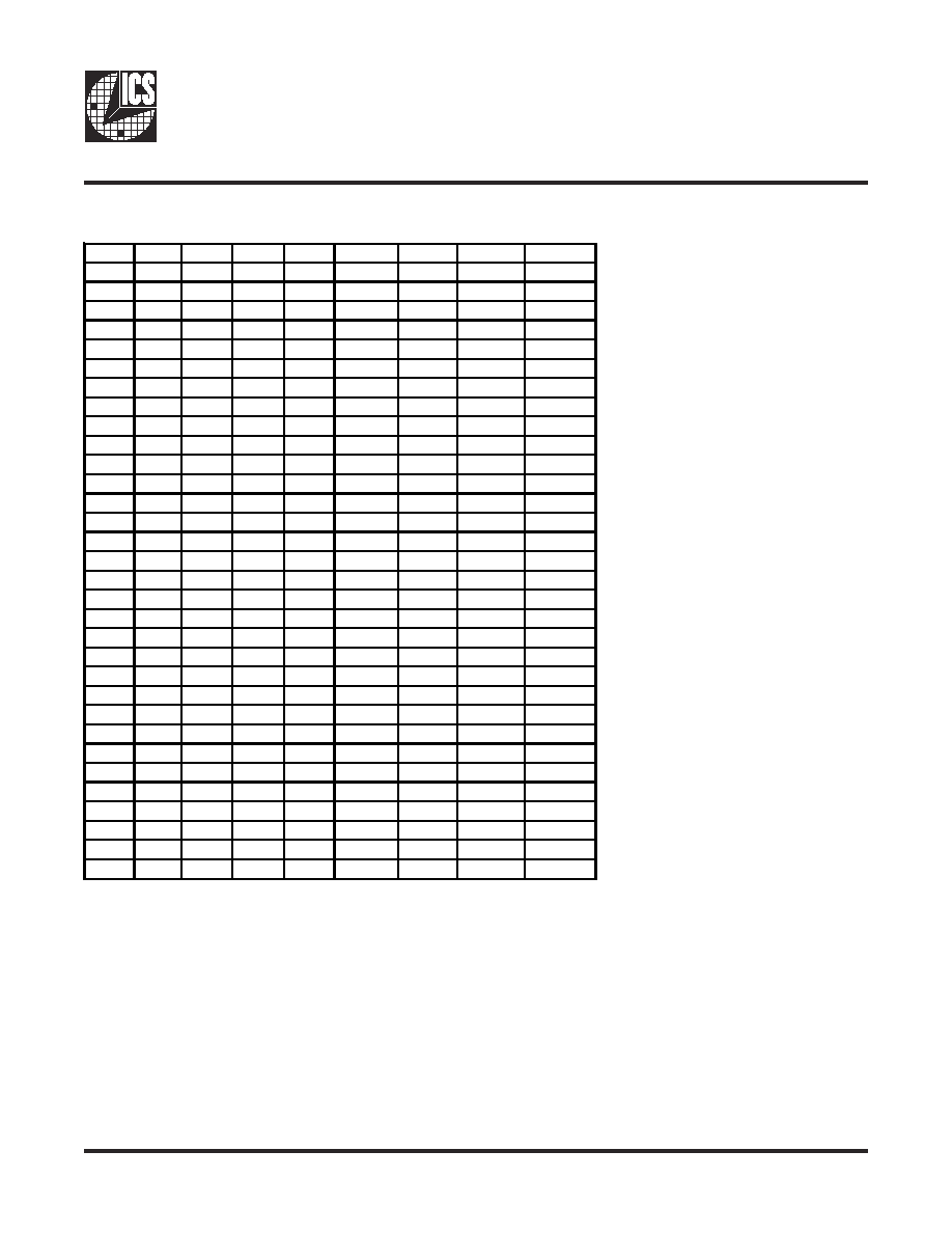
Byte 0: Functionality and frequency select register (Default = 0)
Serial Configuration Command Bitmap
Note 1:
Default at power-up will be for latched logic inputs to define frequency, as displayed byBit 3.
t
i
B
n
o
i
t
p
i
r
c
s
e
D
D
W
P
t
i
B
)
4
:
7
,
2
(
2
t
i
B
4
S
F
7
t
i
B
3
S
F
6
t
i
B
2
S
F
5
t
i
B
1
S
F
4
t
i
B
0
S
F
U
P
C
I
C
P
6
6
V
3
C
I
P
A
O
I
d
e
v
r
e
s
e
R
1
e
t
o
N
0
0
0
0
0
0
.
3
0
1
3
3
.
4
3
7
6
.
8
6
7
1
.
7
1
0
0
0
0
1
0
.
0
0
1
3
3
.
3
3
7
6
.
6
6
7
6
.
6
1
0
0
0
1
0
5
4
.
0
0
1
8
4
.
3
3
7
9
.
6
6
4
7
.
6
1
0
0
0
1
1
9
.
0
0
1
3
6
.
3
3
7
2
.
7
6
2
8
.
6
1
0
0
1
0
0
1
.
7
0
1
0
7
.
5
3
0
4
.
1
7
5
8
.
7
1
0
0
1
0
1
0
.
9
0
1
3
3
.
6
3
7
6
.
2
7
7
1
.
8
1
0
0
1
1
0
0
.
2
1
1
3
3
.
7
3
7
6
.
4
7
7
6
.
8
1
0
0
1
1
1
0
0
.
4
1
1
0
5
.
8
2
0
0
.
7
5
5
2
.
4
1
0
1
0
0
0
0
0
.
6
1
1
0
0
.
9
2
0
0
.
8
5
0
5
.
4
1
0
1
0
0
1
0
0
.
8
1
1
0
5
.
9
2
0
0
.
9
5
5
7
.
4
1
0
1
0
1
0
0
3
.
3
3
1
3
3
.
3
3
5
6
.
6
6
6
6
.
6
1
0
1
0
1
1
0
0
.
0
2
1
0
0
.
0
3
0
0
.
0
6
0
0
.
5
1
0
1
1
0
0
0
0
.
2
2
1
0
5
.
0
3
0
0
.
1
6
5
2
.
5
1
0
1
1
0
1
0
0
.
5
2
1
5
2
.
1
3
0
5
.
2
6
3
6
.
5
1
0
1
1
1
0
0
.
0
5
7
6
.
6
1
3
3
.
3
3
3
3
.
8
0
1
1
1
1
7
.
6
6
7
6
.
6
1
3
3
.
3
3
3
3
.
8
1
0
0
0
0
3
.
3
3
1
3
3
.
3
3
7
6
.
6
6
7
6
.
6
1
1
0
0
0
1
9
.
3
3
1
8
4
.
3
3
5
9
.
6
6
4
7
.
6
1
1
0
0
1
0
0
.
8
3
1
0
5
.
4
3
0
0
.
9
6
5
2
.
7
1
1
0
0
1
1
0
.
2
4
1
0
5
.
5
3
0
0
.
1
7
5
7
.
7
1
1
0
1
0
0
0
.
6
4
1
0
5
.
6
3
0
0
.
3
7
5
2
.
8
1
1
0
1
0
1
0
.
0
5
1
0
5
.
7
3
0
0
.
5
7
5
7
.
8
1
1
0
1
1
0
0
.
3
5
1
5
2
.
8
3
0
5
.
6
7
3
1
.
9
1
1
0
1
1
1
0
.
6
5
1
0
0
.
9
3
0
0
.
8
7
0
5
.
9
1
1
1
0
0
0
1
.
9
5
1
8
7
.
9
3
5
5
.
9
7
9
8
.
9
1
1
1
0
0
1
0
.
2
6
1
0
5
.
0
4
0
0
.
1
8
5
2
.
0
2
1
1
0
1
0
7
.
6
6
1
7
6
.
1
4
3
3
.
3
8
3
8
.
0
2
1
1
0
1
1
0
.
8
6
1
0
0
.
2
4
0
0
.
4
8
0
0
.
1
2
1
1
1
0
0
0
.
1
7
1
5
7
.
2
4
0
5
.
5
8
8
3
.
1
2
1
1
1
0
1
0
.
4
7
1
0
5
.
3
4
0
0
.
7
8
5
7
.
1
2
1
1
1
1
0
0
.
7
7
1
5
2
.
4
4
0
5
.
8
8
3
1
.
2
2
1
1
1
1
1
0
.
0
8
1
0
0
.
5
4
0
0
.
0
9
0
5
.
2
2
3
t
i
B
s
t
u
p
n
i
d
e
h
c
t
a
l
,
t
c
e
l
e
s
e
r
a
w
d
r
a
h
y
b
d
e
t
c
e
l
e
s
s
i
y
c
n
e
u
q
e
r
F
-
0
4
:
7
,
2
t
i
B
y
b
d
e
t
c
e
l
e
s
s
i
y
c
n
e
u
q
e
r
F
-
1
0
1
t
i
B
l
a
m
r
o
N
-
0
d
e
l
b
a
n
e
m
u
r
t
c
e
p
s
d
a
e
r
p
S
-
1
1
0
t
i
B
g
n
i
n
n
u
R
-
0
s
t
u
p
t
u
o
ll
a
e
t
a
t
s
i
r
T
-
1
0

5
ICS932S202
0600A--08/04/03
Byte 1: CPU, Active/Inactive
Register (1 = enable, 0 = disable)
Byte 2: PCI Active/Inactive
Register (1 = enable, 0 = disable)
Byte 3: 3V66 Active/Inactive Register
(1 = enable, 0 = disable)
Notes:
1. Inactive means outputs are held LOW and are disabled
from switching.
Notes:
1. Inactive means outputs are held LOW and are disabled
from switching.
Notes:
1. Inactive means outputs are held LOW and are disabled
from switching.
Byte 4: PCI Active/Inactive Register
(1 = enable, 0 = disable)
Notes:
1. Inactive means outputs are held LOW and are
disabled from switching.
t
i
B
#
n
i
P
D
W
P
n
o
i
t
p
i
r
c
s
e
D
7
t
i
B
0
4
1
1
K
L
C
U
P
C
6
t
i
B
8
3
1
0
K
L
C
S
C
U
P
C
5
t
i
B
7
3
1
1
K
L
C
S
C
U
P
C
4
t
i
B
2
4
1
0
K
L
C
U
P
C
3
t
i
B
7
4
1
0
C
I
P
A
O
I
2
t
i
B
6
4
1
1
C
I
P
A
O
I
1
t
i
B
4
4
1
2
C
I
P
A
O
I
0
t
i
B
-
X
)
d
e
v
r
e
s
e
R
(
t
i
B
#
n
i
P
D
W
P
n
o
i
t
p
i
r
c
s
e
D
7
t
i
B
8
1
1
7
K
L
C
I
C
P
6
t
i
B
7
1
1
6
K
L
C
I
C
P
5
t
i
B
5
1
1
5
K
L
C
I
C
P
4
t
i
B
4
1
1
4
K
L
C
I
C
P
3
t
i
B
2
1
1
3
K
L
C
I
C
P
2
t
i
B
1
1
1
2
K
L
C
I
C
P
1
t
i
B
9
1
1
K
L
C
I
C
P
0
t
i
B
8
1
0
K
L
C
I
C
P
t
i
B
#
n
i
P
D
W
P
n
o
i
t
p
i
r
c
s
e
D
7
t
i
B
4
3
1
0
_
6
6
V
3
6
t
i
B
3
3
1
1
_
6
6
V
3
5
t
i
B
2
3
1
2
_
6
6
V
3
4
t
i
B
-
X
#
1
S
F
3
t
i
B
2
1
0
F
E
R
2
t
i
B
3
1
1
F
E
R
1
t
i
B
-
X
#
3
S
F
0
t
i
B
-
X
#
2
S
F
t
i
B
#
n
i
P
D
W
P
n
o
i
t
p
i
r
c
s
e
D
7
t
i
B
6
2
1
z
H
M
8
4
_
4
2
6
t
i
B
7
2
1
z
H
M
8
4
5
t
i
B
-
X
#
0
S
F
4
t
i
B
-
1
)
d
e
v
r
e
s
e
R
(
3
t
i
B
2
2
1
0
1
K
L
C
I
C
P
2
t
i
B
1
2
1
9
K
L
C
I
C
P
1
t
i
B
0
2
1
8
K
L
C
I
C
P
0
t
i
B
-
X
#
4
S
F
Byte 5: Active/Inactive Register
(1= enable, 0 = disable)
t
i
B
#
n
i
P
D
W
P
n
o
i
t
p
i
r
c
s
e
D
7
t
i
B
-
0
)
e
t
o
N
(
d
e
v
r
e
s
e
R
6
t
i
B
-
0
)
e
t
o
N
(
d
e
v
r
e
s
e
R
5
t
i
B
-
0
)
e
t
o
N
(
d
e
v
r
e
s
e
R
4
t
i
B
-
0
)
e
t
o
N
(
d
e
v
r
e
s
e
R
3
t
i
B
-
0
)
e
t
o
N
(
d
e
v
r
e
s
e
R
2
t
i
B
-
1
)
e
t
o
N
(
d
e
v
r
e
s
e
R
1
t
i
B
-
1
)
e
t
o
N
(
d
e
v
r
e
s
e
R
0
t
i
B
-
0
)
e
t
o
N
(
d
e
v
r
e
s
e
R
Byte6: Active/Inactive Register
(1= enable, 0 = disable)
Note: Don't write into this register, writing into this
register can cause malfunction
t
i
B
#
n
i
P
D
W
P
n
o
i
t
p
i
r
c
s
e
D
7
t
i
B
-
1
)
e
t
o
N
(
d
e
v
r
e
s
e
R
6
t
i
B
-
1
)
e
t
o
N
(
d
e
v
r
e
s
e
R
5
t
i
B
-
1
)
e
t
o
N
(
d
e
v
r
e
s
e
R
4
t
i
B
-
1
)
e
t
o
N
(
d
e
v
r
e
s
e
R
3
t
i
B
-
1
)
e
t
o
N
(
d
e
v
r
e
s
e
R
2
t
i
B
-
1
)
e
t
o
N
(
d
e
v
r
e
s
e
R
1
t
i
B
-
1
)
e
t
o
N
(
d
e
v
r
e
s
e
R
0
t
i
B
-
1
)
e
t
o
N
(
d
e
v
r
e
s
e
R
Notes:
1. Inactive means outputs are held LOW and are disabled
from switching.