Integrated
Circuit
Systems, Inc.
ICS950810
0472F--01/12/04
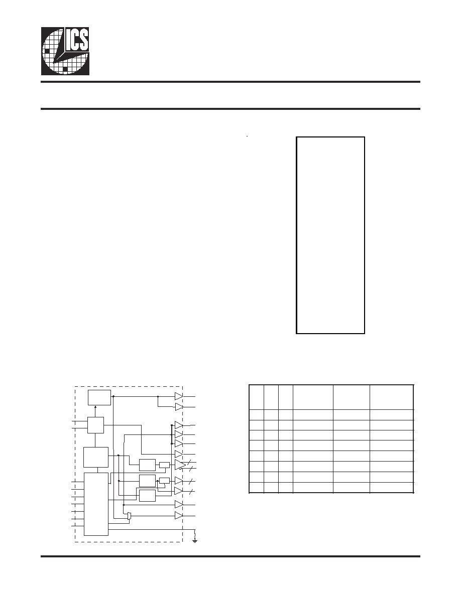
Block Diagram
Recommended Application:
CK-408 clock for BANIAS processor/ ODEM and
MONTARA-G chipsets.
Output Features:
∑
3 Differential CPU Clock Pairs @ 3.3V
∑
7 PCI (3.3V) @ 33.3MHz
∑
3 PCI_F (3.3V) @ 33.3MHz
∑
1 USB (3.3V) @ 48MHz
∑
1 DOT (3.3V) @ 48MHz
∑
1 REF (3.3V) @ 14.318MHz
∑
5 3V66 (3.3V) @ 66.6MHz
∑
1 VCH/3V66 (3.3V) @ 48MHz or 66.6MHz
Features:
∑
Supports spread spectrum modulation,
down spread 0 to -0.5%. (CPU, 3V66, PCI)
∑
Efficient power management scheme through PD#,
CPU_STOP# and PCI_STOP#.
Key Specifications:
∑
CPU Output Jitter <150ps
∑
3V66 Output Jitter <250ps
∑
CPU Output Skew <100ps
Pin Configuration
56-Pin 300mil SSOP
6.10 mm. Body, 0.50 mm. pitch TSSOP
Frequency Generator with 200MHz Differential CPU Clocks
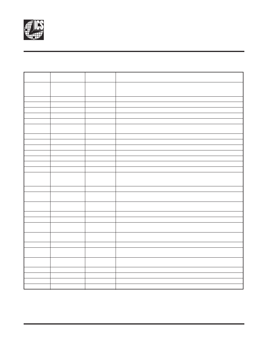
Functionality
* These inputs have 150K internal pull-up resistor to VDD.
2
S
F
1
S
F
0
S
F
U
P
C
)
z
H
M
(
)
0
:
5
(
6
6
V
3
)
z
H
M
(
F
_
I
C
P
I
C
P
)
z
H
M
(
X
0
0
6
6
.
6
6
1
6
6
.
6
6
3
3
.
3
3
X
0
1
0
0
.
0
0
1
6
6
.
6
6
3
3
.
3
3
X
1
0
0
0
.
0
0
2
6
6
.
6
6
3
3
.
3
3
X
1
1
3
3
.
3
3
1
6
6
.
6
6
3
3
.
3
3
d
i
M
0
0
e
t
a
t
s
i
r
T
e
t
a
t
s
i
r
T
e
t
a
t
s
i
r
T
d
i
M
0
1
2
/
K
L
C
T
4
/
K
L
C
T
8
/
K
L
C
T
d
i
M
1
0
d
e
v
r
e
s
e
R
d
e
v
r
e
s
e
R
d
e
v
r
e
s
e
R
d
i
M
1
1
d
e
v
r
e
s
e
R
d
e
v
r
e
s
e
R
d
e
v
r
e
s
e
R
PLL2
PLL1
Spread
Spectrum
3V66_5
3V66_3
3V66_(4,2)
48MHz_USB
48MHz_DOT
X1
X2
XTAL
OSC
3V66
DIVDER
PD#
CPU_STOP#
PCI_STOP#
MULTSEL0
SDATA
SCLK
FS (2:0)
I REF
Control
Logic
Config.
Reg.
REF
3V66_0
CPU
DIVDER
3
3
CPUCLKT (2:0)
CPUCLKC (2:0)
Stop
3V66_1/VCH_CLK
PCICLK (6:0)
PCI
DIVDER
3
7
PCICLK_F (2:0)
Stop
VDDREF
1
56 REF
X1
2
55 FS1
X2
3
54 FS0
GND
4
53 CPU_STOP#*
PCICLK_F0
5
52 CPUCLKT0
PCICLK_F1
6
51 CPUCLKC0
PCICLK_F2
7
50 VDDCPU
VDDPCI
8
49 CPUCLKT1
GND
9
48 CPUCLKC1
PCICLK0 10
47 GND
PCICLK1 11
46 VDDCPU
PCICLK2 12
45 CPUCLKT2
PCICLK3 13
44 CPUCLKC2
VDDPCI 14
43 MULTSEL0*
GND 15
42 IREF
PCICLK4 16
41 GND
PCICLK5 17
40 FS2
PCICLK6 18
39 48MHz_USB
VDD3V66 19
38 48MHz_DOT
GND 20
37 VDD48
3V66_2 21
36 GND
3V66_3 22
35 3V66_1/VCH_CLK
3V66_4 23
34 PCI_STOP#*
3V66_5 24
33 3V66_0
*PD# 25
32 VDD3V66
VDDA 26
31 GND
GND 27
30 SCLK
Vtt_PWRGD# 28
29 SDATA
I
C
S950810

4
ICS950810
0472F--01/12/04
Host Swing Select Functions
0
L
E
S
I
T
L
U
M
t
e
g
r
a
T
d
r
a
o
B
Z
m
r
e
T
/
e
c
a
r
T
,
R
e
c
n
e
r
e
f
e
R
=
f
e
r
I
V
D
D
)
r
R
*
3
(
/
t
u
p
t
u
O
t
n
e
r
r
u
C
Z
@
h
o
V
0
-
-
-
-
1
s
m
h
o
0
5
,
%
1
5
7
4
=
r
R
A
m
2
3
.
2
=
f
e
r
I
F
E
R
I
*
6
=
h
o
I
0
5
@
V
7
.
0
Truth Table
Maximum Allowed Current
n
o
i
t
i
d
n
o
C
n
o
i
t
p
m
u
s
n
o
c
y
l
p
p
u
s
V
3
.
3
x
a
M
,
s
d
a
o
l
p
a
c
e
t
e
r
c
s
i
d
x
a
M
V
5
6
4
.
3
=
d
d
V
D
N
G
r
o
d
d
V
=
s
t
u
p
n
i
c
i
t
a
t
s
ll
A
e
d
o
M
n
w
o
d
r
e
w
o
P
)
0
=
#
N
W
D
R
W
P
(
A
m
5
2
e
v
i
t
c
A
l
l
u
F
A
m
0
6
3
2
S
F
1
S
F
0
S
F
U
P
C
)
z
H
M
(
6
6
V
3
)
0
:
5
(
)
z
H
M
(
F
_
I
C
P
I
C
P
)
z
H
M
(
0
F
E
R
)
z
H
M
(
T
O
D
/
B
S
U
)
z
H
M
(
X
0
0
6
6
.
6
6
1
6
6
.
6
6
3
3
.
3
3
8
1
3
.
4
1
0
0
.
8
4
X
0
1
0
0
.
0
0
1
6
6
.
6
6
3
3
.
3
3
8
1
3
.
4
1
0
0
.
8
4
X
1
0
0
0
.
0
0
2
6
6
.
6
6
3
3
.
3
3
8
1
3
.
4
1
0
0
.
8
4
X
1
1
3
3
.
3
3
1
6
6
.
6
6
3
3
.
3
3
8
1
3
.
4
1
0
0
.
8
4
d
i
M
0
0
e
t
a
t
s
i
r
T
e
t
a
t
s
i
r
T
e
t
a
t
s
i
r
T
e
t
a
t
s
i
r
T
e
t
a
t
s
i
r
T
d
i
M
0
1
2
/
K
L
C
T
4
/
K
L
C
T
8
/
K
L
C
T
K
L
C
T
2
/
K
L
C
T
d
i
M
1
0
d
e
v
r
e
s
e
R
d
e
v
r
e
s
e
R
d
e
v
r
e
s
e
R
d
e
v
r
e
s
e
R
d
e
v
r
e
s
e
R
d
i
M
1
1
d
e
v
r
e
s
e
R
d
e
v
r
e
s
e
R
d
e
v
r
e
s
e
R
d
e
v
r
e
s
e
R
d
e
v
r
e
s
e
R
Power Groups
(Analog)
VDDA = PLL1
VDD48 = 48MHz, PLL
VDDREF = VDD for Xtal, POR
(Digital)
VDDPCI
VDD3V66
VDDCPU
NOTE: MULTSEL0 = 0 not supported in ICS950810. Refer to ICS950805 for Buffered Mode support.