 | –≠–ª–µ–∫—Ç—Ä–æ–Ω–Ω—ã–π –∫–æ–º–ø–æ–Ω–µ–Ω—Ç: ICS954101 | –°–∫–∞—á–∞—Ç—å:  PDF PDF  ZIP ZIP |

Integrated
Circuit
Systems, Inc.
ICS954101
0815D--06/21/04
Pin Configuration
Recommended Application:
CK410 clock, Intel Yellow Cover part
Output Features:
∑
2 - 0.7V current-mode differential CPU pairs
∑
6 - 0.7V current-mode differential SRC pair for SATA and
PCI-E
∑
1 - 0.7V current-mode differential CPU/SRC selectable
pair
∑
6 - PCI (33MHz)
∑
3 - PCICLK_F, (33MHz) free-running
∑
1 - USB, 48MHz
∑
1 - DOT, 96MHz, 0.7V current differential pair
∑
1 - REF, 14.318MHz
Key Specifications:
∑
CPU outputs cycle-cycle jitter < 85ps
∑
SRC output cycle-cycle jitter <125ps
∑
PCI outputs cycle-cycle jitter < 500ps
∑
+/- 300ppm frequency accuracy on CPU & SRC clocks
Programmable Timing Control HubTM for Desktop P4TM Systems
Functionality
Features/Benefits:
∑
Supports tight ppm accuracy clocks for Serial-ATA and
PCI-Express
∑
Supports spread spectrum modulation, 0 to -0.5%
down spread
∑
Supports CPU clks up to 400MHz
∑
Uses external 14.318MHz crystal, external crystal load
caps are required for frequency tuning
∑
Supports undriven differential CPU, SRC pair in PD#
for power management.
56-pin SSOP & TSSOP
VDDPCI 1
56 PCICLK2
GND 2
55 PCICLK1
PCICLK3 3
54 PCICLK0
PCICLK4 4
53 FS_C/TEST_SEL
PCICLK5 5
52 REFOUT
GND 6
51 GND
VDDPCI 7
50 X1
ITP_EN/PCICLK_F0 8
49 X2
PCICLK_F1 9
48 VDDREF
PCICLK_F2 10
47 SDATA
VDD48 11
46 SCLK
USB_48MHz 12
45 GND
GND 13
44 CPUCLKT0
DOTT_96MHz 14
43 CPUCLKC0
DOTC_96MHz 15
42 VDDCPU
FS_B/TEST_MODE 16
41 CPUCLKT1
Vtt_PwrGd#/PD 17
40 CPUCLKC1
FS_A_410 18
39 IREF
SRCCLKT1 19
38 GNDA
SRCCLKC1 20
37 VDDA
VDDSRC 21
36 CPUCLKT2_ITP/SRCCLKT_7
SRCCLKT2 22
35 CPUCLKC2_ITP/SRCCLKC_7
SRCCLKC2 23
34 VDDSRC
SRCCLKT3 24
33 SRCCLKT6
SRCCLKC3 25
32 SRCCLKC6
SRCCLKT4_SATA 26
31 SRCCLKT5
SRCCLKC4_SATA 27
30 SRCCLKC5
VDDSRC 28
29 GND
I
C
S95
410
1
FS_C
1
FS_B
2
FS_A
2
CPU
MHz
SRC
MHz
PCI
MHz
REF
MHz
U
SB
MHz
DOT
MHz
0
0
0
266.66
100.00
33.33 14.318
48.00
96.00
0
0
1
133.33
100.00
33.33 14.318
48.00
96.00
0
1
0
200.00
100.00
33.33 14.318
48.00
96.00
0
1
1
166.66
100.00
33.33 14.318
48.00
96.00
1
0
0
333.33
100.00
33.33 14.318
48.00
96.00
1
0
1
100.00
100.00
33.33 14.318
48.00
96.00
1
1
0
400.00
100.00
33.33 14.318
48.00
96.00
1
1
1
14.318
48.00
96.00
1. FS_C is a three-level input. Please see V
IL_FS
and V
IH_FS
specifications in
the Input/Supply/Common Output Parameters Table for correct values.
Also refer to the Test Clarification Table.
2. FS_B and FS_A are low-threshold inputs. Please see the V
IL_FS
and V
IH_FS
specifications in the Input/Supply/Common Output Parameters Table for correct values.
RESERVED

2
Integrated
Circuit
Systems, Inc.
ICS954101
0815D--06/21/04
Pin Description
Pin #
PIN NAME
PIN TYPE
DESCRIPTION
1
VDDPCI
PWR
Power supply for PCI clocks, nominal 3.3V
2
GND
PWR
Ground pin.
3
PCICLK3
OUT
PCI clock output.
4
PCICLK4
OUT
PCI clock output.
5
PCICLK5
OUT
PCI clock output.
6
GND
PWR
Ground pin.
7
VDDPCI
PWR
Power supply for PCI clocks, nominal 3.3V
8
ITP_EN/PCICLK_F0
I/O
Free running PCI clock not affected by PCI_STOP#.
ITP_EN: latched input to select pin functionality
1 = CPU_ITP pair
0 = SRC pair
9
PCICLK_F1
OUT
Free running PCI clock not affected by PCI_STOP# .
10
PCICLK_F2
OUT
Free running PCI clock not affected by PCI_STOP# .
11
VDD48
PWR
Power pin for the 48MHz output.3.3V
12
USB_48MHz
OUT
48.00MHz USB clock
13
GND
PWR
Ground pin.
14
DOTT_96MHz
OUT
True clock of differential pair for 96.00MHz DOT clock.
15
DOTC_96MHz
OUT
Complement clock of differential pair for 96.00MHz DOT clock.
16
FS_B/TEST_MODE
IN
3.3V tolerant input for CPU frequency selection. Refer to input electrical
characteristics for Vil_FS and Vih_FS values. TEST_MODE is a real time
input to select between Hi-Z and REF/N divider mode while in test mode.
Refer to Test Clarification Table.
17
Vtt_PwrGd#/PD
IN
Vtt_PwrGd# is an active low input used to determine when latched inputs
are ready to be sampled. PD is an asynchronous active high input pin
used to put the device into a low power state. The internal clocks, PLLs
and the crystal oscillator are stopped.
18
FS_A_410
IN
3.3V tolerant low threshold input for CPU frequency selection. This pin
requires CK410 FSA. Refer to input electrical characteristics for Vil_FS
and Vih_FS threshold values.
19
SRCCLKT1
OUT
True clock of differential SRC clock pair.
20
SRCCLKC1
OUT
Complement clock of differential SRC clock pair.
21
VDDSRC
PWR
Supply for SRC clocks, 3.3V nominal
22
SRCCLKT2
OUT
True clock of differential SRC clock pair.
23
SRCCLKC2
OUT
Complement clock of differential SRC clock pair.
24
SRCCLKT3
OUT
True clock of differential SRC clock pair.
25
SRCCLKC3
OUT
Complement clock of differential SRC clock pair.
26
SRCCLKT4_SATA
OUT
True clock of differential SRC/SATA pair.
27
SRCCLKC4_SATA
OUT
Complement clock of differential SRC/SATA pair.
28
VDDSRC
PWR
Supply for SRC clocks, 3.3V nominal

3
Integrated
Circuit
Systems, Inc.
ICS954101
0815D--06/21/04
Pin Description (Continued)
Pin #
PIN NAME
TYPE
DESCRIPTION
29
GND
PWR
Ground pin.
30
SRCCLKC5
OUT
Complement clock of differential SRC clock pair.
31
SRCCLKT5
OUT
True clock of differential SRC clock pair.
32
SRCCLKC6
OUT
Complement clock of differential SRC clock pair.
33
SRCCLKT6
OUT
True clock of differential SRC clock pair.
34
VDDSRC
PWR
Supply for SRC clocks, 3.3V nominal
35
CPUCLKC2_ITP/SRCCLKC_7
OUT
Complimentary clock of CPU_ITP/SRC differential pair CPU_ITP/SRC
output. These are current mode outputs. External resistors are required
for voltage bias. Selected by ITP_EN input.
36
CPUCLKT2_ITP/SRCCLKT_7
OUT
True clock of CPU_ITP/SRC differential pair CPU_ITP/SRC output. These
are current mode outputs. External resistors are required for voltage bias.
Selected by ITP_EN input.
37
VDDA
PWR
3.3V power for the PLL core.
38
GNDA
PWR
Ground pin for the PLL core.
39
IREF
OUT
This pin establishes the reference current for the differential current-mode
output pairs. This pin requires a fixed precision resistor tied to ground in
order to establish the appropriate current. 475 ohms is the standard value.
40
CPUCLKC1
OUT
Complimentary clock of differential pair CPU outputs. These are current
mode outputs. External resistors are required for voltage bias.
41
CPUCLKT1
OUT
True clock of differential pair CPU outputs. These are current mode
outputs. External resistors are required for voltage bias.
42
VDDCPU
PWR
Supply for CPU clocks, 3.3V nominal
43
CPUCLKC0
OUT
Complimentary clock of differential pair CPU outputs. These are current
mode outputs. External resistors are required for voltage bias.
44
CPUCLKT0
OUT
True clock of differential pair CPU outputs. These are current mode
outputs. External resistors are required for voltage bias.
45
GND
PWR
Ground pin.
46
SCLK
IN
Clock pin of SMBus circuitry, 5V tolerant.
47
SDATA
I/O
Data pin for SMBus circuitry, 5V tolerant.
48
VDDREF
PWR
Ref, XTAL power supply, nominal 3.3V
49
X2
OUT
Crystal output, Nominally 14.318MHz
50
X1
IN
Crystal input, Nominally 14.318MHz.
51
GND
PWR
Ground pin.
52
REFOUT
OUT
Reference Clock output
53
FS_C/TEST_SEL
IN
3.3V tolerant input for CPU frequency selection. Low voltage threshold
inputs, see input electrical characteristics for Vil_FS and Vih_FS values.
TEST_Sel: 3-level latched input to enable test mode.
Refer to Test Clarification Table
54
PCICLK0
OUT
PCI clock output.
55
PCICLK1
OUT
PCI clock output.
56
PCICLK2
OUT
PCI clock output.
4
Integrated
Circuit
Systems, Inc.
ICS954101
0815D--06/21/04
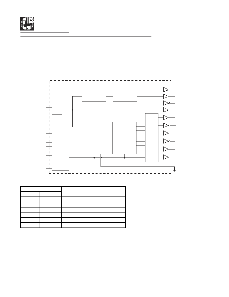
ICS954101 follows Intel CK410 Yellow Cover specification. This clock synthesizer provides a single chip solution for next
generation P4 Intel processors and Intel chipsets. ICS954101 is driven with a 14.318MHz crystal. It generates CPU outputs up
to 400MHz. It also provides a tight ppm accuracy output for Serial ATA and PCI-Express support.
General Description
Block Diagram
Power Groups
I REF
PLL2
Frequency
Dividers
Programmable
Spread
PLL1
Programmable
Frequency
Dividers
STOP
Logic
48MHz, USB
X1
X2
XTAL
SDATA
SCLK
Vtt_PWRGD#/PD
FS_A
FS_B
FS_C
ITP_EN
TEST_MODE
TEST_SEL
Control
Logic
REFOUT
CPUCLKT (2:0)
CPUCLKC (2:0)
SRCCLKT (7:0)
SRCCLKC (7:0)
PCICLK (5:0)
PCICLKF (2:0)
96MHz_DOTT_0
96MHz_DOTC_0
VDD
GND
48
51
Xtal, Ref
1,7
2,6
PCICLK outputs
21,28,34
29
SRCCLK outputs
37
38
Master clock, CPU Analog
11
13
DOT, USB, PLL_48
42
45
CPUCLK clocks
Description
Pin Number
5
Integrated
Circuit
Systems, Inc.
ICS954101
0815D--06/21/04
General I
2
C serial interface information for the ICS954101
How to Write:
∑
Controller (host) sends a start bit.
∑ Controller (host) sends the write address D2
(H)
∑ ICS clock will
acknowledge
∑ Controller (host) sends the begining byte location = N
∑ ICS clock will
acknowledge
∑ Controller (host) sends the data byte count = X
∑ ICS clock will
acknowledge
∑ Controller (host) starts sending
Byte N through
Byte N + X -1
(see Note 2)
∑ ICS clock will
acknowledge each byte one at a time
∑ Controller (host) sends a Stop bit
How to Read:
∑ Controller (host) will send start bit.
∑ Controller (host) sends the write address D2
(H)
∑ ICS clock will
acknowledge
∑ Controller (host) sends the begining byte
location = N
∑ ICS clock will
acknowledge
∑ Controller (host) will send a separate start bit.
∑ Controller (host) sends the read address D3
(H)
∑ ICS clock will
acknowledge
∑ ICS clock will send the data byte count = X
∑ ICS clock sends
Byte N + X -1
∑ ICS clock sends
Byte 0 through byte X (if X
(H)
was written to byte 8)
.
∑ Controller (host) will need to acknowledge each byte
∑ Controllor (host) will send a not acknowledge bit
∑ Controller (host) will send a stop bit
ICS (Slave/Receiver)
T
WR
ACK
ACK
ACK
ACK
ACK
P
stoP bit
X Byt
e
Index Block Write Operation
Slave Address D2
(H)
Beginning Byte = N
WRite
starT bit
Controller (Host)
Byte N + X - 1
Data Byte Count = X
Beginning Byte N
T
starT bit
WR
WRite
RT
Repeat starT
RD
ReaD
Beginning Byte N
Byte N + X - 1
N
Not acknowledge
P
stoP bit
Slave Address D3
(H)
Index Block Read Operation
Slave Address D2
(H)
Beginning Byte = N
ACK
ACK
Data Byte Count = X
ACK
ICS (Slave/Receiver)
Controller (Host)
X Byt
e
ACK
ACK