 | –≠–ª–µ–∫—Ç—Ä–æ–Ω–Ω—ã–π –∫–æ–º–ø–æ–Ω–µ–Ω—Ç: 74FCT823T | –°–∫–∞—á–∞—Ç—å:  PDF PDF  ZIP ZIP |
INDUSTRIAL TEMPERATURE RANGE
IDT74FCT823AT/CT
HIGH-PERFORMANCE CMOS BUS INTERFACE REGISTER
1
AUGUST 2000
INDUSTRIAL TEMPERATURE RANGE
The IDT logo is a registered trademark of Integrated Device Technology, Inc.
© 2000 Integrated Device Technology, Inc.
DSC-5487/1
FEATURES:
∑ A and C grades
∑ Low input and output leakage
1µA (max.)
∑ CMOS power levels
∑ True TTL input and output compatibility:
≠ V
OH
= 3.3V (typ.)
≠ V
OL
= 0.3V (typ.)
∑ High Drive outputs (-15mA I
OH
, 48mA I
OL
)
∑ Meets or exceeds JEDEC standard 18 specifications
∑ Power off disable outputs permit "live insertion"
∑ Available in the SOIC, SSOP, and QSOP packages
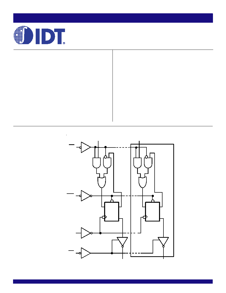
FUNCTIONAL BLOCK DIAGRAM
IDT74FCT823AT/CT
HIGH-PERFORMANCE
CMOS BUS
INTERFACE REGISTER
DESCRIPTION:
The FCT823T series is built using an advanced dual metal CMOS
technology. The FCT823T series bus interface registers are designed to
eliminate the extra packages required to buffer existing registers and
provide extra data width for wider address/data paths or buses carrying
parity. The FCT823T is a 9-bit wide buffered register with Clock Enable
(EN) and Clear (CLR) ≠ ideal for parity bus interfacing in high-performance
microprogrammed systems.
The FCT823T high-performance interface family can drive large capacitive
loads, while providing low-capacitance bus loading at both inputs and
outputs. All inputs have clamp diodes and all outputs are designed for low-
capacitance bus loading in high-impedance state.
D
CP
Q
Q
C L
D
CP
Q
Q
CL
D
0
D
N
Y
0
Y
N
EN
CLR
CP
OE
INDUSTRIAL TEMPERATURE RANGE
2
IDT74FCT823AT/CT
HIGH-PERFORMANCE CMOS BUS INTERFACE REGISTER
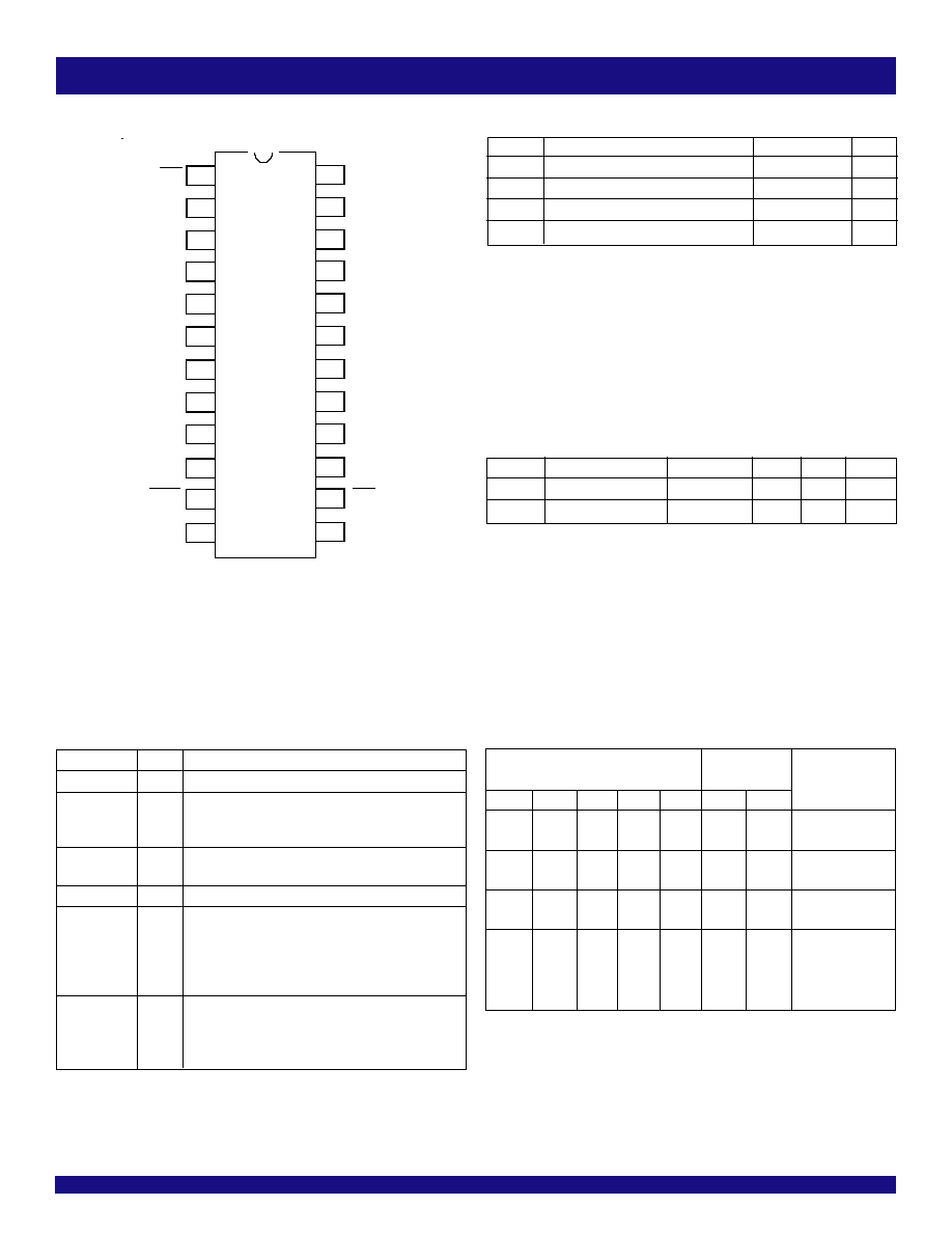
PIN CONFIGURATION
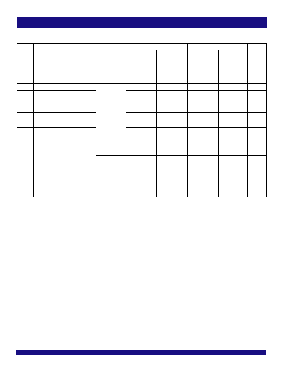
Symbol
Description
Max
Unit
V
TERM
(2)
Terminal Voltage with Respect to GND
≠0.5 to +7
V
V
TERM
(3)
Terminal Voltage with Respect to GND
≠0.5 to V
CC
+0.5
V
T
STG
Storage Temperature
≠65 to +150
∞C
I
OUT
DC Output Current
≠60 to +120
mA
ABSOLUTE MAXIMUM RATINGS
(1)
NOTES:
1. Stresses greater than those listed under ABSOLUTE MAXIMUM RATINGS may cause
permanent damage to the device. This is a stress rating only and functional operation
of the device at these or any other conditions above those indicated in the operational
sections of this specification is not implied. Exposure to absolute maximum rating
conditions for extended periods may affect reliability. No terminal voltage may exceed
Vcc by +0.5V unless otherwise noted.
2. Inputs and Vcc terminals only.
3. Output and I/O terminals only.
Symbol
Parameter
(1)
Conditions
Typ.
Max.
Unit
C
IN
Input Capacitance
V
IN
= 0V
6
10
pF
C
OUT
Output Capacitance
V
OUT
= 0V
8
12
pF
CAPACITANCE
(T
A
= +25∞C, F = 1.0MHz)
NOTE:
1. This parameter is measured at characterization but not tested.
FUNCTION TABLE
(1)
Internal/
Inputs
Outputs
OE
CLR
EN
Dx
CP
Qx
Yx
Function
H
H
L
L
L
Z
High Z
H
H
L
H
H
Z
H
L
X
X
X
L
Z
Clear
L
L
X
X
X
L
L
H
H
H
X
X
N C
Z
Hold
L
H
H
X
X
N C
N C
H
H
L
L
L
Z
Load
H
H
L
H
H
Z
L
H
L
L
L
L
L
H
L
H
H
H
NOTE:
1. H = HIGH Voltage Level
X = Don't Care
L = LOW Voltage Level
NC = No Change
= LOW-to-HIGH Transition
Z = High Impedance
2
3
1
20
19
18
15
16
9
10
D
6
D
7
D
2
D
5
D
3
D
4
D
8
23
22
24
21
17
5
6
7
4
SO24-2
SO24-7
SO24-8
8
D
0
V
CC
C P
OE
13
14
11
12
D
1
GND
CLR
Y
6
Y
7
Y
2
Y
5
Y
3
Y
4
Y
8
Y
0
Y
1
EN
SOIC/ SSOP/ QSOP
TOP VIEW
Pin Names
I/O
Description
Dx
I
D Flip-Flop Data Inputs
CLR
I
When the clear input is LOW and OE is LOW, the
Qx outputs are LOW. When the clear input is HIGH,
data can be entered into the register.
C P
I
Clock Pulse for the Register; enters data into the
register on the LOW-to-HIGH transition.
Y x
O
Register 3-State Outputs
EN
I
Clock Enable. When the clock enable is LOW, data
on the Dx output is transferred to the Qx output on the
LOW-to-HIGH transition. When the clock enable is
HIGH, the Qx outputs do not change state, regardless
of the data or clock input transitions.
OE
I
Output Control. When the OE is HIGH, the Yx
outputs are in the high-impedance state. When the
OE is LOW, the TRUE register data is present at the
Yx outputs.
PIN DESCRIPTION
INDUSTRIAL TEMPERATURE RANGE
IDT74FCT823AT/CT
HIGH-PERFORMANCE CMOS BUS INTERFACE REGISTER
3
Symbol
Parameter
Test Conditions
(1)
Min.
Typ.
(2)
Max.
Unit
V
IH
Input HIGH Level
Guaranteed Logic HIGH Level
2
--
--
V
V
IL
Input LOW Level
Guaranteed Logic LOW Level
--
--
0.8
V
I
IH
Input HIGH Current
(4)
V
CC
= Max.
V
I
= 2.7V
--
--
±1
µA
I
IL
Input LOW Current
(4)
V
CC
= Max.
V
I
= 0.5V
--
--
±1
µA
I
OZH
High Impedance Output Current
(4)
V
CC
= Max., V
I
= V
CC
(Max.)
V
I
= 2.7V
--
--
±1
µA
I
OZL
V
I
= 0.5V
--
--
±1
I
I
Input HIGH Current
(4)
V
CC
= Max., V
I
= V
CC
(Max.)
--
--
±1
µA
V
IK
Clamp Diode Voltage
V
CC
= Min., I
IN
= ≠18mA
--
≠0.7
≠1.2
V
V
H
Input Hysteresis
--
--
200
--
mV
I
CC
Quiescent Power Supply Current
V
CC
= Max.
--
0.01
1
mA
V
IN
= GND or V
CC
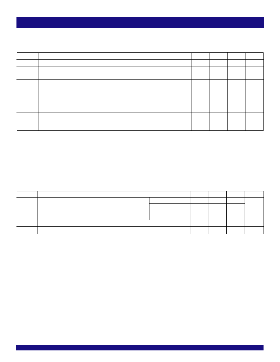
DC ELECTRICAL CHARACTERISTICS OVER OPERATING RANGE
Following Conditions Apply Unless Otherwise Specified:
Industrial: T
A
= ≠40∞C to +85∞C, V
CC
= 5.0V ±5%
NOTES:
1. For conditions shown as Min. or Max., use appropriate value specified under Electrical Characteristics for the applicable device type.
2. Typical values are at V
CC
= 5.0V, +25∞C ambient.
3. Not more than one output should be tested at one time. Duration of the test should not exceed one second.
4. The test limit for this parameter is ±5µA at T
A
= ≠55∞C.
5. This parameter is guaranteed but not tested.
Symbol
Parameter
Test Conditions
(1)
Min.
Typ.
(2)
Max.
Unit
V
OH
Output HIGH Voltage
V
CC
= Min
I
OH
= ≠8mA
2.4
3.3
--
V
V
IN
= V
IH
or V
IL
I
OH
= ≠15mA
2
3
--
V
OL
Output LOW Voltage
V
CC
= Min
I
OL
= 48mA
--
0.3
0.5
V
V
IN
= V
IH
or V
IL
I
OS
Short Circuit Current
V
CC
= Max., V
O
= GND
(3)
≠60
≠120
≠225
mA
I
OFF
Input/Output Power Off Leakage
(5)
V
CC
= 0V, V
IN
or V
O
4.5V
--
--
±1
µA
OUTPUT DRIVE CHARACTERISTICS
INDUSTRIAL TEMPERATURE RANGE
4
IDT74FCT823AT/CT
HIGH-PERFORMANCE CMOS BUS INTERFACE REGISTER
Symbol
Parameter
Test Conditions
(1)
Min.
Typ.
(2)
Max.
Unit
I
CC
Quiescent Power Supply Current
V
CC
= Max.
--
0.5
2
mA
TTL Inputs HIGH
V
IN
= 3.4V
(3)
I
CCD
Dynamic Power Supply
V
CC
= Max.
V
IN
= V
CC
--
0.15
0.25
mA/
Current
(4)
Outputs Open
V
IN
= GND
MHz
OE = EN = GND
One Input Toggling
50% Duty Cycle
I
C
Total Power Supply Current
(6)
V
CC
= Max.
V
IN
= V
CC
--
1.5
3.5
mA
Outputs Open
V
IN
= GND
f
CP
= 10MHz
50% Duty Cycle
OE = EN = GND
V
IN
= 3.4V
--
2
5.5
One Bit Toggling
V
IN
= GND
at fi = 5MHz
V
CC
= Max.
V
IN
= V
CC
--
3.8
7.3
(5)
Outputs Open
V
IN
= GND
f
CP
= 10MHz
50% Duty Cycle
OE = EN = GND
V
IN
= 3.4V
--
6
16.3
(5)
Eight Bits Toggling
V
IN
= GND
at fi = 2.5MHz
NOTES:
1. For conditions shown as Min. or Max., use appropriate value specified under Electrical Characteristics for the applicable device type.
2. Typical values are at V
CC
= 5.0V, +25∞C ambient.
3. Per TTL driven input; (V
IN
= 3.4V). All other inputs at V
CC
or GND.
4. This parameter is not directly testable, but is derived for use in Total Power Supply Calculations.
5. Values for these conditions are examples of
I
CC
formula. These limits are guaranteed but not tested.
6. I
C
= I
QUIESCENT
+ I
INPUTS
+ I
DYNAMIC
I
C
= I
CC
+
I
CC
D
H
N
T
+ I
CCD
(f
CP
/2+ f
i
N
i
)
I
CC
= Quiescent Current
I
CC
= Power Supply Current for a TTL High Input (V
IN
= 3.4V)
D
H
= Duty Cycle for TTL Inputs High
N
T
= Number of TTL Inputs at D
H
I
CCD
= Dynamic Current caused by an Input Transition Pair (HLH or LHL)
f
CP
= Clock Frequency for Register Devices (Zero for Non-Register Devices)
f
i
= Output Frequency
N
i
= Number of Outputs at f
i
All currents are in milliamps and all frequencies are in megahertz.
POWER SUPPLY CHARACTERISTICS
INDUSTRIAL TEMPERATURE RANGE
IDT74FCT823AT/CT
HIGH-PERFORMANCE CMOS BUS INTERFACE REGISTER
5
SWITCHING CHARACTERISTICS OVER OPERATING RANGE
FCT823AT
FCT823CT
Symbol
Parameter
Condition
(1)
Min
.
(2)
Max.
Min
.
(2)
Max.
Unit
t
PLH
Propagation Delay
C
L
= 50pF
1.5
10
1.5
6
ns
t
PHL
CP to
Yx (OE = LOW)
R
L
= 500
C
L
= 300pF
(4)
1.5
20
1.5
12.5
ns
R
L
= 500
t
SU
Set-up
Time HIGH or LOW
Dx
to CP
C
L
= 50pF
4
--
3
--
ns
t
H
Hold Time HIGH or LOW
Dx
to CP
R
L
= 500
2
--
1.5
--
ns
t
SU
Set-up Time HIGH or LOW EN to CP
4
--
3
--
ns
t
H
Hold Time HIGH or LOW EN to CP
2
--
0
--
ns
t
PHL
Propagation Delay, CLR to
Yx
1.5
14
1.5
8
ns
t
REM
Recovery Time CLR to CP
6
--
6
--
ns
t
W
Clock Pulse Width HIGH or LOW
7
--
6
--
ns
t
W
CLR Pulse Width LOW
6
--
6
--
ns
t
PZH
Output Enable Time OE to
Yx
C
L
= 50pF
1.5
12
1.5
7
ns
t
PZL
R
L
= 500
C
L
= 300pF
(4)
1.5
23
1.5
12.5
ns
R
L
= 500
t
PHZ
Output Disable Time OE to
Yx
C
L
= 5pF
(4)
1.5
7
1.5
6
ns
t
PLZ
R
L
= 500
C
L
= 50pF
1.5
8
1.5
6.5
ns
R
L
= 500
NOTES:
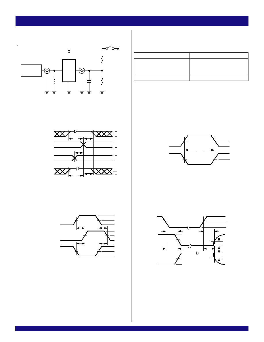
1. See test circuit and waveforms.
2. Minimum limits are guaranteed but not tested on Propagation Delays.
3. This parameter is guaranteed but not tested.
4. This condition is guaranteed but not tested.
INDUSTRIAL TEMPERATURE RANGE
6
IDT74FCT823AT/CT
HIGH-PERFORMANCE CMOS BUS INTERFACE REGISTER
Pulse
G enerator
R
T
D.U.T.
V
CC
V
IN
C
L
V
OU T
50pF
500
500
7.0V
3V
1.5V
0V
3V
1.5V
0V
3V
1.5V
0V
3V
1.5V
0V
DATA
IN PUT
TIM ING
INPUT
ASYNC HR O NOU S C ON TROL
PRES ET
C LEAR
ETC.
SYN CH RON OUS C ONTR OL
t
S U
t
H
t
RE M
t
S U
t
H
H IGH-LOW -HIG H
PULSE
LOW -H IGH -LOW
PULSE
t
W
1.5V
1.5V
SAM E PH ASE
IN PU T TR AN SITION
3V
1.5V
0V
1.5V
V
O H
t
PL H
O UTPUT
OPPOSITE PH ASE
IN PU T TR AN SITION
3V
1.5V
0V
t
P LH
t
P H L
t
P H L
V
O L
C ONTR OL
INPU T
3V
1.5V
0V
3.5V
0V
OUTPU T
N ORM A LLY
LOW
OUTPU T
N ORM A LLY
H IGH
SW ITCH
CLO SE D
SW ITC H
OPEN
V
O L
0.3V
0.3V
t
PLZ
t
PZL
t
P ZH
t
PH Z
3.5V
0V
1.5V
1.5V
EN AB LE
DISA BLE
V
O H
PRES ET
C LEAR
CLOCK ENABLE
ETC.
Octal link
Octal link
Octal link
Octal link
Octal link
TEST CIRCUITS AND WAVEFORMS
Propagation Delay
Test Circuits for All Outputs
Enable and Disable Times
Set-Up, Hold, and Release Times
Pulse Width
NOTES:
1. Diagram shown for input Control Enable-LOW and input Control Disable-HIGH.
2. Pulse Generator for All Pulses: Rate
1.0MHz; t
F
2.5ns; t
R
2.5ns.
Test
Switch
Open Drain
Disable Low
Closed
Enable Low
All Other Tests
Open
SWITCH POSITION
DEFINITIONS:
C
L
= Load capacitance: includes jig and probe capacitance.
R
T
= Termination resistance: should be equal to Z
OUT
of the Pulse Generator.
INDUSTRIAL TEMPERATURE RANGE
IDT74FCT823AT/CT
HIGH-PERFORMANCE CMOS BUS INTERFACE REGISTER
7
ORDERING INFORMATION
CORPORATE HEADQUARTERS
for SALES:
for Tech Support:
2975 Stender Way
800-345-7015 or 408-727-6116
logichelp@idt.com
Santa Clara, CA 95054
fax: 408-492-8674
(408) 654-6459
www.idt.com
XX
Tem p. R ange
XXXX
D evice Type
X
Package
SO
PY
Q
823AT
823C T
Sm all O utline IC (SO 24-2)
Shrink Sm a ll O utline Package (SO24-7)
Q uarter-size Sm all Ou tline Package (SO 24-8)
Bus Interface R egister
74
- 40∞C to +85∞C
ID T
FC T