INDUSTRIAL TEMPERATURE RANGE
IDT74LVC16652A
3.3V CMOS 16-BIT BUS REGISTERED TRANSCEIVER
1
MARCH 1999
INDUSTRIAL TEMPERATURE RANGE
The IDT logo is a registered trademark of Integrated Device Technology, Inc.
© 1999 Integrated Device Technology, Inc.
DSC-4487/2
FEATURES:
∑ Typical t
SK(o)
(Output Skew) < 250ps
∑ ESD > 2000V per MIL-STD-883, Method 3015; > 200V using
machine model (C = 200pF, R = 0)
∑ V
CC
= 3.3V ± 0.3V, Normal Range
∑ V
CC
= 2.7V to 3.6V, Extended Range
∑ CMOS power levels (0.4
µµ
µµ
µ W typ. static)
∑ All inputs, outputs, and I/O are 5V tolerant
∑ Supports hot insertion
∑ Available in SSOP, TSSOP, and TVSOP packages
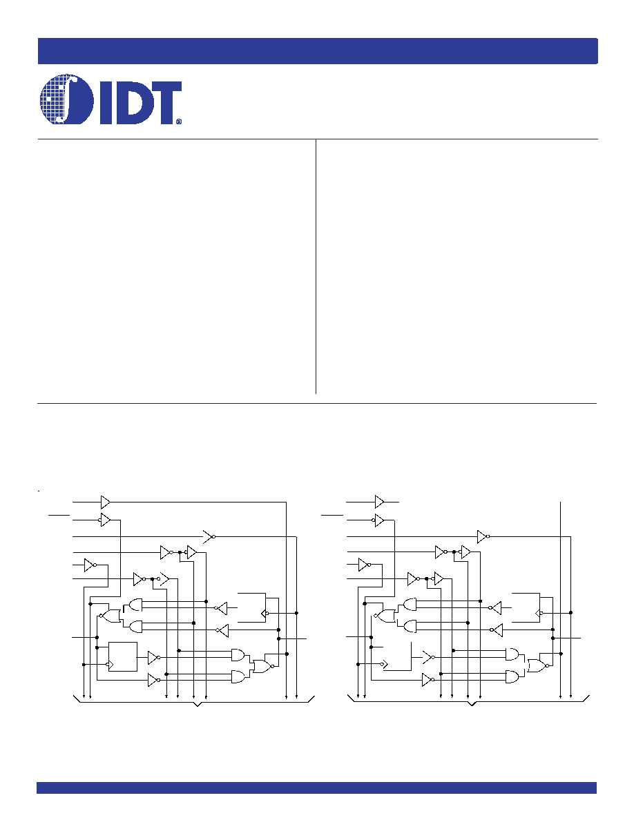
FUNCTIONAL BLOCK DIAGRAM
APPLICATIONS:
∑ 5V and 3.3V mixed voltage systems
∑ Data communication and telecommunication systems
DRIVE FEATURES:
∑ High Output Drivers: ±24mA
∑ Reduced system switching noise
IDT74LVC16652A
DESCRIPTION:
The LVC16652A 16-bit registered transceiver is built using advanced
dual metal CMOS technology. This high-speed, low power device is
organized as two independent 8-bit bus transceivers with 3-state D-type
registers. For example, the OEAB and OEBA signals control the transceiver
functions.
The SAB and the SBA control pins are provided to select either real time
or stored data transfer. The circuitry used for select control will eliminate the
typical decoding glitch that occurs in a multiplexer during the transition
between stored and real time data. A Low input level selects real-time data
and a High level selects stored data.
Data on the A or B data bus, or both, can be stored in the internal D-flip-
flops by the Low-to-High transitions at the appropriate clock pins (CLKAB
or CLKBA), regardless of the select or enable control pins. Flow-through
organization of signal pins simplifies layout. All inputs are designed with
hysteresis for improved noise margin.
The LVC16652A is ideally suited for driving high capacitance loads and
low-impedance backplanes.
All pins can be driven from either a 3.3V or 5V device. This feature allows
the use of this device as a translator in a mixed 3.3V/5V supply system.
3.3V CMOS 16-BIT BUS
REGISTERED TRANSCEIVER,
5 VOLT TOLERANT I/O
TO SEVEN OTHER CHANNELS
1
B
1
B REG
D
C
A REG
D
C
1
A
1
1
SAB
1
SBA
2
B
1
B REG
D
C
A REG
D
C
2
A
1
2
SAB
2
CLKAB
2
SBA
2
CLKBA
55
54
2
3
5
30
31
27
26
15
52
42
1
CLKAB
1
CLKBA
1
OEAB
1
OEBA
2
OEAB
2
OEBA
28
29
1
56
TO SEVEN OTHER CHANNELS

INDUSTRIAL TEMPERATURE RANGE
2
IDT74LVC16652A
3.3V CMOS 16-BIT BUS REGISTERED TRANSCEIVER
SSOP/ TSSOP/ TVSOP
TOP VIEW
PIN CONFIGURATION
Symbol
Description
Max
Unit
V
TERM
Terminal Voltage with Respect to GND
≠0.5 to +6.5
V
T
STG
Storage Temperature
≠65 to +150
∞C
I
OUT
DC Output Current
≠50 to +50
mA
I
IK
Continuous Clamp Current,
≠50
mA
I
OK
V
I
< 0 or V
O
< 0
I
CC
Continuous Current through each
±100
mA
I
SS
V
CC
or GND
ABSOLUTE MAXIMUM RATINGS
(1)
NOTE:
1. Stresses greater than those listed under ABSOLUTE MAXIMUM RATINGS may cause
permanent damage to the device. This is a stress rating only and functional operation
of the device at these or any other conditions above those indicated in the operational
sections of this specification is not implied. Exposure to absolute maximum rating
conditions for extended periods may affect reliability.
NOTE:
1. As applicable to the device type.
Symbol
Parameter
(1)
Conditions
Typ.
Max.
Unit
C
IN
Input Capacitance
V
IN
= 0V
4.5
6
pF
C
OUT
Output Capacitance
V
OUT
= 0V
6.5
8
pF
C
I/O
I/O Port Capacitance
V
IN
= 0V
6.5
8
pF
CAPACITANCE
(T
A
= +25∞C, F = 1.0MHz)
Pin Names
Description
xAx
Data Register A Inputs
Data Register B Outputs
xBx
Data Register B Inputs
Data Register A Outputs
xCLKAB, xCLKBA
Clock Pulse Inputs
xSAB, xSBA
Output Data Source Select Inputs
xOEAB, xOEBA
Output Enable Inputs
PIN DESCRIPTION
1
OEAB
1
SAB
GND
1
A
1
V
CC
GND
GND
V
CC
2
3
4
5
6
7
8
9
10
11
12
13
14
15
16
17
18
19
20
21
22
23
24
47
46
45
44
43
42
41
40
39
38
37
36
35
34
33
48
49
50
51
52
53
54
55
56
1
GND
25
26
27
28
32
31
30
29
1
CLKAB
1
A
2
1
A
3
1
A
4
1
A
5
1
A
6
1
A
7
1
A
8
2
A
1
2
A
2
2
A
3
2
A
4
2
A
5
2
A
6
2
A
7
2
A
8
2
SAB
2
CLKAB
2
OEAB
1
OEBA
1
SBA
GND
1
B
1
V
CC
GND
GND
V
CC
GND
1
CLKBA
1
B
2
1
B
3
1
B
4
1
B
5
1
B
6
1
B
8
2
B
1
2
B
2
2
B
3
2
B
4
2
B
5
2
B
6
2
B
7
2
B
8
2
SBA
2
CLKBA
2
OEBA
1
B
7
INDUSTRIAL TEMPERATURE RANGE
IDT74LVC16652A
3.3V CMOS 16-BIT BUS REGISTERED TRANSCEIVER
3
NOTES:
1. H = HIGH Voltage Level
X = Don't Care
L = LOW Voltage Level
= LOW-to-HIGH transition
2. Select Control = L: clocks can occur simultaneously.
Select Control = H: clocks can be staggered to load both registers.
3. The data output functions may be enabled or disabled by various signals at the xOEAB or xOEBA inputs. Data input functions are always enabled, i.e. data at the bus pins
will be stored on every LOW-to-HIGH transition of the clock inputs.
FUNCTION TABLE
(1,2)
Inputs
Data I/O
(3)
xOEAB
xOEBA
xCLKAB
xCLKBA
xSAB
xSBA
xAx
xBx
Operation or Function
L
H
H or L
H or L
X
X
Input
Input
Isolation
L
H
X
X
Store A and B data
X
H
H or L
X
X
Input
Unspecified
(3)
Store A, Hold B
H
H
X
(2)
X
Input
Output
Store A in both registers
L
X
H or L
X
X
Unspecified
(3)
Input
Store B, Hold A
L
L
X
X
(2)
Output
Input
Store B in both registers
L
L
X
X
X
L
Output
Input
Real time B data to A bus
L
L
X
H or L
X
H
Store B data to A bus
H
H
X
X
L
X
Input
Output
Real time A data to B bus
H
H
H or L
X
H
X
Store A data to B bus
H
L
H or L
H or L
H
H
Output
Output
Store A data to B bus and
Store B data to A bus
Symbol
Parameter
Test Conditions
Min.
Typ.
(1)
Max.
Unit
V
IH
Input HIGH Voltage Level
V
CC
= 2.3V to 2.7V
1.7
--
--
V
V
CC
= 2.7V to 3.6V
2
--
--
V
IL
Input LOW Voltage Level
V
CC
= 2.3V to 2.7V
--
--
0.7
V
V
CC
= 2.7V to 3.6V
--
--
0.8
I
IH
Input Leakage Current
V
CC
= 3.6V
V
I
= 0 to 5.5V
--
--
±5
µA
I
IL
I
OZH
High Impedance Output Current
V
CC
= 3.6V
V
O
= 0 to 5.5V
--
--
±10
µA
I
OZL
(3-State Output pins)
I
OFF
Input/Output Power Off Leakage
V
CC
= 0V, V
IN
or V
O
5.5V
--
--
±50
µA
V
IK
Clamp Diode Voltage
V
CC
= 2.3V, I
IN
= ≠18mA
--
≠0.7
≠1.2
V
V
H
Input Hysteresis
V
CC
= 3.3V
--
100
--
mV
I
CCL
Quiescent Power Supply Current
V
CC
= 3.6V
V
IN
= GND or V
CC
--
--
10
µA
I
CCH
I
CCZ
3.6
V
IN
5.5V
(2)
--
--
10
I
CC
Quiescent Power Supply Current
One input at V
CC
- 0.6V, other inputs at V
CC
or GND
--
--
500
µA
Variation
DC ELECTRICAL CHARACTERISTICS OVER OPERATING RANGE
Following Conditions Apply Unless Otherwise Specified:
Operating Condition: T
A
= ≠40∞C to +85∞C
NOTES:
1. Typical values are at V
CC
= 3.3V, +25∞C ambient.
2. This applies in the disabled state only.

INDUSTRIAL TEMPERATURE RANGE
4
IDT74LVC16652A
3.3V CMOS 16-BIT BUS REGISTERED TRANSCEIVER
BUS
A
BUS
B
xOEAB
L
xOEBA
L
xCLKAB
X
xCLKBA
X
xSAB
X
xSBA
L
BUS
A
BUS
B
xOEAB
H
xOEBA
H
xCLKAB
X
xCLKBA
X
xSAB
L
xSBA
X
BUS
A
BUS
B
xOEAB
X
L
L
xOEBA
H
X
H
xCLKAB
X
xCLKBA
X
xSAB
X
X
X
xSBA
X
X
X
BUS
A
BUS
B
xOEAB
H
xOEBA
L
xCLKAB
H or L
xCLKBA
H or L
xSAB
H
xSBA
H
REAL-TIME TRANSFER
BUS B TO A
REAL-TIME TRANSFER
BUS A TO B
STORAGE FROM
A, B, OR A AND B
TRANSFER STORED
DATA TO A AND/OR B
INDUSTRIAL TEMPERATURE RANGE
IDT74LVC16652A
3.3V CMOS 16-BIT BUS REGISTERED TRANSCEIVER
5
NOTE:
1. V
IH
and V
IL
must be within the min. or max. range shown in the DC ELECTRICAL CHARACTERISTICS OVER OPERATING RANGE table for the appropriate V
CC
range.
T
A
= ≠ 40∞C to + 85∞C.
OUTPUT DRIVE CHARACTERISTICS
Symbol
Parameter
Test Conditions
(1)
Min.
Max.
Unit
V
OH
Output HIGH Voltage
V
CC
= 2.3V to 3.6V
I
OH
= ≠ 0.1mA
V
CC
≠ 0.2
--
V
V
CC
= 2.3V
I
OH
= ≠ 6mA
2
--
V
CC
= 2.3V
I
OH
= ≠ 12mA
1.7
--
V
CC
= 2.7V
2.2
--
V
CC
= 3V
2.4
--
V
CC
= 3V
I
OH
= ≠ 24mA
2.2
--
V
OL
Output LOW Voltage
V
CC
= 2.3V to 3.6V
I
OL
= 0.1mA
--
0.2
V
V
CC
= 2.3V
I
OL
= 6mA
--
0.4
I
OL
= 12mA
--
0.7
V
CC
= 2.7V
I
OL
= 12mA
--
0.4
V
CC
= 3V
I
OL
= 24mA
--
0.55
OPERATING CHARACTERISTICS, V
CC
= 3.3V ± 0.3V, T
A
= 25∞C
Symbol
Parameter
Test Conditions
Typical
Unit
C
PD
Power Dissipation Capacitance per Transceiver Outputs enabled
C
L
= 0pF, f = 10Mhz
55
pF
C
PD
Power Dissipation Capacitance per Transceiver Outputs disabled
12