 | –≠–ª–µ–∫—Ç—Ä–æ–Ω–Ω—ã–π –∫–æ–º–ø–æ–Ω–µ–Ω—Ç: QS5805 | –°–∫–∞—á–∞—Ç—å:  PDF PDF  ZIP ZIP |

1
QS5805/A/B
GUARANTEED LOW SKEW CMOS CLOCK DRIVER/BUFFER
INDUSTRIAL TEMPERATURE RANGE
JULY 2000
1999 Integrated Device Technology, Inc.
DSC-4579/-
c
QS5805/A/B
INDUSTRIAL TEMPERATURE RANGE
GUARANTEED LOW SKEW
CMOS CLOCK
DRIVER/BUFFER
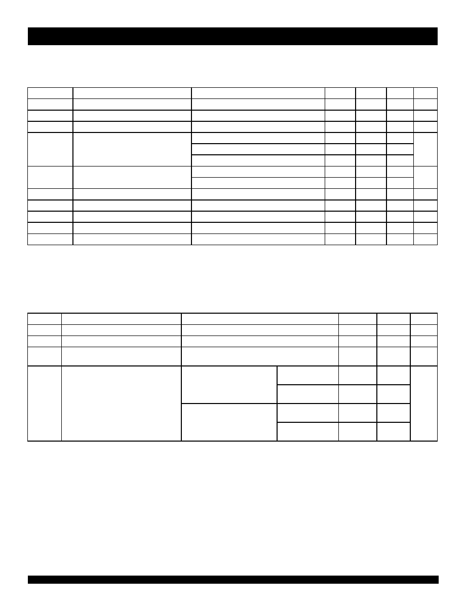
FUNCTIONAL BLOCK DIAGRAM
OE A
IN A
IN B
OA 5
OA 1
5
5
M O N
OB 5
OB 1
OE B
DESCRIPTION
The QS5805 clock buffer/driver circuits can be used for clock buffering
schemes where low skew is a key parameter. This device offers two banks
of five non-inverting outputs. The QS5805 device provides low propagation
delay buffering with on-chip skew of 0.7ns for same-transition, same-bank
signals.
The QS5805 is characterized for operation at -40∞C to +85∞C.
FEATURES:
-
10 CMOS outputs
-
Monitor output
-
Rail-to-rail output voltage swing
-
Input hysteresis for better noise margin
-
Guaranteed low skew:
∑
0.7ns output skew (same bank)
∑
0.8ns output skew (different banks)
∑
1.2ns part-to-part skew
-
Std., A, and B speed grades
-
Available in QSOP and SOIC packages
2
INDUSTRIAL TEMPERATURE RANGE
QS5805/A/B
GUARANTEED LOW SKEW CMOS CLOCK DRIVER/BUFFER
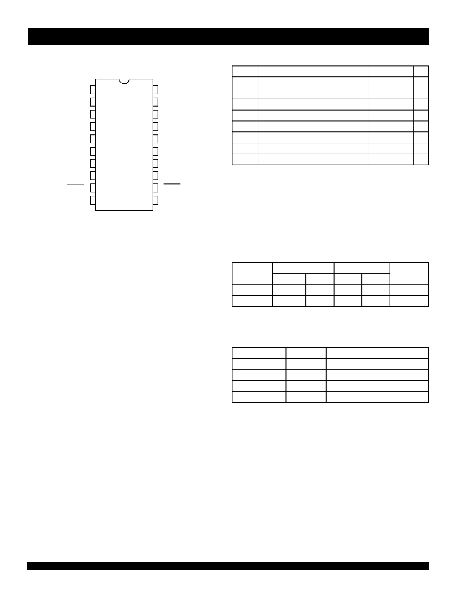
PIN CONFIGURATION
QSOP/ SOIC
TOP VIEW
1
2
3
4
5
6
7
8
9
10
20
19
18
17
16
15
14
13
12
11
O A1
O A2
O A3
G ND
A
O A4
O A5
G NDQ
O EA
INA
O B1
O B2
O B3
G ND
B
O B4
O B5
M O N
O EB
INB
V
C CA
V
C CB
SO 20-2
SO 20-8
ABSOLUTE MAXIMUM RATINGS
(1)
Symbol
Description
Max.
Unit
V
TERM(2)
Supply Voltage to Ground
≠ 0.5 to +7
V
DC Output Voltage V
OUT
≠ 0.5 to +7
V
V
TERM(3)
DC Input Voltage V
IN
≠ 0.5 to +7
V
V
AC
AC Input Voltage (pulse width
20ns)
-3
V
I
OUT
DC Output Current V
IN
< 0
-20
mA
DC Output Current Max. Sink Current/Pin
120
mA
T
STG
Storage Temperature
≠ 65 to +150
∞C
T
J
Junction Temperature
150
∞C
NOTES:
1. Stresses greater than those listed under ABSOLUTE MAXIMUM
RATINGS may cause permanent damage to the device. This is a
stress rating only and functional operation of the device at these or
any other conditions above those indicated in the operational sections
of this specification is not implied. Exposure to absolute maximum
rating conditions for extended periods may affect reliability.
2. Vcc Terminals.
3. All terminals except Vcc.
CAPACITANCE
(T
A
= +25
O
C, f = 1.0MHz, V
IN
= 0V)
QSOP
SOIC
Pins
Typ.
Max.
(1)
Typ.
Max.
(1)
Unit
C
IN
4
6
5
7
pF
C
OUT
7
9
7
9
pF
NOTE:
1. This parameter is guaranteed but not production tested.
PIN DESCRIPTION
Pin Names
I/O
Description
OEA, OEB
I
Output Enable Inputs
INA, INB
I
Clock Inputs
OAn, OBn
O
Clock Outputs
MON
O
Monitor Outputs (non-disable)
3
QS5805/A/B
GUARANTEED LOW SKEW CMOS CLOCK DRIVER/BUFFER
INDUSTRIAL TEMPERATURE RANGE
DC ELECTRICAL CHARACTERISTICS OVER OPERATING RANGE
Following Conditions Apply Unless Otherwise Specified:
Industrial: T
A
= -40∞C to +85∞C, V
CC
= 5.0V ± 10%, V
HC
= V
CC
- 0.2V, V
LC
= 0.2V
Symbol
Parameter
Test Conditions
Min.
Typ.
(1)
Max.
Unit
V
IH
Input HIGH Voltage
Guaranteed Logic HIGH for All Inputs
2
--
--
V
V
IL
Input LOW Voltage
Guaranteed Logic LOW for All Inputs
--
--
0.8
V
V
IC
Clamp Diode Voltage
(3)
Vcc = Min., I
IN
= -18mA
--
≠0.7
≠1.2
V
V
OH
Output HIGH Voltage
Vcc = Min., V
IN
= V
IH
or V
IL
, I
OH
= -300
µ
A
V
HC
Vcc
--
Vcc = Min., V
IN
= V
IH
or V
IL
, I
OH
= -15mA
3.6
4.3
--
V
Vcc = Min., V
IN
= V
IH
or V
IL
, I
OH
= -24mA
2.4
3.8
--
V
OL
Output LOW Voltage
Vcc = Min., V
IN
= V
IH
or V
IL
, I
OL
= 300
µ
A
--
GND
V
LC
V
Vcc = Min., V
IN
= V
IH
or V
IL
, I
OL
= 64mA
--
0.3
0.55
I
IN
Input Leakage Current
Vcc = Max., V
IN
= Vcc or GND
--
--
±1
µ
A
I
OZ
Output Leakage Current
Vcc = Max., V
OUT
= Vcc or GND
--
--
±1
µ
A
I
OFF
Input Power Off Leakage
Vcc = 0V, V
IN
= Vcc or GND
--
--
±1
µ
A
I
OS
Short Circuit Current
(2,3)
Vcc = Max., V
OUT
= GND
≠
60
--
--
mA
V
T
Input Hysteresis
V
TLH
- V
THL
for All Inputs
--
0.2
--
V
NOTES:
1. Typical values are at V
CC
= 5.0V, T
A
= 25∞C.
2. Not more than one output should be used to test this high power condition. Duration is less than one second.
3. Guaranteed by design but not tested.
POWER SUPPLY CHARACTERISTICS
Symbol
Parameter
Test Conditions
(1)
Typ.
(3)
Max.
Unit
I
CC
Quiescent Power Supply Current
V
CC
= Max., V
IN
= GND or Vcc
0.005
0.5
mA
I
CC
Supply Current per Input HIGH
V
CC
= Max., V
IN
= 3.4V
0.5
2.5
mA
I
CCD
Dynamic Power Supply Current per Output
(2)
V
CC
= Max.,
OEA = OEB = GND
Outputs Enabled, 50% duty cycle
0.1
0.2
mA/MHz
I
C
Total Supply Current Examples
(2,4)
V
CC
= Max.,
OEA = OEB = GND
V
IN
= GND or Vcc
8.5
15.5
50% duty cycle, f
I
= 10MHz
Five outputs toggling
V
IN
= GND or 3.4V
9
16.8
mA
V
CC
= Max.,
OEA = OEB = GND
V
IN
= GND or Vcc
5
8.8
50% duty cycle, f
I
= 2.5MHz
All outputs toggling
V
IN
= GND or 3.4V
6
11.3
NOTES:
1. For conditions shown as Min. or Max., use the appropriate values specified under DC Electrical Characteristics.
2. Guaranteed by design but not tested. C
L
= 0pF.
3. Typical values are for reference only. Conditions are V
CC
= 5.0V, T
A
= 25∞C.
4. I
C
= I
CC
+ (
I
CC
)(D
H
)(N
T
) + I
CCD
(f
O
)(N
O
)
where:
D
H
= Input Duty Cycle
N
T
= Number of TTL HIGH inputs at D
H
f
O
= Output Frequency
N
O
= Number of outputs at f
O

4
INDUSTRIAL TEMPERATURE RANGE
QS5805/A/B
GUARANTEED LOW SKEW CMOS CLOCK DRIVER/BUFFER
SKEW CHARACTERISTICS OVER OPERATING RANGE
T
A
= -40∞C to +85∞C, V
CC
= 5.0V ± 10%
C
LOAD
= 50pF, R
LOAD
= 500
unless otherwise noted.
QS5805
QS5805A
QS5805B
Symbol
Parameter
(1)
Min.
Max.
Min.
Max.
Min.
Max.
Unit
t
SK(01)
Skew between all outputs, same transition, same bank
--
0.7
--
0.7
--
0.7
ns
t
SK(02)
Skew between outputs of all banks, same transition
--
0.8
--
0.8
--
0.8
ns
t
SK(P)
Pulse Skew; skew between opposite transitions of the same
output (t
PHL
- t
PLH
)
--
1
--
1
--
1
ns
t
SK(T)
Part-to-part skew
(2)
--
1.5
--
1.5
--
1.2
ns
NOTES:
1. Skew parameters are guaranteed across temperature range, but not tested. Skew parameters are measured at 0.5Vcc.
2. t
SK(T)
only applies to devices of the same transition, part type, temperature, power supply voltage, loading, package, and speed grade.
SWITCHING CHARACTERISTICS OVER OPERATING RANGE
T
A
= -40∞C to +85∞C, V
CC
= 5.0V ± 10%
C
LOAD
= 50pF, R
LOAD
= 500
unless otherwise noted.
QS5805
QS5805A
QS5805B
Symbol
Parameter
(1)
Min.
Max.
Min.
Max.
Min.
Max.
Unit
t
PLH
t
PHL
Propagation Delay
(2)
INA to OAn, INB to OBn
1.5
5.6
1.5
5.3
1.5
5
ns
t
PZL
t
PZH
Output Enable Time
1.5
8
1.5
8
1.5
7
ns
t
PLZ
t
PHZ
Output Disable Time
1.5
7
1.5
7
1.5
6
ns
t
R
Output Rise Time
0.8V to 2V
(3)
--
1.5
--
1.5
--
1.5
ns
0.2Vcc to 0.8Vcc
--
3
--
3
--
3
ns
t
F
Output Fall Time
0.8V to 2V
(3)
--
1.5
--
1.5
--
1.5
ns
0.2Vcc to 0.8Vcc
--
3
--
3
--
3
ns
NOTES:
1. Minimums guaranteed but not production tested. Timing parameters are measured at 0.5Vcc.
2. The propagation delay other range indicated by Min. and Max. specifications results from process and environmental variables. These propagation
delays do not imply limit skew.
3. This parameter is guaranteed but not production tested.

5
QS5805/A/B
GUARANTEED LOW SKEW CMOS CLOCK DRIVER/BUFFER
INDUSTRIAL TEMPERATURE RANGE
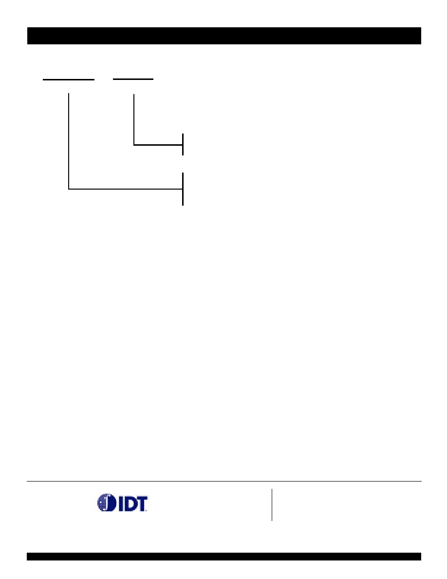
Pulse
Generator
500
500
V
CC
V
OUT
V
IN
DUT
50
50pF
7.0 V
Parameter
Tested
Switch
Position
All Others
Closed
Open
t
PLZ
, t
PZL
CONTROL
INPUT
ENABLE
DISABLE
3V
1.5V
0V
3V
0V
1.5V
1.5V
OUTPUT
NORMALLY
LOW
SWITCH
CLOSED
0.3V
0.3V
INPUT
OUPUT 1
3V
1.5V
0V
OUPUT 2
INPUT
OUPUT
3V
1.5V
0V
0.5Vcc
2.0V
0.8V
INPUT
PART 1 OUTPUT
3V
1.5V
0V
PART 2 OUTPUT
INPUT
OUPUT A
t
PLHA
3V
1.5V
0V
OUPUT B
INPUT
OUPUT
t
PLH
t
PHL
3V
1.5V
0V
V
O H
V
OL
t
SK(p)
= t
PHL
- t
PLH
t
SK(02)
= t
PLHB
- t
PLHA
or t
PHLB
- t
PHLA
Pulse generator for all pulses: f
1.0MHz; t
F
2.5ns; t
R
2.5ns
V
O H
V
OL
V
O H
V
OL
t
PHLA
t
SK(02)
t
SK(02)
t
PLHB
t
PHLB
V
O H
V
OL
V
O H
V
OL
t
SK(01)
t
SK(01)
t
SK(01)
= t
PLH2
- t
PLH1
or t
PHL2
- t
PHL1
t
PLH1
t
PHL1
t
PLH2
t
PHL2
V
O H
V
OL
V
O H
V
OL
t
PLH
t
PHL
t
R
t
F
OUTPUT
NORMALLY
HIGH
t
PZL
t
PLZ
t
PHZ
t
PZH
SWITCH
OPEN
t
PLH1
t
PHL1
t
SK(t)
t
SK(t)
t
PLH2
t
PHL2
t
SK(t)
= t
PLH2
- t
PLH1
or t
PHL2
- t
PHL1
V
O H
V
OL
V
OL
V
O H
0.5Vcc
0.5Vcc
0.5Vcc
0.5Vcc
0.5Vcc
0.5Vcc
0.5Vcc
TEST CIRCUITS AND WAVEFORMS
PROPAGATION DELAY
PULSE SKEW -- t
SK(P)
OUTPUT SKEW (SAME BANK) -- t
SK(O1)
OUPUT SKEW (DIFFERENT BANKS) -- t
SK(O2)
ENABLE AND DISABLE TIMES
PART-TO-PART SKEW -- t
SK(T)
6
INDUSTRIAL TEMPERATURE RANGE
QS5805/A/B
GUARANTEED LOW SKEW CMOS CLOCK DRIVER/BUFFER
ORDERING INFORMATION
CORPORATE HEADQUARTERS
for SALES:
2975 Stender Way
800-345-7015 or 408-727-6116
Santa Clara, CA 95054
fax: 408-492-8674
www.idt.com*
*To search for sales office near you, please click the sales button found on our home page or dial the 800# above and press 2.
The IDT logo, QuickSwitch, and SynchroSwitch are registered trademarks of Integrated Device Technology, Inc.
XXXX
Device Type
XX
Package
Q
SO
5805
5805A
5805B
Quarter Size Small Outline Pacakge (SO20-8)
Small Outline IC (SO20-2)
Guaranteed Low Skew CMOS Clock Driver/Buffer
QS