 | –≠–ª–µ–∫—Ç—Ä–æ–Ω–Ω—ã–π –∫–æ–º–ø–æ–Ω–µ–Ω—Ç: QS5925 | –°–∫–∞—á–∞—Ç—å:  PDF PDF  ZIP ZIP |

1
QS5925
PROGRAMMABLE FREQUENCY GENERATOR
INDUSTRIAL TEMPERATURE RANGE
MARCH 2000
1999 Integrated Device Technology, Inc.
DSC-5776/-
c
QS5925
INDUSTRIAL TEMPERATURE RANGE
PROGRAMMABLE
FREQUENCY GENERATOR
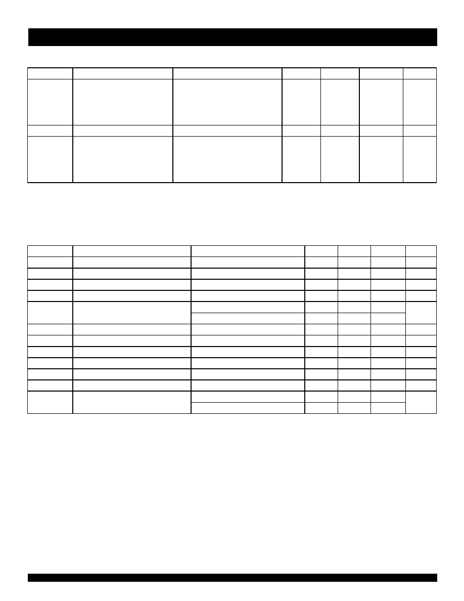
FUNCTIONAL BLOCK DIAGRAM
FEATURES
∑
4 programmable frequency outputs
∑
Optional crystal input, internal capacitors
∑
Balanced Drive Outputs ±12mA
∑
PLL disable mode for low frequency testing
∑
Tri-state output enable (
OE)
∑
PHY/MAC networking applications
∑
Industrial ≠40 to 85∞C operation
∑
Input frequencies up to 100MHz
∑
Output frequencies up to 160MHz
∑
5V tolerant inputs
∑
Low output skew/jitter
∑
External feedback, internal loop filter
∑
3V to 3.6V supply voltage
∑
Available in 16-pin QSOP package
DESCRIPTION
The QS5925 is a high-performance, low skew, low jitter phase-locked
loop (PLL) clock driver. It provides precise phase and frequency alignment
of its clock outputs to an externally applied clock input or internal crystal
oscillator. The QS5925 has been specially designed to interface with
Gigabit Ethernet and Fast Ethernet applications by providing a 125MHz
clock from 25MHz input. It can also be programmed to provide output
frequencies ranging from 3.125MHz to 160MHz with input frequencies
ranging from 3.125MHz to 100MHz. The QS5925 includes an internal RC
filter that provides excellent jitter characteristics and eliminates the need for
external components. When using the optional crystal input, the X
2
pin must
be connected to the CLK pin. The on-chip crystal oscillator includes the
feedback resistor and crystal capacitors (nominal load capacitance is
15pF), and requires a fundamental mode crystal with a maximum equiva-
lent series resistance of 50
.
PH A S E
D ETE C TO R
F B
C LKIN
X
1
X
2
O PTIO N A L
C R Y ST AL
XT A L
O SC
LO O P
FIL TER
VC O
Q /N
Q
0
Q
1
Q
2
0
1
FR EQ U EN C Y
D IVID ER
1/N
SE LE C T
M O D E
S
0
S
1
O E

2
INDUSTRIAL TEMPERATURE RANGE
QS5925
PROGRAMMABLE FREQUENCY GENERATOR
1
2
3
4
5
6
7
8
16
15
14
13
12
11
10
9
S
1
S
0
G NDQ
V
DD Q
X
1
X
2
CLKIN
FB
G NDN
Q
2
Q
1
Q
0
Q /N
G NDN
O E
V
D DN
SO 16-7
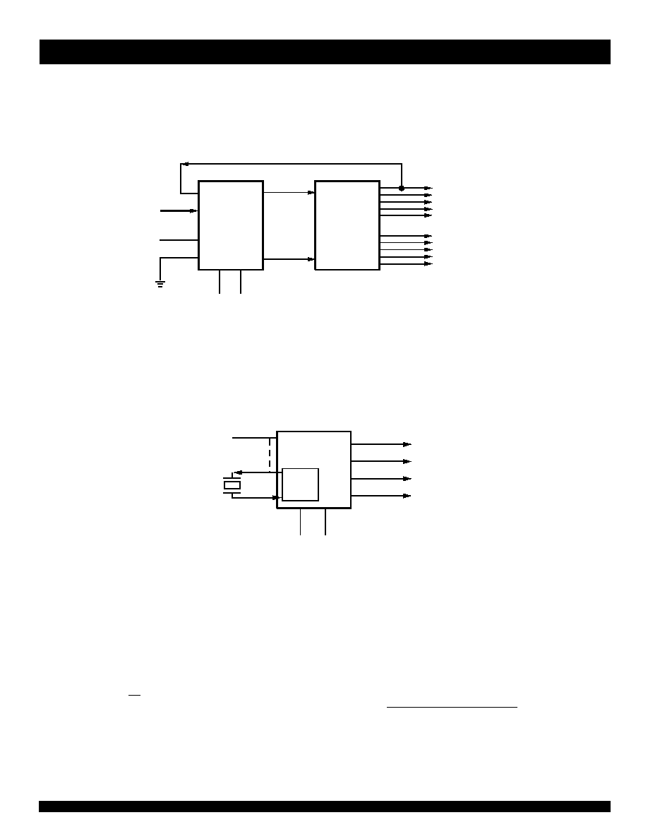
PIN CONFIGURATION
QSOP
TOP VIEW
Pin Names
QTY
I/O
Description
CLKIN
1
I
Input clock
X
1
(1)
1
I
Crystal oscillator input
X
2
(1)
1
O
Crystal oscillator output
FB
1
I
PLL feedback input which can be
connected to any Q output pin. PLL locks
onto +ve edge of FB signal.
S x
2
I
Mode/Frequency select inputs (three-level)
Q x
3
O
Clock outputs
Q/N
1
O
Programmable divide-by-N clock output
OE
1
I
Tri-state output enable. When asserted
HIGH, clock outputs are high impedance.
V
DDN
1
I
Power supply for output buffers
GNDN
2
I
Ground supply for output buffers
V
DDQ
1
I
Power supply for PLL
GNDQ
1
I
Ground supply for PLL
PIN DESCRIPTION
NOTE:
1. For best accuracy, use parallel resonant crystal specified for a load
capacitance of 15pF.
Output Used for
Allowable CLK Range (MHz)
(1)
Output Frequency Relationships
Feedback
Minimum
Maximum
Q/N
Qx
Q/N
25/N
160/N
CLK
CLK x N
Q x
25
100
CLK/N
CLK
FUNCTION TABLE
NOTE:
1. Operation in the specified CLK frequency range guarantees that the VCO will operate in the optimal range of 25MHz to 160MHz. Operation with
CLK outside specified frequency ranges may result in invalid or out-of-lock outputs.
ABSOLUTE MAXIMUM RATINGS
(1)
Symbol
Description
Max.
Unit
V
TERM
Supply Voltage to Ground
≠ 0.5 to +7
V
DC Output Voltage V
OUT
≠ 0.5 to Vcc
+0.5
V
DC Input Voltage V
IN
≠ 0.5 to +7
V
T
A
= 85
∞
C
Maximum Power Dissipation
.55
W
T
STG
Storage Temperature
≠ 65 to +150
∞C
NOTE:
1. Stresses greater than those listed under ABSOLUTE MAXIMUM
RATINGS may cause permanent damage to the device. This is a
stress rating only and functional operation of the device at these or
any other conditions above those indicated in the operational sections
of this specification is not implied. Exposure to absolute maximum
rating conditions for extended periods may affect reliability.

3
QS5925
PROGRAMMABLE FREQUENCY GENERATOR
INDUSTRIAL TEMPERATURE RANGE
DIVIDE SELECTION TABLE
(1)
NOTES:
1. H = HIGH
M = MEDIUM
L = LOW
2. Factory test mode: operation not specified.
3. Ethernet mode (use a 25MHz input frequency and Q/N as feedback).
4. Test mode for low frequency testing. In this mode, CLK bypasses the VCO (VCO powered down). Frequency must be > 1MHz due to dynamic
circuits in the frequency dividers.
S1
S0
Divide-by-N Value
Mode
L
L
FACTORY TEST
(2)
L
M
2
PLL
L
H
3
PLL
M
L
4
PLL
M
M
5
(3)
PLL
M
H
6
PLL
H
L
7
PLL
H
M
8
PLL
H
H
16
TEST
(4)
DC ELECTRICAL CHARACTERISTICS OVER OPERATING RANGE
Following Conditions Apply Unless Otherwise Specified:
Industrial: T
A
= -40∞C to +85∞C, V
CC
= 3.3V ± 0.3V
Symbol
Parameter
Test Conditions
Min.
Typ.
Max.
Unit
V
IH
Input HIGH Voltage
CLKIN, FB and
OE
2
--
--
V
V
IHH (1)
Sx
V
DD
- 0.6
--
--
V
IL
Input LOW Voltage
CLKIN, FB and
OE
--
--
0.8
V
V
ILL (1)
Sx
--
--
0.6
V
IMM (1)
Input MID Voltage
Sx
V
DD
/2 - 0.3
--
V
DD
/2 + 0.3
V
I
IH
Input HIGH Current
V
IN
= V
DD
; CLKIN, FB and
OE
- 5
0.07
5
µ
A
I
IHH
V
IN
= V
DD
; Sx
--
50
150
I
IL
Input LOW Current
V
IN
= 0V; CLKIN, FB and
OE
- 5
--
5
µ
A
I
ILL
V
IN
= 0V; Sx
- 150
- 50
--
I
IMM
Input MID Current
V
IN
= V
DD
/2; Sx
- 50
0
50
µ
A
V
OH
Output HIGH Voltage
V
DD
= 3V, I
OH
= -12mA
2.4
2.8
--
V
V
DD
= 3V, I
OH
= -100
µ
A
2.8
--
--
V
OL
Output LOW Voltage
V
DD
= 3V, I
OL
= 12mA
--
0.15
0.55
V
V
DD
= 3V, I
OL
= 100
µ
A
--
--
0.2
NOTE:
1. These inputs are normally wired to Vcc, GND, or unconnected. If the inputs are switched in real time, the function and timing of the outputs may
glitch, and the PLL may require an additional lock time before all datasheet limits are achieved.
Symbol
Parameter
Min
Typ
Max
Unit
V
DD
Power Supply Voltage
3
3.3
3.6
V
T
A
Operating Temperature
≠40
25
85
∞ C
C
L
Output Load Capacitance
--
--
15
pF
C
IN
Input Capacitance, CLKIN, FB,
OE, F = 1MHz, V
IN
= 0V, T
A
= 25∞C
--
5
7
pF
OPERATING CONDITIONS
4
INDUSTRIAL TEMPERATURE RANGE
QS5925
PROGRAMMABLE FREQUENCY GENERATOR
POWER SUPPLY CHARACTERISTICS
Symbol
Parameter
Test Conditions
(1)
Min.
Typ.
Max
Unit
I
DDQ
Quiescent Supply Current
V
DD
= Max.
CLK = FB = X
1
= GND
Sx = H
OE = H
All outputs unloaded
--
0.7
2
mA
I
DD
Supply Current per Input
V
DD
= Max., V
IN
= 3V
--
1
30
µ
A
I
DD
Dynamic Supply Current
V
DD
= 3.6V
S
0
= MID; S
1
= GND
OE = GND
F
OUT
= 60MHz
All outputs unloaded
--
77
130
mA
NOTE:
1. For conditions shown as Min. or Max., use the appropriate values specified under DC Electrical Characteristics.
AC ELECTRICAL CHARACTERISTICS OVER OPERATING RANGE
Following Conditions Apply Unless Otherwise Specified:
Industrial: T
A
= -40∞C to +85∞C, V
CC
= 3.3V ± 0.3V
Symbol
Parameter
Test Conditions
Min.
Typ.
Max.
Unit
t
R
Rise Time
(1)
0.8V to 2V
--
0.7
1.5
ns
t
F
Fall Time
(1)
2V to 0.8V
--
0.7
1.5
ns
d
T
Duty Cycle
(1)
V
T
= V
DD
/2
45
50
55
%
t
PD
CLKIN to FB Propagation Delay
(1)
V
T
= V
DD
/2
- 1.6
- 0.95
- 0.5
ns
t
SK
Skew (output - output)
(1)
V
T
= V
DD
/2; Qx
--
--
300
ps
V
T
= V
DD
/2; Q/N - Qx
--
--
600
t
J
Cycle - Cycle Jitter
(1)
For N = 2 at 125MHz output (Qx)
--
--
200
ps
d
T_INPUT
CLKIN Duty Cycle
(1)
V
T
= 1.5V
25
--
75
%
t
R_INPUT
CLKIN Rise Time
(1)
0.8V to 2V
--
--
2
ns
t
F_INPUT
CLKIN Fall Time
(1)
0.8V to 2V
--
--
2
ns
f
OSC
Oscillator Frequency
--
--
--
30
MHz
f
OUT
Output Frequency
--
25
--
160
MHz
f
IN
Input Frequency
Qx used for feedback
25
--
100
MHz
Q/N used for feedback
25/N
--
160/N
NOTE:
1. This parameter is guaranteed by design but not tested.

5
QS5925
PROGRAMMABLE FREQUENCY GENERATOR
INDUSTRIAL TEMPERATURE RANGE
TEST LOADS AND WAVEFORMS
HOW TO USE THE QS5925
The QS5925 is a general-purpose phase-locked loop (PLL) that can be
used as a zero delay buffer or a clock multiplier. It generates three outputs
at the VCO frequency and one output at the VCO frequency divided by n,
where n is determined by the Mode/Frequency Select input pins S
0
and
S
1
. The PLL will adjust the VCO frequency (within the limits of the Function
Table) to ensure that the input frequency equals the frequency of which-
ever output is connected to FB.
The QS5925 can accept two types of input signal. The first is a reference
clock generated by another device on the board which needs to be
reproduced with a minimal delay between the incoming clock and output.
The second is an external crystal. When used in the first mode, the crystal
input (X
1
) should be tied to ground and the crystal output (X
2
) should be
left unconnected. Figure 2 depicts one of the applications:
By connecting Q
0
to FB, the phase detector of the QS5925 will adjust the
output frequency of the VCO to the incoming clock in such a fashion that the
two inputs (FB and CLKIN) will have nearly zero phase and frequency
difference. In addition, one copy of the clock can be divided from 2 to 8 in
increments of one. The divide will depend on the S
0
and S
1
selection (see
Divide Selection Table on page 3). The S
0
and S
1
pins are three level inputs
that allow a total of seven different modes of division. They can be connected
HIGH, LOW or left unconnected to provide a MID level (an internal resistor
network will bias the signal level to 0.5V
DD
). Another way to use the QS5925
is to connect Q/N to FB (see Figure 3).
15pF
150
OUTPUT
V
CC
150
2V
V
T H
= V
C C
/2
0V
1ns
3V
1ns
2V
V
T H
= V
C C
/2
0V
t
R
t
F
V
C C
0.8
0.8
AC Test Load
Input Test Waveform
Output Waveform
Q S5 925
FB
CLKIN
X
2
X
1
S
0
S
1
Q
0
Q
1
Q
2
Q /N
Figure 2
F B
CLKIN
X
2
X
1
S
0
S
1
Q /N
Q
0
Q
1
Q
2
Q S5925
Figure 3
FIGURE 1
6
INDUSTRIAL TEMPERATURE RANGE
QS5925
PROGRAMMABLE FREQUENCY GENERATOR
Connected in this fashion, the QS5925 not only becomes a zero delay
buffer, but also a clock multiplier. With proper selection of S
0
and S
1
, the
Q
0
≠Q
2
outputs will generate two, three, up to eight times the input clock
frequency. When used in this mode, you must make sure that the input and
output frequency specifications are not violated (refer to Function Table).
There are some applications where higher fan-out is required. These kinds
of applications could be addressed by using the QS5925 in conjunction with
a clock buffer such as the QS53805 . Figure 4 shows how higher fan-out
with different clock rates can be generated.
By connecting one of the QS53805 outputs to the FB input of the QS5925,
the propagation delay from CLKIN to the output of the QS53805 will be
nearly zero.
The second way to drive the input of the QS5925 is via an external
crystal. When connecting an external crystal to pins 5 and 6, the X
2
pin must
be shorted to the CLKIN (pin 7) as shown in Figure 5. For best accuracy,
a parallel resonant crystal with a crystal load capacitance rating of 15pF
should be used. To reduce the parasitic between the external crystal and
the QS5925 , it is recommended to connect the crystal as close as possible
to the X
1
and X
2
pins.
One of the questions often asked is what is the accuracy of our clock
generators? In applications where clock synthesizers are used, the terms
frequency accuracy and frequency error are used interchangeably.
Here, frequency accuracy (or error) is based on two factors. One is the
input frequency and the other is the multiplication factor. Clock multipliers
(or synthesizers) are governed by the equation:
Output Frequency = (M)* Input Frequency
N
where "M" is the feedback divide and "N" is the reference divide. If the
ratio of M/N is not an integer, then the output frequency will not be an exact
multiple of the input. On the other hand, if the ratio were a whole number,
the output clock would be an exact multiple of the input. In the case of
QS5925, since the reference divide ("N") is "1", the equation is a strong
function of the feedback divide ("M"). In addition, since the feedback is an
integer, the output frequency error (or accuracy) is merely a function of how
accurate the input is. For instance, QS5925 could accept two forms of input,
one from a crystal oscillator (see Figure 3) and the other from a crystal (see
Figure 5). By using a 20MHz clock with a multiplication factor of 5 (with an
accuracy of ±30 parts per million), one can easily have three copies of
100MHz of clock with ±30PPM of accuracy. Frequency accuracy is
defined by the following equation:
Accuracy = (Measured Freq. ≠ Nominal Freq.)
Nominal Frequency
where measured frequency is the average frequency over certain
number of cycles (typically 10,000) and the nominal frequency is the
desired frequency.
Q S5 380 5
F B
C LKIN
X
2
X
1
S
0
S
1
Q X
Q /N
IN A
IN B
5 C O PIES O F Q /N
5 C O PIES O F Q
Q S5925
Figure 4
CLKIN
X
2
X
1
S
0
S
1
Q
0
Q
1
Q
2
Q /N
XTAL
O SC
QS5925
Figure 5
7
QS5925
PROGRAMMABLE FREQUENCY GENERATOR
INDUSTRIAL TEMPERATURE RANGE
ORDERING INFORMATION
CORPORATE HEADQUARTERS
for SALES:
2975 Stender Way
800-345-7015 or 408-727-6116
Santa Clara, CA 95054
fax: 408-492-8674
www.idt.com*
*To search for sales office near you, please click the sales button found on our home page or dial the 800# above and press 2.
The IDT logo, QuickSwitch, and SynchroSwitch are registered trademarks of Integrated Device Technology, Inc.
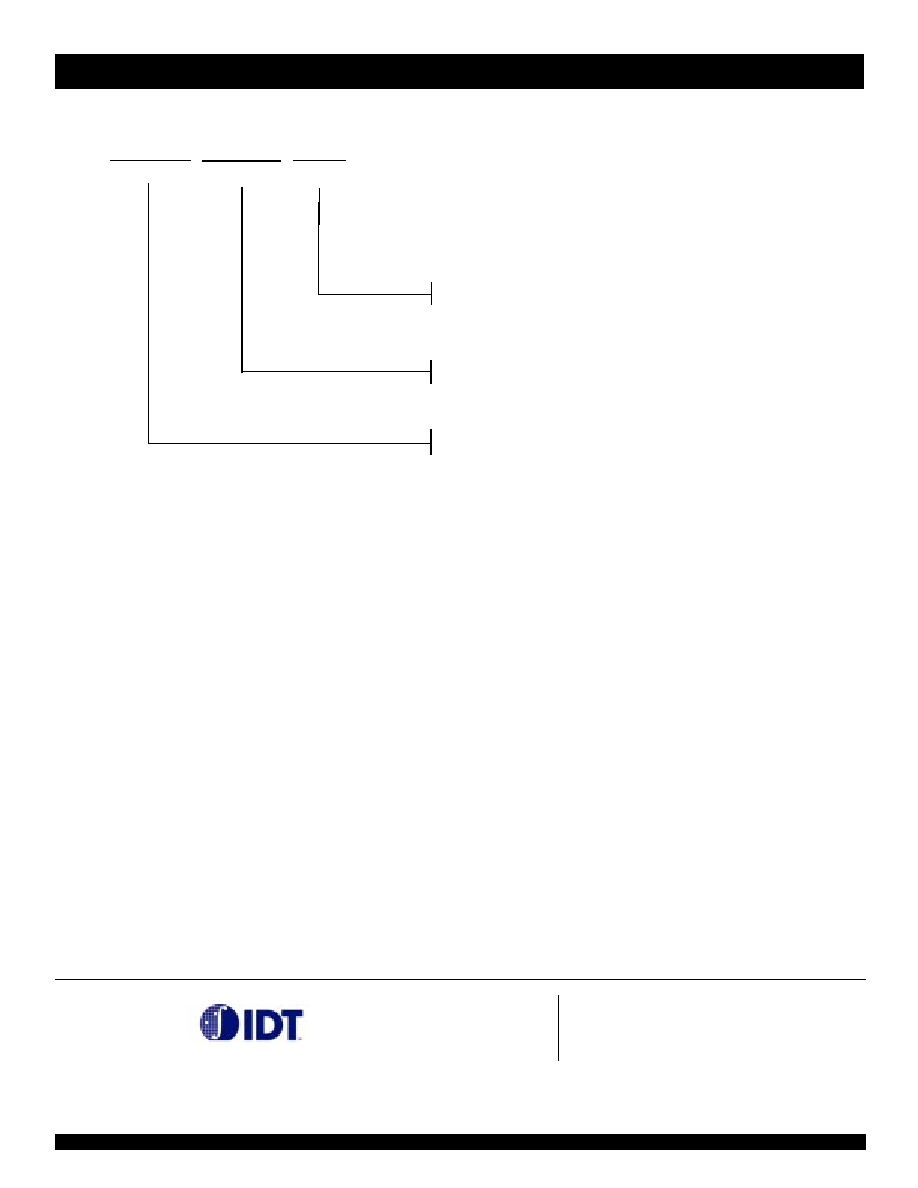
IDTQS
XXXX
X
Package
Device Type
Blank
Industrial (-40∞C to +85∞C)
Quarter Size Outline Package (150 mil.) (SO16-7)
Q
5925
Programmable Frequency Generator
X
Process