The IMP16C554 is a universal asynchronous receiver and
transmitter with 16 byte transmit and receive FIFO. A
programmable baud rate generator is provided to select
transmit and receive clock rates from 50Hz to 1.5MHz.
The IMP16C554 is an improved version of the IMP16C550
UART with higher operating speed and lower access time.
The IMP16C554 on board status registers provides the
error conditions, type and status of the transfer operation
being performed. Included is complete MODEM control
capability, and a processor interrupt system that may be
software tailored to the user's requirements. The
IMP16C554 provides internal loop-back capability for on
board diagnostic testing.
The IMP16C554 is fabricated in an advanced 1.2u CMOS
process to achieve low drain power and high speed
16 byte receive FIFO with error flags
Modem control signal (CTS*, RTS*, DSR*, DTR*,
RI* ,CD*)
Programmable character lengths(5,6,7,8)
Even, odd, or no parity bit generation and detection
Status report register
Independent transmit and receive control
TLL compatible inputs. outputs
Software compatible with Ei8250, 1Ei16C550
460.8kHz transmit/receive operation with 7.372
MHz crystal or external clock source
1
408-432-9100/www.impweb.com © 2002 IMP, Inc.
IMP16C554
IMP16C554
Data Communications
10
11
12
13
14
15
16
17
18
19
20
21
22
23
24
25
26
DSRA∑
CTSA∑
DTRA∑
VCC
RTSA∑
INTA
CSA∑
TXA
IOW∑
TXB
CSB∑
INTB
RTSB∑
GND
DTRB
CTSD∑
DSRB∑
DSRA∑
CTSA∑
DTRA∑
VCC
RTSA∑
INTA
CSA∑
TXA
IOW∑
TXB
CSB∑
INTB
RTSB∑
GND
DTRB
CTSD∑
DSRD∑
CTSD∑
DTRD∑
GND
RTSD∑
INTD
CSD∑
TXD
IOR∑
TXC
CSC∑
INTC
RTSC∑
VCC
DTRC∑
CTSC∑
DSRC∑
DSRD∑
CTSD∑
DTRD∑
GND
RTSD∑
INTD
CSD∑
TXD
IOR∑
TXC
CSC∑
INTC
RTSC∑
VCC
DTRC∑
CTSC∑
CDB∑
RIB∑
RXB∑
VCC
NC
A2
A1
A0
XT
AL1
XT
AL2
ERSET
RXRDY∑
TXRD∑
GND
RXC
RIC∑
CDC∑
DSBS∑
CDS∑
RIB∑
RXB∑
VCC
A2
A1
A0
XT
AL1
XT
AL2
RESET
GND
RXC
RIC∑
CDC∑
DSRC∑
CDA∑
RIA∑
RXA
GND
D7
D6
D5
D4
D3
D2
D1
D0
INTSEL
VCC
RXD
RID∑
CDO∑
CDA∑
RIA∑
RXA
GND
D7
D6
D5
D4
D3
D2
D1
D0
VCC
RXD
RID∑
COD∑
27
28
29
30
31
32
33
34
35
36
37
38
39
40
41
42
43
9
8
7
6
5
4
3
2
1
68
67
66
65
64
63
62
61
16C554
60
59
58
57
56
55
54
53
52
51
50
49
48
47
46
45
44
1
2
3
4
5
6
7
8
9
10
11
12
13
14
15
16
17
18
19
20
21
22
23
24
25
26
27
28
29
30
31
32
64
63
62
61
60
59
58
57
56
55
54
53
52
51
50
49
16C554
48
47
46
45
44
43
42
41
40
39
38
37
36
35
34
33
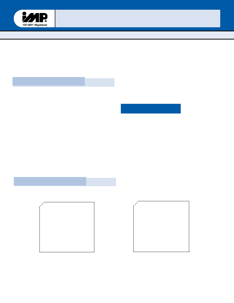
64-PIN QFP
68-PIN PLCC
IMP
IMP
requirements.
Description
Key Features
Pin Configuration
Quad Universal Asynchronous
Receiver/Transmitter (UART)
with FIFO's

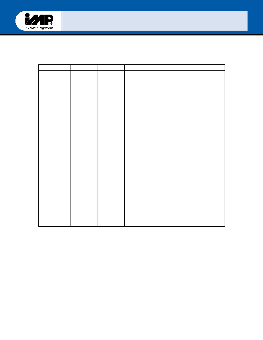
SYMBOL DESCRIPTION
symbol
pin
Signal Type Pin Description
D0-D7
RX A-B
RX C-D
TX A-B
TX C-D
CS*A-B
CS*C-D
XTAL1
XTAL2
LOW*
GND
GND
IOR*
5-66
7.29
41.63
17.19
51.53
16.20
50.54
35
36
18
6.23
40.57
52
I/O
I
O
I
I
O
I
O
I
Bi-directional data bus. Eight bit, three state data bus to
transfer information to or from the CPU. Do is the least
significant bit of the data bus and the first serial data bit to be
received or transmitted.
Serial data input. The serial information (data) received from
serial port to IMP16C554 receive input circuit . A mark (high)
is logic one and a space (low)is logic zero. During the local
loopback mode the RX input is disabled from external
connection and to the TX output internally.
Serial data output. The serial data is transmitted via this pin
with additional start, stop and parity bits. The TX will be held
in mark(high) state during reset, local loopback mode or
when the transmitter is disabled.
Chip select. (active low) A low at this pin enables the
IMP16C554/CPU data transfer operation. Each UART sections
of the IMP16C554 can be accessed independently.
Crystal input 1 or external clock input. A crystal can be
connected to this pin and XTAL2 pin to utilize the internal
oscillator circuit. An external clock can be used to clock
internal circuit and baud rate generator for custom
transmission rates.
Crystal input 2 or buffered clock output. See XTAL1.
Write strobe.(active low)A low on this pin will transfer the
contents of the CPU data bus to the addressed register.
Signal and power ground.
Read strobe.(active low)A low level on this pin transfers the
contents of the IMP16C554 data bus to the CPU.
2
408-432-9100/www.impweb.com © 2002 IMP, Inc.
IMP16C554
IMP16C554

SYMBOL DESCRIPTION
symbol
pin
Signal
Type
Pin Description
TXRDY*
A2
A1
A0
RXRDY*
INTSEL
INT A-B
INT C-D
RTS*A-B
RTS*C-D
DTR*A-B
DTR*C-D
39
32
33
34
38
65
15.21
49.55
14.22
48.56
12.24
46.58
O
I
I
I
O
I
O
O
O
Transmit ready. (active low) This pin goes high when the
transmit FIFO of the IMP16C554 is full. It can be used as a
single or multi-transfer.
Address select line 2.To select internal registers.
Address select line 1.To select internal registers.
Address select line 0.To select internal registers.
Receive ready.(active low ) This pin goes low when the
receive FIFO is full. It can be used as a single or
multi-transfer.
Interrupt type select. Enable /disable the interrupt three state
function. Normal interrupt output can be selected by
connecting this pin to VCC(MCR bit-3 does not have any
effect on the interrupt output ).The three state interrupt output
is selected when this pin is left open or connected to GND
and MCR bit-3 is to "1".
Interrupt output.( active high) this pin goes high (when enable
by the interrupt enable register)whenever a receiver error.
receiver data available. transmitter empty, or modem status
condition flag is detected.
Request to send.(active low) To indicate that the transmitter
has data ready to send .Writing a "1" in the modem control
register(MCR bit-1) will set this pin to a low state. After the
reset this pin will be set to high. Note that this pin does not
have any effect on the transmit or receive operation.
Data terminal ready. (active low) To indicate that IMP16C554 is
ready to receive data. This pin can be controlled via the
modem control register (MCR bit-0).writing a "1" at the MCR
bit-0 will set the DTR* output to low.
3
408-432-9100/www.impweb.com © 2002 IMP, Inc.
IMP16C554
IMP16C554
SYMBOL DESCRIPTION
symbol
pin
Signal Type Pin Description
RESET
CTS*A-B
CTS*C-D
DSR*A-B
DSR*C-D
CD*A-B
CD*C-D
RI*A-B
RI*C-D
37
11.25
45.59
10.26
44.60
9.27
43.61
8.28
42.62
I
I
I
I
I
This pin will be set to high state after writing a "0" to that
register or after the reset. Note that this pin does not
have any effect on the transmit or receive operation.
Master reset.(active high)A high on this pin will reset all
the outputs and internal registers. The transmitter
output and the receiver input will be disabled during
reset time.
Clear to send. (active low) The CTS* signal is a
MODEM control function input whose conditions can be
tested by reading the MSR BIT-4. CTS* has no effect
on the transmit or receive operation.
Data set ready. ( active low) A low on this pin indicates
the MODEM is ready to exchange data with UART. This
pin does not have any effect on the transmit or receive
operation.
Carrier detect.(active low) A low on this pin indicates the
carrier has been detected by the modem.
Ring detect indicator. ( active low) A low on this pin
indicates the modem has received a ringing signal from
telephone line.
Power supply input.
4
408-432-9100/www.impweb.com © 2002 IMP, Inc.
VCC
VCC
13.30
47.64
I
IMP16C554
IMP16C554
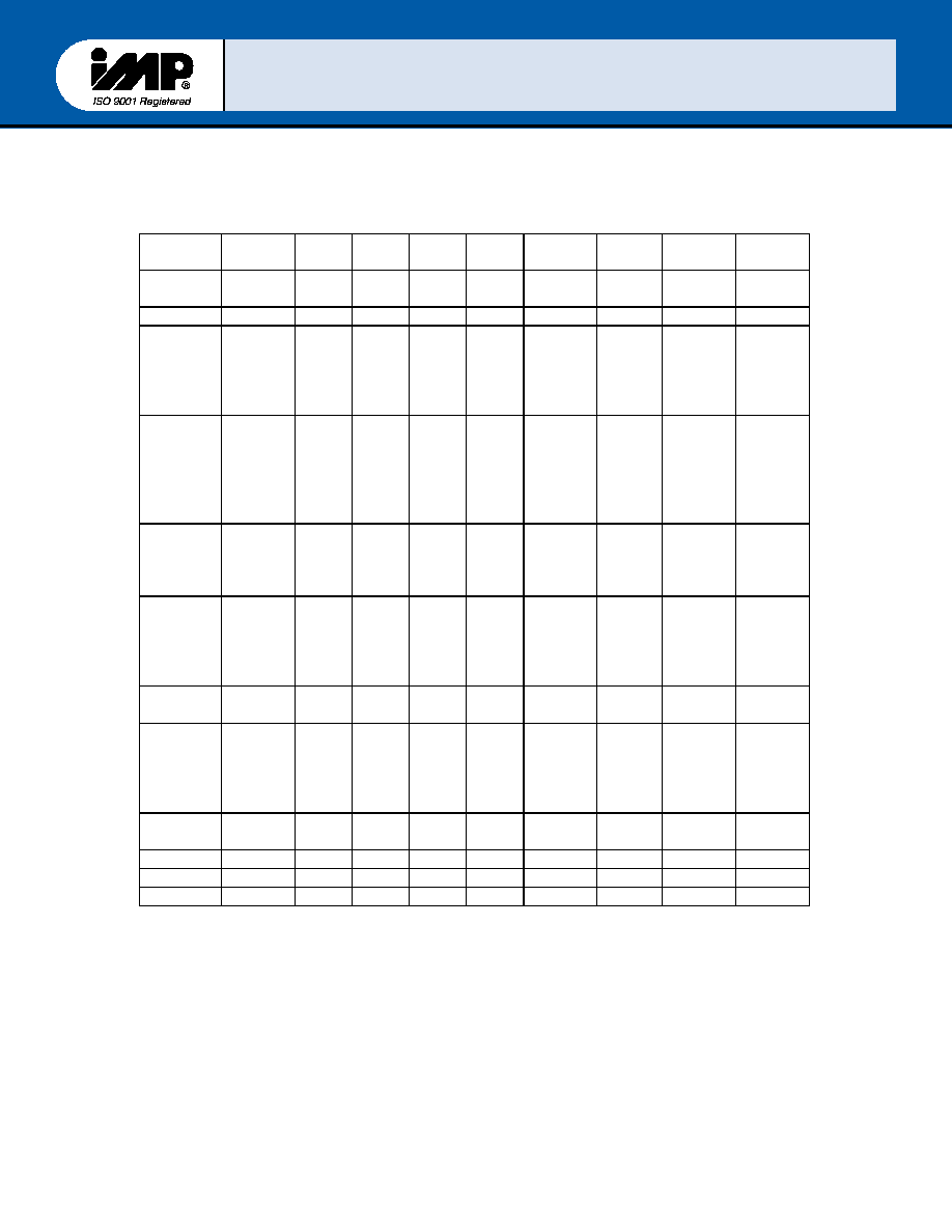
IMP16C554 ACCESSIBLE REGISTERS
A2A1A0 Registe
r
BIT-7 BIT-6 BIT-5 BIT-4 BIT-3 BIT-2
BIT-1 BIT-0
0 0 0
RHR
bit-7
bit-6
bit-5
bit-4
bit-3
bit-2
bit-1 bit-0
0 0 0
THR
bit-7
bit-6
bit-5
bit-4
bit-3
bit-2
bit-1
bit-0
0 0 1
IER
0
0
0
0
Modem
status
interrup
t
Receiv
e line
status
interru
pt
Transmi
t
holding
register
Receive
holding
register
0 1 0
FCR
RCV
R
trigge
r
(MSB
)
RCV
R
trigge
r
(LSB)
0
0
DMA
Mode
select
XMITF
IFO
reset
RCVRF
IFO
reset
FIFO
enable
0 1 0
ISR
0/FIF
Os
enabl
ed
0/FIF
Os
enabl
ed
0
0
int
priority
bit-2
Int
priority
bit-1
Int
priority
bit-0
Int
status
0 1 1
LCR
Divis
or
latch
enabl
e
Set
break
Set
parity
Even
parity
Parity
enable
Stop
bits
Word
length
bit-1
Word
length
bit-0
1 0 0
MCR
0
0
0
Loop
back
INT
enable
Not
used
RTS* DTR*
1 0 1
LSR
o/FIF
O
error
trans
empt
y
trans
holdi
ng
empt
y
break
interr
upt
framing
error
parity
error
overrun
error
receive
data
ready
1 1 0
MSR
CD
RI
DSR
CTS
delta
CD*
delta
RI*
delta
DSR*
delta
CTS*
1 1 1
SPR
bit-7
bit-6
bit-5
bit-4
bit-3
bit-2
bit-1
bit-0
0 0 0
DLL
bit-7
bit-6
bit-5
bit-4
bit-3
bit-2
bit-1
bit-0
0 0 1
DLM
bit-15 bit-14 bit-13 bit-12 bit-11
bit-10
bit-9
bit-8
DLL and DLM are accessible only when LCR bit-7 is set to "1".
5
408-432-9100/www.impweb.com © 2002 IMP, Inc.
IMP16C554
IMP16C554