 | –≠–ª–µ–∫—Ç—Ä–æ–Ω–Ω—ã–π –∫–æ–º–ø–æ–Ω–µ–Ω—Ç: IMP2525-2 | –°–∫–∞—á–∞—Ç—å:  PDF PDF  ZIP ZIP |
Document Outline
- Front Cover
- IMP2525
- IMP2525A
- IMP2526
USB Power Switch
IMP2525
IMP2525
USB High-Side Power Switch
IMP2525A
IMP2525A
Low-Resistance, USB High-Side Power Switch
IMP2526
IMP2526
Dual USB High-Side Power Switch
POWER
MANAGEMENT
408-432-9100/www.impweb.com
2
408-432-9100/www.impweb.com
©
1999 IMP, Inc.
USB P
USB P
o
o
w
w
er Switc
er Switc
h Pr
h Pr
oduct Guide
oduct Guide
Product Selection Guide
r
e
b
m
u
N
t
r
a
P
e
p
y
T
e
g
a
k
c
a
P
"
N
O
"
h
c
t
i
w
S
e
c
n
a
t
s
i
s
e
R
e
l
b
a
n
E
c
i
g
o
L
e
g
a
t
l
o
v
r
e
d
n
U
t
u
o
k
c
o
L
t
n
e
r
r
u
C
t
i
m
i
L
l
a
m
r
e
h
T
n
w
o
d
t
u
h
S
g
a
l
F
t
l
u
a
F
M
B
1
-
A
5
2
5
2
P
M
I
e
l
g
n
i
S
O
S
,
n
i
p
-
8
0
7
0
.
0
H
G
I
H
∑
∑
∑
∑
M
B
2
-
A
5
2
5
2
P
M
I
e
l
g
n
i
S
O
S
,
n
i
p
-
8
0
7
0
.
0
W
O
L
∑
∑
∑
∑
N
B
1
-
A
5
2
5
2
P
M
I
e
l
g
n
i
S
P
I
D
,
n
i
p
-
8
0
7
0
.
0
H
G
I
H
∑
∑
∑
∑
N
B
2
-
A
5
2
5
2
P
M
I
e
l
g
n
i
S
P
I
D
,
n
i
p
-
8
0
7
0
.
0
W
O
L
∑
∑
∑
∑
M
B
1
-
5
2
5
2
P
M
I
e
l
g
n
i
S
O
S
,
n
i
p
-
8
4
1
.
0
H
G
I
H
∑
∑
∑
∑
M
B
2
-
5
2
5
2
P
M
I
e
l
g
n
i
S
O
S
,
n
i
p
-
8
4
1
.
0
W
O
L
∑
∑
∑
∑
N
B
1
-
5
2
5
2
P
M
I
e
l
g
n
i
S
P
I
D
,
n
i
p
-
8
4
1
.
0
H
G
I
H
∑
∑
∑
∑
N
B
2
-
5
2
5
2
P
M
I
e
l
g
n
i
S
P
I
D
,
n
i
p
-
8
4
1
.
0
W
O
L
∑
∑
∑
∑
M
B
1
-
6
2
5
2
P
M
I
l
a
u
D
O
S
,
n
i
p
-
8
4
1
.
0
H
G
I
H
∑
∑
∑
∑
M
B
2
-
6
2
5
2
P
M
I
l
a
u
D
O
S
,
n
i
p
-
8
4
1
.
0
W
O
L
∑
∑
∑
∑
N
B
1
-
6
2
5
2
P
M
I
l
a
u
D
P
I
D
,
n
i
p
-
8
4
1
.
0
H
G
I
H
∑
∑
∑
∑
N
B
2
-
6
2
5
2
P
M
I
l
a
u
D
P
I
D
,
n
i
p
-
8
4
1
.
0
W
O
L
∑
∑
∑
∑
1
0
L
E
S
B
S
U
All devices are pin-compatible with the MIC2525/2526 devices. Compared to the Micrel MIC2525, the enhanced IMP2525A has a 50% lower "ON"
resistance.
2525A_03.eps
OUT
8
6
IN
GND
7
3
FLG
2
EN
1
Logic,
Charge
Pump
2525_03.eps
OUT
8
6
IN
GND
7
3
FLG
2
EN
1
Logic,
Charge
Pump
2526_03.eps
OUTA
8
IN
GND
7
6
FLGA
2
ENA
1
Logic,
Charge
Pump
OUTB
5
ENB
4
FLGB
3
Logic,
Charge
Pump
IMP2526
Pin Configuration Schematic
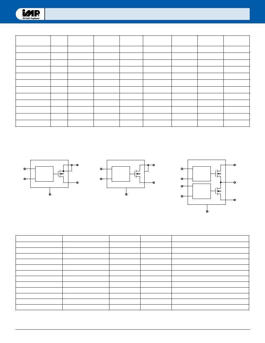
Product Cross Reference Guide
r
e
b
m
u
N
t
r
a
P
l
e
r
c
i
M
r
e
b
m
u
N
t
r
a
P
P
M
I
e
p
y
T
e
g
a
k
c
a
P
e
c
n
a
t
s
i
s
e
R
"
N
O
"
h
c
t
i
w
S
M
B
1
-
A
5
2
5
2
C
I
M
M
B
1
-
A
5
2
5
2
P
M
I
e
l
g
n
i
S
O
S
,
n
i
p
-
8
0
7
0
.
0
4
1
.
0
.
s
v
5
2
5
2
l
e
r
c
i
M
r
o
f
M
B
2
-
A
5
2
5
2
C
I
M
M
B
2
-
A
5
2
5
2
P
M
I
e
l
g
n
i
S
O
S
,
n
i
p
-
8
0
7
0
.
0
4
1
.
0
.
s
v
5
2
5
2
l
e
r
c
i
M
r
o
f
N
B
1
-
A
5
2
5
2
C
I
M
N
B
1
-
A
5
2
5
2
P
M
I
e
l
g
n
i
S
P
I
D
,
n
i
p
-
8
0
7
0
.
0
4
1
.
0
.
s
v
5
2
5
2
l
e
r
c
i
M
r
o
f
N
B
2
-
A
5
2
5
2
C
I
M
N
B
2
-
A
5
2
5
2
P
M
I
e
l
g
n
i
S
P
I
D
,
n
i
p
-
8
0
7
0
.
0
4
1
.
0
.
s
v
5
2
5
2
l
e
r
c
i
M
r
o
f
M
B
1
-
5
2
5
2
C
I
M
M
B
1
-
5
2
5
2
P
M
I
e
l
g
n
i
S
O
S
,
n
i
p
-
8
4
1
.
0
M
B
2
-
5
2
5
2
C
I
M
M
B
2
-
5
2
5
2
P
M
I
e
l
g
n
i
S
O
S
,
n
i
p
-
8
4
1
.
0
N
B
1
-
5
2
5
2
C
I
M
N
B
1
-
5
2
5
2
P
M
I
e
l
g
n
i
S
P
I
D
,
n
i
p
-
8
4
1
.
0
N
B
2
-
5
2
5
2
C
I
M
N
B
2
-
5
2
5
2
P
M
I
e
l
g
n
i
S
P
I
D
,
n
i
p
-
8
4
1
.
0
M
B
1
-
6
2
5
2
C
I
M
M
B
1
-
6
2
5
2
P
M
I
l
a
u
D
O
S
,
n
i
p
-
8
4
1
.
0
M
B
2
-
6
2
5
2
C
I
M
M
B
2
-
6
2
5
2
P
M
I
l
a
u
D
O
S
,
n
i
p
-
8
4
1
.
0
N
B
1
-
6
2
5
2
C
I
M
N
B
1
-
6
2
5
2
P
M
I
l
a
u
D
P
I
D
,
n
i
p
-
8
4
1
.
0
N
B
2
-
6
2
5
2
C
I
M
N
B
2
-
6
2
5
2
P
M
I
l
a
u
D
P
I
D
,
n
i
p
-
8
4
1
.
0
2
0
f
e
r
X
B
S
U

©
1999 IMP, Inc.
408-432-9100/www.impweb.com
1
Key Features
Applications
N USB power management
N USB hosts and self-powered hubs
N Battery-charger circuits and power supplies
N Meets or exceeds USB Rev. 1.1 and 2.0
specification
N Low MOSFET R
ON
(0.14
at 3V)
N 2.7V to 5.5V input operation
N Current limiting
N Soft-start turn-on (1ms) prevents turn-on glitches
N 500mA continuous load current
N MOSFET short-circuit current limit (1.25A max)
N Low supply current
≠ 110µA ON state current, 1µA OFF state current
N Active-LOW or Active-HIGH Enable input
N 3.3V or 5V logic compatibility
N Fault Flag indicates three fault conditions:
≠ Undervoltage
≠ Current limit
≠ Thermal shutdown
N Open-drain Fault Flag output
N 2.4V Undervoltage Lockout (UVLO)
N Pin compatible with the Micrel MIC2525
Block Diagrams
IMP2525
IMP2525
P
OWER
M
ANAGEMENT
USB High-Side P
USB High-Side P
o
o
w
w
er Switc
er Switc
h
h
≠ Sing
≠ Sing
le switc
le switc
h
h
≠ 0.
≠ 0.
1
1
4
4
"ON" r
"ON" r
esis
esis
t
t
ance at 3V
ance at 3V
≠ MIC2525 pin com
≠ MIC2525 pin com
patible
patible
The IMP2525 high-side power switch IC is designed for self-powered
and bus-powered Universal Serial Bus (USB) power supply and power
management applications. The IMP2525 conforms to USB standards
with a low output switch ON-resistance (R
ON
) and minimal voltage drop
across the switch. The fault current is limited to 750mA typically, and
a flag output conveys fault conditions to the local USB controller.
The IMP2525 provides a "Soft-Start" function that ramps up the ON-
current to eliminate any excessive voltage drop on the input side that
could occur due to charging a capacitive load in bus-powered applica-
tions. Self-monitoring features include thermal shutdown to prevent
catastrophic switch failure from high-current loads and undervoltage
lockout (UVLO) that insures that the device remains off unless there is a
valid supply voltage present. The Enable input logic can be interfaced
with both 3.3V and 5V logic. Both active-HIGH and active-LOW enable
logic versions are available. The IMP2525 devices are available in 8-pin
DIP and 8-pin SO packages.
IMP offers a complete family of USB power management products. For
dual-switch applications see the IMP2526 data sheet and for quad-switch
application, see the IMP2524. The single-switch IMP2525A features a
50% lower switch resistance, 0.07
.
2525_01.eps
OUT
NC/OUT
8
6
FLG
2
GND
3
IMP2525
Power
Switch
Gate
Control
Current
Limit
1.2V
Reference
UVLO
Thermal
Shutdown
Oscillator
EN
1
IN
7
Charge
Pump
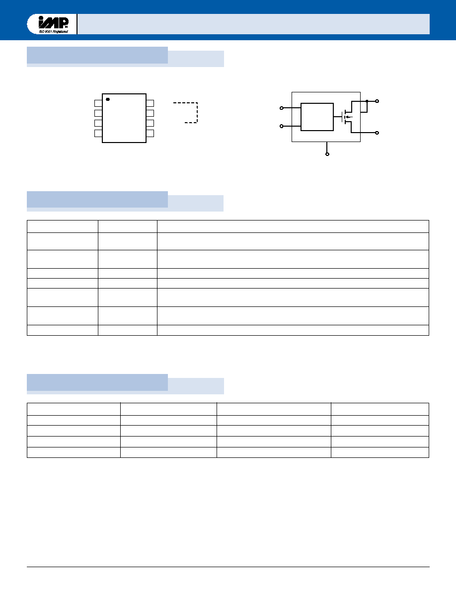
2
408-432-9100/www.impweb.com
©
1999 IMP, Inc.
Pin Descriptions
Ordering Information
Pin Configuration
IMP2525
IMP2525
4
NC
3
GND
2
FLG
1
EN
5
NC
6
NC/OUT
*Connect pins 6 and 8 for MIC2525 compatibility
7
IN
*
8
OUT
2525_02.eps
IMP2525
SO/DIP
2525_03.eps
OUT
8
6
IN
GND
7
3
FLG
2
EN
1
Logic,
Charge
Pump
Pin Number
Name
Function
1
EN
Enable input. This pin is the MOSFET switch driver logic input. Both active-HIGH
(-1 suffix) and active-LOW (-2 suffix) logic devices are available.
2
FLG
Fault flag output. This open-drain output goes into an active-LOW state in response to
undervoltage, current limit or thermal shutdown conditions.
3
GND
Ground. Power supply return for the internal circuitry of the IC.
4, 5
NC
No connection. These pins have no internal connections to the device.
6
NC/OUT
No connection. This pin has no internal connection to the device. Connect pins 6 and 8 to
maintain pin-compatibility with the MIC2525.
7
IN
Positive power supply voltage input. This is the switching MOSFET drain connection
as well as the positive supply for the IC.
8
OUT
MOSFET source. The output pin supplies power to the load.
Part Number
Enable Logic
Temperature Range
Pins-Package
IMP2525-1BM
Active HIGH
≠ 40
∞C to +85∞C
8-SO
IMP2525-2BM
Active LOW
≠ 40
∞C to +85∞C
8-SO
IMP2525-1BN
Active HIGH
≠ 40
∞C to +85∞C
8-DIP
IMP2525-2BN
Active LOW
≠ 40
∞C to +85∞C
8-DIP

©
1999 IMP, Inc.
408-432-9100/www.impweb.com
3
IMP2525
IMP2525
Absolute Maximum Ratings
Electrical Characteristics
Supply Voltage . . . . . . . . . . . . . . . . . . . . . . . . . . +6.0V
Fault Flag Voltage . . . . . . . . . . . . . . . . . . . . . . +6.0V
Fault Flag Current . . . . . . . . . . . . . . . . . . . . . . 50mA
Output Voltage . . . . . . . . . . . . . . . . . . . . . . . . . +6.0V
Output Current . . . . . . . . . . . . . . . . . . . . . . . . . Internally Limited
Enable Input . . . . . . . . . . . . . . . . . . . . . . . . . . . ≠0.3V to 12V
Storage Temperature . . . . . . . . . . . . . . . . . . . . . ≠65
∞C to +150∞C
Lead Temperature (Soldering, 5 sec.) . . . . . . . 260
∞C
Package Thermal Resistance
SO (
JA
) . . . . . . . . . . . . . . . . . . . . . . . . . . . . . 120
∞C/W
DIP(
JA
) . . . . . . . . . . . . . . . . . . . . . . . . . . . . 130
∞C/W
Note: All voltages are referenced to GND.
These are stress ratings only and functional operation is not
implied. Exposure to absolute maximum ratings for prolonged
time periods may affect device reliability.
Parameter
SymbolConditions
Min
Typ
Max
Units
Supply Voltage Range
V
IN
T
A
= ≠ 40
∞C to +85∞C
2.7
5.5
V
Operating Temperature Range
T
A
≠ 40
85
∞C
Supply Current
I
IN OFF
Switch OFF, No load
0.75
5
µA
Switch OFF
V
ENOFF
0.8V, V
ENON
2.4V IMP2525-1
V
ENON
0.8V, V
ENOFF
2.4V IMP2525-2
Supply Current
I
IN ON
Switch ON, No load
110
160
µA
Switch ON
V
ENOFF
0.8V, V
ENON
2.4V IMP2525-1
V
ENON
0.8V, V
ENOFF
2.4V IMP2525-2
Enable Input Threshold
V
ENH
LOW to HIGH ("0" to "1") Enable Voltage, Note 1, 2
2.1
2.4
V
V
ENL
HIGH to LOW ("1" to "0") Enable Voltage, Note 1, 2
0.8
1.9
Enable Input Current
I
EN
V
EN
= 0V to 5.5V
≠1
±0.01
1
µA
Enable Input Capacitance
C
EN
1
pF
Switch ON Resistance
R
ON
V
IN
= 5V, I
OUT
= 500mA
0.1
0.14
V
IN
= 3.3V, I
OUT
= 500mA
0.14
0.18
Output Turn-On Delay
T
DON
R
L
= 10
0.25
ms
Output Turn-On Rise Time
T
RON
R
L
= 10
1
ms
Output Turn-Off Delay
T
DOFF
R
L
= 10
, Note 2
1
20
µs
Output Turn-Off Fall Time
T
FOFF
R
L
= 10
, Note 2
1
20
µs
Output Leakage Current
I
OFF
10
µA
Short-circuit Current Limit
I
SC
0.50
0.75
1.25
A
Overtemperature Shutdown
T
J
increasing
135
∞C
Threshold T
J
decreasing 125
Error Flag Output Resistance
R
FLAG
V
IN
= 5V, I
L
= 10mA
10
25
V
IN
= 3.3V, I
L
= 10mA
15
40
Error Flag Output Current
I
FLAG
V
FLAG
= 5V
0.01
1
µA
UVLO Threshold
V
UVLO
V
IN
Increasing
2.5
V
V
IN
Decreasing
2.3
Unless otherwise noted, V
IN
= 5V and T
A
= 25∞C.
Notes 1. Switch OFF is V
EN
0.8V and Switch ON is V
EN
2.4V for the IMP2525-1. Switch OFF is V
EN
2.4V and Switch ON is V
EN
0.8V
for the IMP2525-2. The Enable input has approximately 200mV of hysteresis.
2. Over operating temperature range, ≠40
∞C T
A
85∞C.