 | –≠–ª–µ–∫—Ç—Ä–æ–Ω–Ω—ã–π –∫–æ–º–ø–æ–Ω–µ–Ω—Ç: BCR142 | –°–∫–∞—á–∞—Ç—å:  PDF PDF  ZIP ZIP |

Aug-29-2003
1
BCR142...
NPN Silicon Digital Transistor
∑
Switching circuit, inverter, interface circuit,
driver circuit
∑
Built in bias resistor (R
1
=22k
, R
2
=47k
)
BCR142/F/L3
BCR142T/W
EHA07184
3
2
1
C
E
B
R
1
R
2
Type
Marking
Pin Configuration
Package
BCR142
BCR142F
BCR142FL3
BCR142T
BCR142W
WZs
WZs
WZ
WZs
WZs
1=B
1=B
1=B
1=B
1=B
2=E
2=E
2=E
2=E
2=E
3=C
3=C
3=C
3=C
3=C
-
-
-
-
-
-
-
-
-
-
-
-
-
-
-
SOT23
TSFP-3
TSLP-3-4
SC75
SOT323

Aug-29-2003
2
BCR142...
Maximum Ratings
Parameter
Symbol
Value
Unit
Collector-emitter voltage
V
CEO
50
V
Collector-base voltage
V
CBO
50
Emitter-base voltage
V
EBO
10
Input on voltage
V
i(on)
30
Collector current
I
C
100
mA
Total power dissipation-
BCR142, T
S
102∞C
BCR142F, T
S
128∞C
BCR142L3, T
S
135∞C
BCR142T, T
S
109∞C
BCR142W, T
S
124∞C
P
tot
200
250
250
250
250
mW
Junction temperature
T
j
150
∞C
Storage temperature
T
stg
-65 ... 150
Thermal Resistance
Parameter
Symbol
Value
Unit
Junction - soldering point
1)
BCR142
BCR142F
BCR142L3
BCR142T
BCR142W
R
thJS
240
90
60
165
105
K/W
1For calculation of R
thJA
please refer to Application Note Thermal Resistance

Aug-29-2003
3
BCR142...
Electrical Characteristics at T
A
= 25∞C, unless otherwise specified
Parameter
Symbol
Values
Unit
min.
typ.
max.
DC Characteristics
Collector-emitter breakdown voltage
I
C
= 100 µA, I
B
= 0
V
(BR)CEO
50
-
-
V
Collector-base breakdown voltage
I
C
= 10 µA, I
E
= 0
V
(BR)CBO
50
-
-
Collector-base cutoff current
V
CB
= 40 V, I
E
= 0
I
CBO
-
-
100
nA
Emitter-base cutoff current
V
EB
= 10 V, I
C
= 0
I
EBO
-
-
227
µA
DC current gain-
1)
I
C
= 5 mA, V
CE
= 5 V
h
FE
70
-
-
-
Collector-emitter saturation voltage
1)
I
C
= 10 mA, I
B
= 0.5 mA
V
CEsat
-
-
0.3
V
Input off voltage
I
C
= 100 µA, V
CE
= 5 V
V
i(off)
0.5
-
1.2
Input on voltage
I
C
= 2 mA, V
CE
= 0.3 V
V
i(on)
0.8
-
2.5
Input resistor
R
1
15
22
29
k
Resistor ratio
R
1
/R
2
0.42
0.47
0.52
-
AC Characteristics
Transition frequency
I
C
= 10 mA, V
CE
= 5 V, f = 100 MHz
f
T
-
150
-
MHz
Collector-base capacitance
V
CB
= 10 V, f = 1 MHz
C
cb
-
3
-
pF
1Pulse test: t < 300µs; D < 2%
Aug-29-2003
4
BCR142...
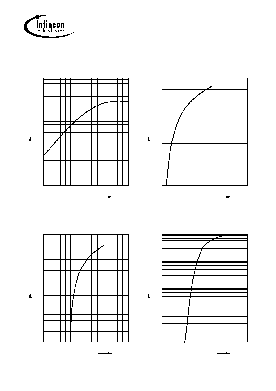
DC current gain h
FE
=
(I
C
)
V
CE
= 5V (common emitter configuration)
10
-1
10
0
10
1
10
2
mA
I
C
0
10
1
10
2
10
3
10
-
h
FE
Collector-emitter saturation voltage
V
CEsat
=
(I
C
), h
FE
= 20
0
0.2
0.4
0.6
V
1
V
CEsat
0
10
1
10
2
10
mA
I
C
Input on Voltage V
i
(on)
=
(I
C
)
V
CE
= 0.3V (common emitter configuration)
10
-1
10
0
10
1
10
2
V
V
i(on)
-1
10
0
10
1
10
2
10
mA
I
C
Input off voltage V
i(off)
=
(I
C
)
V
CE
= 5V (common emitter configuration)
0
0.5
1
1.5
V
2.5
V
i(off)
-3
10
-2
10
-1
10
0
10
1
10
mA
I
C

Aug-29-2003
5
BCR142...
Total power dissipation P
tot
=
(T
S
)
BCR142
0
20
40
60
80
100
120 ∞C
150
T
S
0
50
100
150
200
mW
300
P
tot
Total power dissipation P
tot
=
(T
S
)
BCR142F
0
20
40
60
80
100
120 ∞C
150
T
S
0
50
100
150
200
mW
300
P
tot
Total power dissipation P
tot
=
(T
S
)
BCR142L3
0
20
40
60
80
100
120 ∞C
150
T
S
0
50
100
150
200
mW
300
P
tot
Total power dissipation P
tot
=
(T
S
)
BCR142T
0
20
40
60
80
100
120 ∞C
150
T
S
0
50
100
150
200
mW
300
P
tot

Aug-29-2003
6
BCR142...
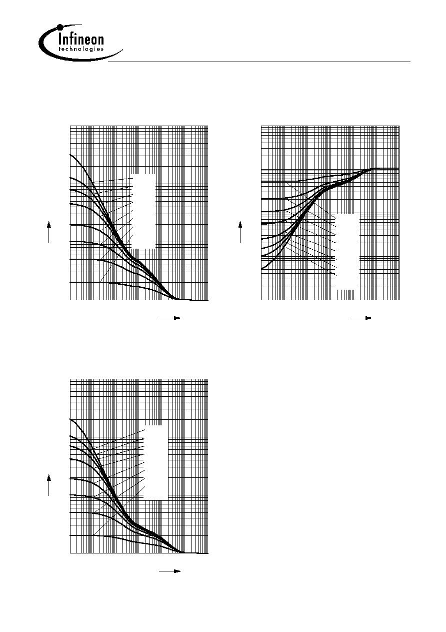
Total power dissipation P
tot
=
(T
S
)
BCR142W
0
20
40
60
80
100
120 ∞C
150
T
S
0
50
100
150
200
mW
300
P
tot
Permissible Pulse Load
P
totmax
/P
totDC
=
(t
p
)
BCR142
10
-6
10
-5
10
-4
10
-3
10
-2
10
0
s
t
p
0
10
1
10
2
10
3
10
-
P
totmax
/
P
totDC
D = 0
0.005
0.01
0.02
0.05
0.1
0.2
0.5
Permissible Pulse Load R
thJS
=
(t
p
)
BCR142
10
-6
10
-5
10
-4
10
-3
10
-2
10
0
s
t
p
-1
10
0
10
1
10
2
10
3
10
K/W
R
thJS
0.5
0.2
0.1
0.05
0.02
0.01
0.005
D = 0
Permissible Puls Load R
thJS
=
(t
p
)
BCR142F
10
-6
10
-5
10
-4
10
-3
10
-2
10
0
s
t
p
-1
10
0
10
1
10
2
10
K/W
R
thJS
D=0.5
0.2
0.1
0.05
0.02
0.01
0.005
0
Aug-29-2003
7
BCR142...
Permissible Pulse Load
P
totmax
/P
totDC
=
(t
p
)
BCR142F
10
-6
10
-5
10
-4
10
-3
10
-2
10
0
s
t
p
0
10
1
10
2
10
3
10
P
totmax
/
P
totDC
D=0
0.005
0.01
0.02
0.05
0.1
0.2
0.5
Permissible Puls Load R
thJS
=
(t
p
)
BCR142L3
10
-7
10
-6
10
-5
10
-4
10
-3
10
-2
10
0
s
tp
-1
10
0
10
1
10
2
10
R
thJS
0.5
0.2
0.1
0.05
0.02
0.01
0.005
D = 0
Permissible Pulse Load
P
totmax
/P
totDC
=
(t
p
)
BCR142L3
10
-7
10
-6
10
-5
10
-4
10
-3
10
-2
10
0
s
t
p
0
10
1
10
2
10
3
10
P
totmax
/
P
totDC
D = 0
0.005
0.01
0.02
0.05
0.1
0.2
0.5
Permissible Puls Load R
thJS
=
(t
p
)
BCR142T
10
-6
10
-5
10
-4
10
-3
10
-2
10
0
s
t
p
-1
10
0
10
1
10
2
10
3
10
K/W
R
thJS
D=0.5
0.2
0.1
0.05
0.02
0.01
0.005
0
Aug-29-2003
8
BCR142...
Permissible Pulse Load
P
totmax
/P
totDC
=
(t
p
)
BCR142T
10
-6
10
-5
10
-4
10
-3
10
-2
10
0
s
t
p
0
10
1
10
2
10
3
10
P
totmax
/
P
totDC
D=0
0.005
0.01
0.02
0.05
0.1
0.2
0.5
Permissible Puls Load R
thJS
=
(t
p
)
BCR142W
10
-6
10
-5
10
-4
10
-3
10
-2
10
0
s
t
p
-1
10
0
10
1
10
2
10
3
10
K/W
R
thJS
0.5
0.2
0.1
0.05
0.02
0.01
0.005
D = 0
Permissible Pulse Load
P
totmax
/P
totDC
=
(t
p
)
BCR142W
10
-6
10
-5
10
-4
10
-3
10
-2
10
0
s
t
p
0
10
1
10
2
10
3
10
-
P
totmax
/
P
totDC
D = 0
0.005
0.01
0.02
0.05
0.1
0.2
0.5