 | ÐлекÑÑоннÑй компоненÑ: BCR22PN | СкаÑаÑÑ:  PDF PDF  ZIP ZIP |
Äîêóìåíòàöèÿ è îïèñàíèÿ www.docs.chipfind.ru
BCR22PN
Dec-13-2001
1
NPN/PNP Silicon Digital Transistor Array
Switching circuit, inverter, interface circuit,
driver circuit
Two (galvanic) internal isolated NPN/PNP
Transistors in one package
Built in bias resistor (R
1
=22k
, R
2
=22k
)
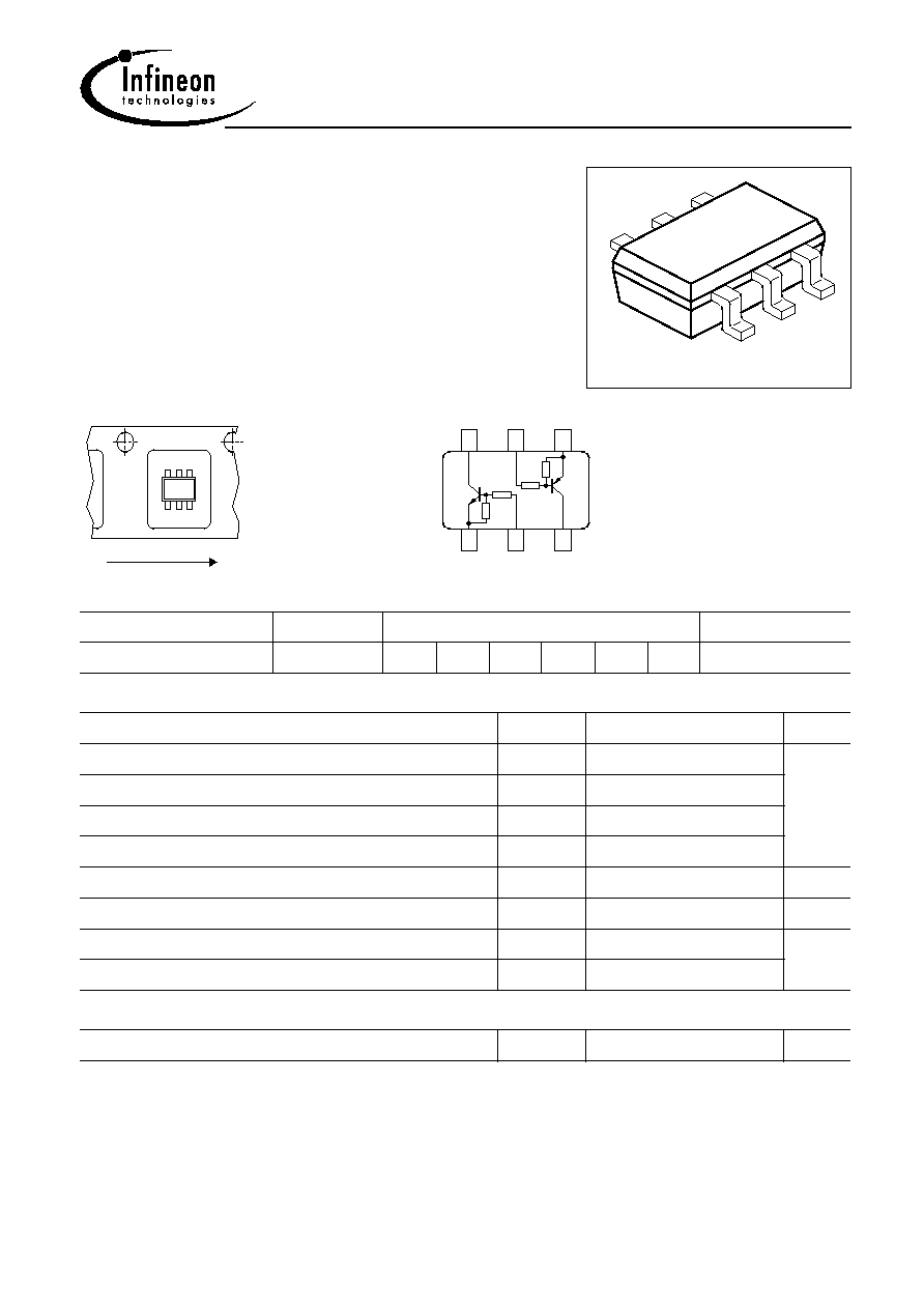
Tape loading orientation
VPS05604
6
3
1
5
4
2
EHA07193
1 2 3
4
5
6
W1s
Direction of Unreeling
Top View
Marking on SOT-363 package
(for example W1s)
corresponds to pin 1 of device
Position in tape: pin 1
opposite of feed hole side
EHA07176
6
5
4
3
2
1
C1
B2
E2
C2
B1
E1
1
R
R
2
R
1
R
2
TR1
TR2
Type
Marking
Pin Configuration
Package
BCR22PN
WPs
1=E1 2=B1 3=C2 4=E2 5=B2 6=C1 SOT363
Maximum Ratings
Parameter
Symbol
Value
Unit
Collector-emitter voltage
V
CEO
50
V
Collector-base voltage
V
CBO
50
Emitter-base voltage
V
EBO
10
Input on Voltage
V
i(on)
30
DC collector current
I
C
100
mA
Total power dissipation
,
T
S
= 115 °C
P
tot
250
mW
Junction temperature
T
j
150
°C
Storage temperature
T
stg
-65 ... 150
Thermal Resistance
Junction - soldering point
1)
R
thJS
140
K/W
1For calculation of R
thJA
please refer to Application Note Thermal Resistance

BCR22PN
Dec-13-2001
2
Electrical Characteristics at T
A
=25°C, unless otherwise specified
Parameter
Symbol
Values
Unit
min.
typ.
max.
DC Characteristics
Collector-emitter breakdown voltage
I
C
= 100 µA,
I
B
= 0
V
(BR)CEO
50
-
-
V
Collector-base breakdown voltage
I
C
= 10 µA,
I
E
= 0
V
(BR)CBO
50
-
-
Collector cutoff current
V
CB
= 40 V,
I
E
= 0
I
CBO
-
-
100
nA
Emitter cutoff current
V
EB
= 10 V,
I
C
= 0
I
EBO
-
-
350
µA
DC current gain 1)
I
C
= 5 mA,
V
CE
= 5 V
h
FE
50
-
-
-
Collector-emitter saturation voltage1)
I
C
= 10 mA,
I
B
= 0.5 mA
V
CEsat
-
-
0.3
V
Input off voltage
I
C
= 100 µA,
V
CE
= 5 V
V
i(off)
0.8
-
1.5
Input on Voltage
I
C
= 2 mA,
V
CE
= 0.3 V
V
i(on)
1
-
2.5
Input resistor
R
1
15
22
29
k
Resistor ratio
R
1
/R
2
0.9
1
1.1
-
AC Characteristics
Transition frequency
I
C
= 10 mA,
V
CE
= 5 V,
f
= 100 MHz
f
T
-
130
-
MHz
Collector-base capacitance
V
CB
= 10 V,
f
= 1 MHz
C
cb
-
3
-
pF
1) Pulse test: t < 300
s; D < 2%
BCR22PN
Dec-13-2001
3
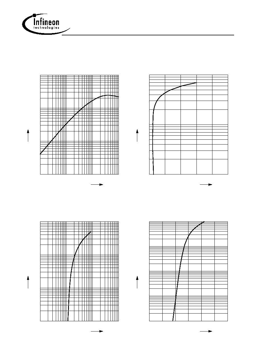
NPN Type
DC Current Gain h
FE
= f (I
C
)
V
CE
= 5V (common emitter configuration)
10
-1
10
0
10
1
10
2
mA
I
C
0
10
1
10
2
10
3
10
-
h
FE
Collector-Emitter Saturation Voltage
V
CEsat
= f (I
C
), h
FE
= 20
0.0
0.2
0.4
0.6
V
1.0
V
CEsat
0
10
1
10
2
10
mA
I
C
Input on Voltage V
i(on)
= f (I
C
)
V
CE
= 0.3V (common emitter configuration)
10
-1
10
0
10
1
10
2
V
V
i(on)
-1
10
0
10
1
10
2
10
mA
I
C
Input off voltage V
i(off)
= f (I
C
)
V
CE
= 5V (common emitter configuration)
0.0
0.5
1.0
1.5
2.0
V
3.0
V
i(off)
-3
10
-2
10
-1
10
0
10
1
10
mA
I
C
BCR22PN
Dec-13-2001
4
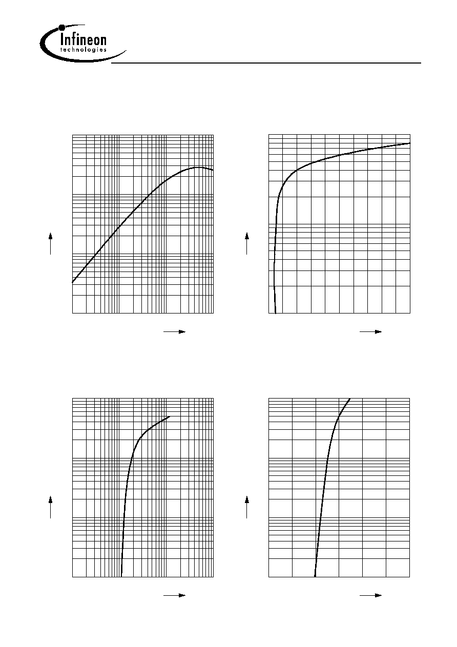
PNP Type
Collector-Emitter Saturation Voltage
V
CEsat
= f (I
C
), h
FE
= 20
0.0 0.1 0.2 0.3 0.4 0.5 0.6 0.7 0.8
V
1.0
V
CEsat
0
10
1
10
2
10
mA
I
C
DC Current Gain h
FE
= f (I
C
)
V
CE
= 5V (common emitter configuration)
10
-1
10
0
10
1
10
2
mA
I
C
0
10
1
10
2
10
3
10
-
h
FE
Input off voltage
V
i(off)
= f (I
C
)
V
CE
= 5V (common emitter configuration)
0.0
0.5
1.0
1.5
2.0
V
3.0
V
i(off)
-2
10
-1
10
0
10
1
10
mA
I
C
Input on Voltage V
i(on)
= f (I
C
)
V
CE
= 0.3V (common emitter configuration)
10
-1
10
0
10
1
10
2
V
V
i(on)
-1
10
0
10
1
10
2
10
mA
I
C
BCR22PN
Dec-13-2001
5
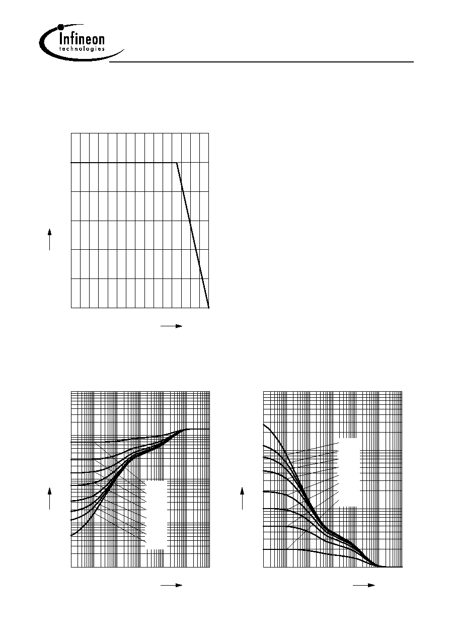
Total power dissipation P
tot
= f (T
S
)
0
20
40
60
80
100
120 °C
150
T
S
0
50
100
150
200
mW
300
P
tot
Permissible Pulse Load R
thJS
= f (t
p
)
10
-6
10
-5
10
-4
10
-3
10
-2
10
0
s
t
p
-1
10
0
10
1
10
2
10
3
10
K/W
R
thJS
0.5
0.2
0.1
0.05
0.02
0.01
0.005
D = 0
Permissible Pulse Load
P
totmax
/ P
totDC
= f (t
p
)
10
-6
10
-5
10
-4
10
-3
10
-2
10
0
s
t
p
0
10
1
10
2
10
3
10
-
P
totmax
/ P
totDC
D = 0
0.005
0.01
0.02
0.05
0.1
0.2
0.5