 | –≠–ª–µ–∫—Ç—Ä–æ–Ω–Ω—ã–π –∫–æ–º–ø–æ–Ω–µ–Ω—Ç: BCX53-10 | –°–∫–∞—á–∞—Ç—å:  PDF PDF  ZIP ZIP |
BCX51...BCX53
Feb-10-2004
1
PNP Silicon AF Transistors
∑
For AF driver and output stages
∑
High collector current
∑
Low collector-emitter saturation voltage
∑
Complementary types: BCX54...BCX56 (NPN)
2
1
3
VPS05162
2
Type
Marking
Pin Configuration
Package
BCX51
BCX51-10
BCX51-16
BCX52
BCX52-10
BCX52-16
BCX53
BCX53-10
BCX53-16
AA
AC
AD
AE
AG
AM
AH
AK
AL
1 = B
1 = B
1 = B
1 = B
1 = B
1 = B
1 = B
1 = B
1 = B
2 = C
2 = C
2 = C
2 = C
2 = C
2 = C
2 = C
2 = C
2 = C
3 = E
3 = E
3 = E
3 = E
3 = E
3 = E
3 = E
3 = E
3 = E
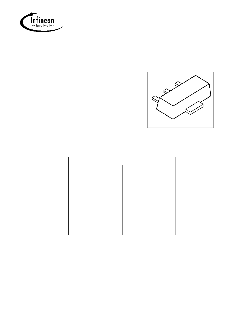
SOT89
SOT89
SOT89
SOT89
SOT89
SOT89
SOT89
SOT89
SOT89

BCX51...BCX53
Feb-10-2004
2
Maximum Ratings
Parameter
Symbol
BCX51
BCX52
BCX53 Unit
Collector-emitter voltage
V
CEO
45
60
80
V
Collector-base voltage
V
CBO
45
60
100
Emitter-base voltage
V
EBO
5
5
5
DC collector current
I
C
1
A
1.5
Peak collector current
I
CM
Base current
I
B
mA
100
I
BM
200
Peak base current
W
P
tot
Total power dissipation
,
T
S
= 130 ∞C
1
Junction temperature
150
∞C
T
j
T
stg
-65 ... 150
Storage temperature
Thermal Resistance
Junction - soldering point
1)
R
thJS
20
K/W
1For calculation of R
thJA
please refer to Application Note Thermal Resistance

BCX51...BCX53
Feb-10-2004
3
Electrical Characteristics at T
A
= 25∞C, unless otherwise specified.
Parameter
Symbol
Values
Unit
min.
typ.
max.
DC Characteristics
Collector-emitter breakdown voltage
I
C
= 10 mA,
I
B
= 0
BCX51
BCX52
BCX53
V
(BR)CEO
45
60
80
-
-
-
-
-
-
V
Collector-base breakdown voltage
I
C
= 100 µA,
I
E
= 0
BCX51
BCX52
BCX53
V
(BR)CBO
45
60
100
-
-
-
-
-
-
Emitter-base breakdown voltage
I
E
= 10 µA,
I
C
= 0
V
(BR)EBO
5
-
-
Collector cutoff current
V
CB
= 30 V,
I
E
= 0
I
CBO
-
-
100
nA
Collector cutoff current
V
CB
= 30 V,
I
E
= 0 ,
T
A
= 150 ∞C
I
CBO
-
-
20
µA
DC current gain 1)
I
C
= 5 mA,
V
CE
= 2 V
h
FE
25
-
-
-
DC current gain 1)
I
C
= 150 mA,
V
CE
= 2 V
BCX51...53
hFE-grp.10
hFE-grp.16
h
FE
40
63
100
-
100
160
250
160
250
DC current gain 1)
I
C
= 500 mA,
V
CE
= 2 V
h
FE
25
-
-
Collector-emitter saturation voltage1)
I
C
= 500 mA,
I
B
= 50 mA
V
CEsat
-
-
0.5
V
Base-emitter voltage 1)
I
C
= 500 mA,
V
CE
= 2 V
V
BE(ON)
-
-
1
AC Characteristics
-
MHz
f
T
-
Transition frequency
I
C
= 50 mA,
V
CE
= 10 V,
f
= 20 MHz
125
1) Pulse test: t
300
µ
s, D = 2%

BCX51...BCX53
Feb-10-2004
4
Collector current I
C
= f (V
BE
)
V
CE
= 2V
10
0
0.6
BCX 51...53
EHP00437
V
BE
10
mA
10
10
10
4
3
2
1
0
5
5
5
V
0.2
0.4
0.8
1.0
1.2
100
25
-50
C
∞C
∞C
∞C
Total power dissipation P
tot
= f(T
S
)
0
20
40
60
80
100
120 ∞C
150
T
S
0
0.1
0.2
0.3
0.4
0.5
0.6
0.7
0.8
0.9
1
W
1.2
P
tot
Transition frequency f
T
= f (I
C
)
V
CE
= 10V
10
10
10
10
BCX 51...53
EHP00439
f
mA
MHz
0
1
2
3
5
T
3
10
10
2
1
10
5
5
5
C
Permissible pulse load
P
totmax
/ P
totDC
= f (t
p
)
10
EHP00438
BCX 51...53
-6
0
10
5
D =
5
10
1
5
10
2
3
10
10
-5
10
-4
10
-3
10
-2
10
0
s
0
0.005
0.01
0.02
0.05
0.1
0.2
0.5
t
p
=
D
T
t
p
T
tot max
tot
P
DC
P
p
t

BCX51...BCX53
Feb-10-2004
5
Collector-emitter saturation voltage
I
C
= f (V
CEsat
), h
FE
= 10
0
0.4
0.8
BCX 51...53
EHP00441
V
CE sat
V
mA
10
4
1
10
10
10
2
10
10
3
10
C
5
5
5
10
0
0.2
0.6
100
25
-50
∞C
∞C
∞C
DC current gain h
FE
= f (I
C
)
V
CE
= 2V
10
10
10
10
BCX 51...53
EHP00440
h
mA
0
1
3
4
FE
3
10
10
2
0
10
5
5
10
1
2
10
5
100
25
-50
5
5
5
C
∞C
∞C
∞C
Collector cutoff current I
CBO
= f (T
A
)
V
CB
= 30V
10
0
50
100
150
BCX 51...53
EHP00442
T
A
5
10
10
nA
10
CB0
5
5
5
10
10
4
3
2
1
0
-1
max
typ
∞C
Base-emitter saturation voltage
I
C
= f (V
BEsat
), h
FE
= 10
10
0
0.6
BCX 51...53
EHP00443
V
BE sat
10
mA
10
10
10
4
3
2
1
0
5
5
5
V
0.2
0.4
0.8
1.0
1.2
100
25
-50
C
∞C
∞C
∞C