 | –≠–ª–µ–∫—Ç—Ä–æ–Ω–Ω—ã–π –∫–æ–º–ø–æ–Ω–µ–Ω—Ç: BF1005 | –°–∫–∞—á–∞—Ç—å:  PDF PDF  ZIP ZIP |

Feb-18-2004
1
BF1005...
Silicon N-Channel MOSFET Tetrode
∑
For low noise, high gain controlled
input stages up to 1 GHz
∑
Operating voltage 5V
∑
Integrated biasing network
EHA07215
GND
G1
G2
Drain
AGC
HF
Input
HF Output
+ DC
ESD
: Electrostatic discharge sensitive device, observe handling precaution!
Type
Package
Pin Configuration
Marking
BF1005
BF1005R
BF1005W*
SOT143
SOT143R
SOT343
1=S
1=D
1=D
2=D
2=S
2=S
3=G2
3=G1
3=G1
4=G1
4=G2
4=G2
-
-
-
-
-
-
MZs
MZs
MZ
* on request only
Maximum Ratings
Parameter
Symbol
Value
Unit
Drain-source voltage
V
DS
8
V
Continuous drain current
I
D
25
mA
Gate 1/ gate 2-source current
±
I
G1/2SM
10
Gate 1 (external biasing)
+V
G1SE
3
V
Total power dissipation
T
S
76 ∞C, BF1005, BF1005R
T
S
94 ∞C, BF1005W
P
tot
200
200
mW
Storage temperature
T
stg
-55 ... 150
∞C
Channel temperature
T
ch
150
Note:
It is not recommended to apply external DC-voltage on Gate 1 in active mode.

Feb-18-2004
2
BF1005...
Thermal Resistance
Parameter
Symbol
Value
Unit
Channel - soldering point
1)
BF1005, BF1005R
BF1005W
R
thchs
370
280
K/W
Electrical Characteristics
Parameter
Symbol
Values
Unit
min.
typ.
max.
DC Characteristics
Drain-source breakdown voltage
I
D
= 650 µA, V
G1S
= 0 , V
G2S
= 0
V
(BR)DS
12
-
-
V
Gate1-source breakdown voltage
+I
G1S
= 10 mA, V
G2S
= 0 , V
DS
= 0
+V
(BR)G1SS
8
-
12
Gate2 source breakdown voltage
±
I
G2S
= 10 mA, V
G1S
= 0 , V
DS
= 0
±
V
(BR)G2SS
8
-
13
Gate1-source leakage current
V
G1S
= 0 , V
G2S
= 6 V
+I
G1SS
-
100
-
µA
Gate 2 source leakage current
±
V
G2S
= 8 V, V
G1S
= 0 , V
DS
= 0
±
I
G2SS
-
-
50
nA
Drain current
V
DS
= 5 V, V
G1S
= 0 , V
G2S
= 4 V
I
DSS
-
-
1.5
mA
Operating current (selfbiased)
V
DS
= 5 V, V
G2S
= 4 V
I
DSO
8
10
16
Gate2-source pinch-off voltage
V
DS
= 5 V, I
D
= 100 µA
V
G2S(p)
-
1
-
V
1For calculation of
R
thJA
please refer to Application Note Thermal Resistance

Feb-18-2004
3
BF1005...
Electrical Characteristics
Parameter
Symbol
Values
Unit
min.
typ.
max.
AC Characteristics (verified by random sampling)
Forward transconductance
V
DS
= 5 V, V
G2S
= 4.5 V
g
fs
20
24
-
mS
Gate1 input capacitance
V
DS
= 5 V, V
G2S
= 4 V, f = 1 MHz
C
g1ss
-
2.1
2.5
pF
Output capacitance
V
DS
= 5 V, V
G2S
= 4 V, f = 100 MHz
C
dss
-
1.3
-
Power gain (self biased)
V
DS
= 5 V, V
G2S
= 4 V, f = 800 MHz
G
p
17
19
-
dB
Noise figure
V
DS
= 5 V, V
G2S
= 4 V, f = 800 MHz
F
-
1.6
2.5
dB
Gain control range
V
DS
= 5 V, V
G2S
= 4V ...0V, f = 800 GHz
G
p
40
50
-
Feb-18-2004
4
BF1005...
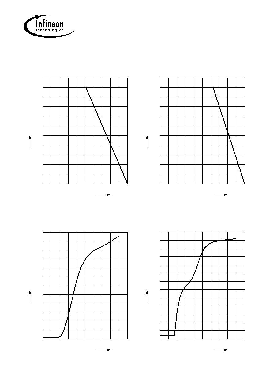
Total power dissipation P
tot
=
(T
S
)
BF1005, BF1005R
0
15
30
45
60
75
90 105 120 ∞C
150
T
S
0
20
40
60
80
100
120
140
160
180
mW
220
P
tot
Total power dissipation P
tot
=
(T
S
)
BF1005W
0
15
30
45
60
75
90 105 120 ∞C
150
T
S
0
20
40
60
80
100
120
140
160
180
mA
220
P
tot
Drain current I
D
=
(V
G2S
)
0
0.5
1
1.5
2
2.5
3
3.5
4
V
5
V
G2S
0
1
2
3
4
5
6
7
8
9
10
mA
12
I
D
Insertion power gain
|S
21
|≤ =
(V
G2S
)
0
0.5
1
1.5
2
2.5
3
3.5
4
V
5
V
G2S
-55
-50
-45
-40
-35
-30
-25
-20
-15
-10
-5
0
dB
10
|
S
21
|≤
Feb-18-2004
5
BF1005...
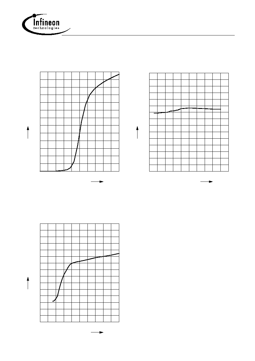
Forward transfer admittance
|Y
21
| =
(V
G2S
)
0
0.5
1
1.5
2
2.5
3
3.5
4
V
5
V
G2S
0
2
4
6
8
10
12
14
16
18
20
22
mS
26
|
Y
21
|
Gate 1 input capacitance C
g1ss
=
(V
g2s
)
f = 200MHz
0.5
1
1.5
2
2.5
3
3.5
4
4.5 V
5.5
V
G2S
0
0.2
0.4
0.6
0.8
1
1.2
1.4
1.6
1.8
2
2.2
2.4
pF
3
C
g1ss
Output capacitance C
dss
=
(V
G2S
)
f = 200MHz
0
0.5
1
1.5
2
2.5
3
3.5
4
V
5
V
G2S
0
0.2
0.4
0.6
0.8
1
1.2
1.4
1.6
1.8
2
2.2
2.4
pF
3
C
dss