
BFP196W
Jun-22-2001
1
NPN Silicon RF Transistor
For low noise, low distortion broadband
amplifiers in antenna and telecommunications
systems up to 1.5 GHz at collector currents from
20 mA to 89 mA
Power amplifier for DECT and PCN systems
f
T
= 7.5 GHz
F = 1.5 dB at 900 MHz
VPS05605
4
2
1
3
ESD
: Electrostatic discharge sensitive device, observe handling precaution!
Type
Marking
Pin Configuration
Package
BFP196W
RIs
1 = E
2 = C
3 = E
4 = B
SOT343
Maximum Ratings
Parameter
Symbol
Value
Unit
Collector-emitter voltage
V
CEO
12
V
Collector-emitter voltage
V
CES
20
Collector-base voltage
V
CBO
20
Emitter-base voltage
V
EBO
2
Collector current
I
C
100
mA
Base current
I
B
12
Total power dissipation
T
S
69 �C
1)
P
tot
700
mW
Junction temperature
T
j
150
�C
Ambient temperature
T
A
-65 ... 150
Storage temperature
T
stg
-65 ... 150
Thermal Resistance
Junction - soldering point
2)
R
thJS
115
K/W
1T
S
is measured on the collector lead at the soldering point to the pcb
2For calculation of R
thJA
please refer to Application Note Thermal Resistance

BFP196W
Jun-22-2001
2
Electrical Characteristics at T
A
= 25�C, unless otherwise specified.
Parameter
Values
Unit
Symbol
min.
max.
typ.
DC characteristics
V
V
(BR)CEO
Collector-emitter breakdown voltage
I
C
= 1 mA, I
B
= 0
12
-
-
�A
Collector-emitter cutoff current
V
CE
= 20 V, V
BE
= 0
-
100
-
I
CES
Collector-base cutoff current
V
CB
= 10 V, I
E
= 0
I
CBO
-
-
100
nA
Emitter-base cutoff current
V
EB
= 1 V, I
C
= 0
I
EBO
-
-
1
�A
DC current gain
I
C
= 50 mA, V
CE
= 8 V
h
FE
50
100
200
-

BFP196W
Jun-22-2001
3
Electrical Characteristics at T
A
= 25�C, unless otherwise specified.
Parameter
Symbol
Values
Unit
min.
typ.
max.
AC characteristics
(verified by random sampling)
Transition frequency
I
C
= 70 mA, V
CE
= 8 V, f = 500 MHz
f
T
5
7.5
-
GHz
Collector-base capacitance
V
CB
= 10 V, f = 1 MHz
C
cb
-
1
1.4
pF
Collector-emitter capacitance
V
CE
= 10 V, f = 1 MHz
C
ce
-
0.36
-
Emitter-base capacitance
V
EB
= 0.5 V, f = 1 MHz
C
eb
-
3.7
-
Noise figure
I
C
= 20 mA, V
CE
= 8 V, Z
S
= Z
Sopt
,
f
= 900 MHz
f
= 1.8 GHz
F
-
-
1.5
2.5
-
-
dB
Power gain, maximum available
1)
I
C
= 50 mA, V
CE
= 8 V, Z
S
= Z
Sopt
, Z
L
= Z
Lopt
,
f
= 900 MHz
f
= 1.8 GHz
G
ma
-
-
17.5
11.5
-
-
Transducer gain
I
C
= 50 mA, V
CE
= 8 V, Z
S
= Z
L
= 50
,
f
= 900 MHz
f
= 1.8 GHz
|S
21e
|
2
-
-
12.5
6.5
-
-
1
G
ma
= |S
21
/ S
12
| (k-(k
2
-1)
1/2
)

BFP196W
Jun-22-2001
4
SPICE Parameters (Gummel-Poon Model, Berkley-SPICE 2G.6 Syntax) :
Transistor Chip Data
BF =
125
-
IKF =
0.4294
A
BR =
-
10.584
IKR =
0.019511
A
RB =
1.2907
RE =
0.75103
VJE =
0.7308
V
XTF =
0.44322
-
PTF =
0
deg
MJC =
0.3289
-
CJS =
0
fF
XTB =
0
-
FC =
0.50922
-
IS =
1.7264
fA
VAF =
20
V
NE =
1.1766
-
VAR =
V
3.8128
NC =
0.88299
-
RBM =
1
CJE =
13.325
fF
TF =
ps
23.994
ITF =
1.9775
mA
VJC =
0.73057
V
TR =
ns
2.2413
MJS =
0
-
XTI =
3
-
NF =
0.80012
-
ISE =
119.22
fA
NR =
0.94288
-
ISC =
4.8666
fA
IRB =
0.084011
mA
RC =
0.27137
MJE =
0.33018
-
VTF =
0.1
V
CJC =
1667
fF
XCJC =
0.29998
-
VJS =
0.75
V
EG =
1.11
eV
TNOM
300
K
All parameters are ready to use, no scalling is necessary.
Extracted on behalf of Infineon Technologies AG by:
Institut f�r Mobil-und Satellitentechnik (IMST)
Package Equivalent Circuit:
L
BI
=
0.43
nH
L
BO
=
0.47
nH
L
EI
=
0.26
nH
L
EO
=
0.12
nH
L
CI
=
0.06
nH
L
CO
=
0.36
nH
C
BE
=
68
fF
C
CB
=
46
fF
C
CE
=
232
fF
Valid up to 6GHz
For examples and ready to use parameters please contact your local Infineon Technologies distributor or sales
office to obtain a Infineon Technologies CD-ROM or see Internet: http://www.infineon.com/products/discrete/index.htm
BFP196W
Jun-22-2001
5
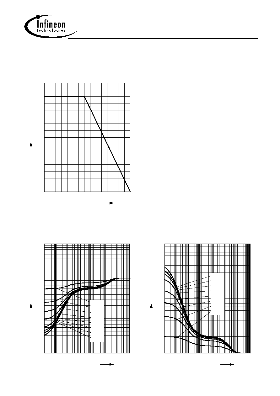
Total power dissipation P
tot
= f (T
S
)
0
20
40
60
80
100
120 �C
150
T
S
0
100
200
300
400
500
600
mW
800
P
tot
Permissible Pulse Load R
thJS
= f (t
p
)
10
-7
10
-6
10
-5
10
-4
10
-3
10
-2
10
0
s
t
p
0
10
1
10
2
10
3
10
K/W
R
thJS
0.5
0.2
0.1
0.05
0.02
0.01
0.005
D = 0
Permissible Pulse Load
P
totmax
/P
totDC
= f (t
p
)
10
-7
10
-6
10
-5
10
-4
10
-3
10
-2
10
0
s
t
p
0
10
1
10
2
10
-
P
tot
m
ax
/ P
totDC
D = 0
0.005
0.01
0.02
0.05
0.1
0.2
0.5
BFP196W
Jun-22-2001
6
Collector-base capacitance C
cb
= f (V
CB
)
f = 1MHz
0
4
8
12
16
V
22
V
CB
0.0
0.2
0.4
0.6
0.8
1.0
1.2
1.4
1.6
pF
2.0
C
cb
Transition frequency f
T
= f (I
C
)
V
CE
= Parameter
0
20
40
60
80
mA
120
I
C
0.0
0.5
1.0
1.5
2.0
2.5
3.0
3.5
4.0
4.5
5.0
5.5
6.0
GHz
7.5
f
T
10V
5V
3V
2V
1V
0.7V
Power Gain G
ma
, G
ms
= f(I
C
)
f = 0.9GHz
V
CE
= Parameter
0
20
40
60
80
mA
120
I
C
8
9
10
11
12
13
14
15
16
17
18
dB
20
G
8V
3V
2V
1V
0.7V
Power Gain G
ma
, G
ms
= f(I
C
)
f = 1.8GHz
V
CE
= Parameter
0
20
40
60
80
mA
120
I
C
4
5
6
7
8
9
10
dB
12
G
8V
3V
2V
1V
0.7V

BFP196W
Jun-22-2001
7
Intermodulation Intercept Point IP
3
=f(I
C
)
(3rd order, Output,
Z
S
=Z
L
=50
)
V
CE
= Parameter, f = 900MHz
0
20
40
60
80
mA
120
I
C
14
16
18
20
22
24
26
28
30
32
34
dBm
38
IP
3
8V
5V
3V
2V
1V
Power Gain G
ma
, G
ms
= f(V
CE
):_____
|S
21
|
2
= f(V
CE
):---------
f = Parameter
0
1
2
3
4
5
6
7
8
V
10
V
CE
0
2
4
6
8
10
12
14
dB
18
G
0.9GHz
1.8GHz
0.9GHz
1.8GHz
I
C
=50mA
Power Gain |S
21
|
2
= f(f)
V
CE
=
Parameter
0.0
0.5
1.0
1.5
2.0
2.5
GHz
3.5
f
-4
0
4
8
12
16
20
24
dB
32
S
21
8V
1V
0.7V
I
C
=50mA
Power Gain G
ma
, G
ms
= f(f)
V
CE
= Parameter
0.0
0.5
1.0
1.5
2.0
2.5
GHz
3.5
f
4
6
8
10
12
14
16
18
20
22
24
26
28
dB
32
G
8V
1V
0.7V
I
C
=50mA