2003-10-29
Page 1
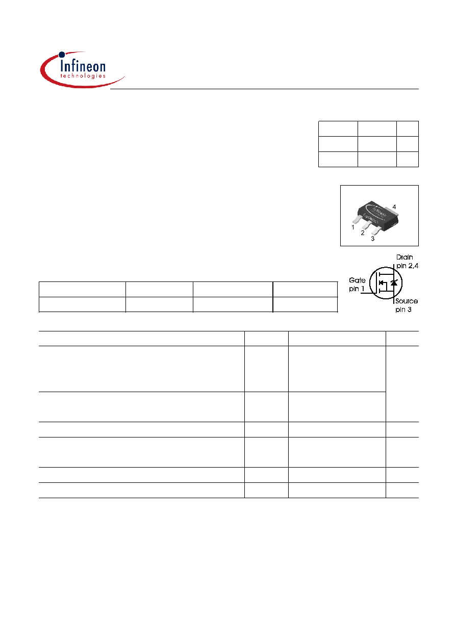
BSP615S2L
Opti
MOS
Power-Transistor
Product Summary
V
DS
55
V
R
DS(on)
90
m
I
D
2.8
A
Feature
·
N-Channel
·
Enhancement mode
·
Logic Level
SOT 223
Marking
2N615L
Type
Package
Ordering Code
BSP615S2L
SOT 223
Q67060-S7211
Maximum Ratings, at T
j
= 25 °C, unless otherwise specified
Parameter
Symbol
Value
Unit
Continuous drain current
T
A
=25°C
T
A
=70°C
I
D
2.8
2.3
A
Pulsed drain current
T
A
=25°C
I
D puls
11
Gate source voltage
V
GS
± 20
V
Power dissipation
T
A
=25°C
P
tot
1.8
W
Operating and storage temperature
T
j ,
T
stg
-55... +150
°C
IEC climatic category; DIN IEC 68-1
55/150/00
2003-10-29
Page 2
BSP615S2L
Thermal Characteristics
Parameter
Symbol
Values
Unit
min.
typ.
max.
Characteristics
Thermal resistance, junction - soldering point
(Pin 4)
R
thJS
-
19
23
K/W
Thermal resistance, chip to ambient air:
@ min. footprint
@ 6 cm
2
cooling area
1)
R
thJA
-
-
-
-
120
70
Electrical Characteristics, at T
j
= 25 °C, unless otherwise specified
Parameter
Symbol
Values
Unit
min.
typ.
max.
Static Characteristics
Drain-source breakdown voltage
V
GS
=0V,
I
D
=1mA
V
(BR)DSS
55
-
-
V
Gate threshold voltage, V
GS
= V
DS
I
D
=12µA
V
GS(th)
1.2
1.6
2
Zero gate voltage drain current
V
DS
=55V,
V
GS
=0V,
T
j
=25°C
V
DS
=55V,
V
GS
=0V,
T
j
=125°C
2)
I
DSS
-
-
0.1
10
1
100
µA
Gate-source leakage current
V
GS
=20V,
V
DS
=0V
I
GSS
-
10
100
nA
Drain-source on-state resistance
V
GS
=4.5V,
I
D
=1.4A
R
DS(on)
-
86
150
m
Drain-source on-state resistance
V
GS
=10V,
I
D
=1.4A
R
DS(on)
-
67
90
1Device on 40mm*40mm*1.5mm epoxy PCB FR4 with 6cm² (one layer, 70 µm thick) copper area for drain
connection. PCB is vertical without blown air.
2Defined by design. Not subject to production test.
2003-10-29
Page 3
BSP615S2L
Electrical Characteristics
Parameter
Symbol
Conditions
Values
Unit
min.
typ.
max.
Dynamic Characteristics
Transconductance
g
fs
V
DS
2*I
D
*R
DS(on)max
,
I
D
=2.3A
2.7
5.4
-
S
Input capacitance
C
iss
V
GS
=0V, V
DS
=25V,
f=1MHz
-
249
330 pF
Output capacitance
C
oss
-
58
78
Reverse transfer capacitance
C
rss
-
22
33
Turn-on delay time
t
d(on)
V
DD
=30V, V
GS
=4.5V,
I
D
=2.8A,
R
G
=24
-
7.8
12
ns
Rise time
t
r
-
24
36
Turn-off delay time
t
d(off)
-
22
33
Fall time
t
f
-
23
34
Gate Charge Characteristics
Gate to source charge
Q
gs
V
DD
=40V, I
D
=2.8A
-
0.8
1.1
nC
Gate to drain charge
Q
gd
-
2.5
3.8
Gate charge total
Q
g
V
DD
=40V, I
D
=2.8A,
V
GS
=0 to 10V
-
7.5
10
Gate plateau voltage
V
(plateau) V
DD
=40V, I
D
=2.8A
-
3
-
V
Reverse Diode
Inverse diode continuous
forward current
I
S
T
A
=25°C
-
-
2.8
A
Inv. diode direct current, pulsed
I
SM
-
-
11
Inverse diode forward voltage
V
SD
V
GS
=0V, I
F
=2.8A
-
0.8
1.1
V
Reverse recovery time
t
rr
V
R
=30V, I
F=
l
S
,
di
F
/dt=100A/µs
-
30
38
ns
Reverse recovery charge
Q
rr
-
30
38
nC
2003-10-29
Page 5
BSP615S2L
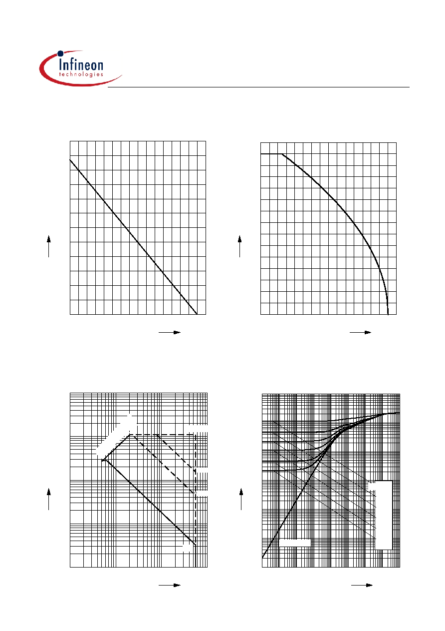
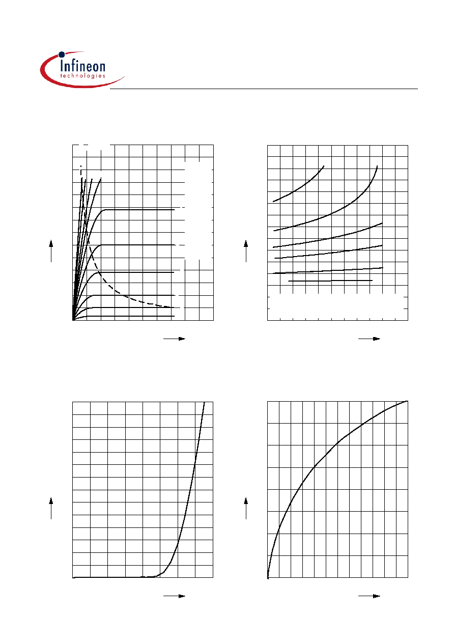
5 Typ. output characteristic
I
D
= f (V
DS
); T
j
=25°C
parameter: t
p
= 80 µs
0
0.5
1
1.5
2
2.5
3
3.5
4
V
5
V
DS
0
0.5
1
1.5
2
2.5
3
3.5
4
4.5
5
5.5
6
A
7
BSP615S2L
I
D
VGS [V]
a
a
2.6
b
b
2.8
c
c
3.0
d
d
3.2
e
e
3.4
f
f
3.6
g
g
3.8
h
h
4.0
i
i
4.5
j
P
tot
= 1.8W
j
10.0
6 Typ. drain-source on resistance
R
DS(on)
= f (I
D
)
parameter: V
GS
0
1
2
3
4
A
5.5
I
D
0
20
40
60
80
100
120
140
160
180
200
220
240
m
300
BSP615S2L
R
DS(on)
V
GS
[V] =
e
e
3.4
f
f
3.6
g
g
3.8
h
h
4.0
i
i
4.5
j
j
10.0
7 Typ. transfer characteristics
I
D
= f ( V
GS
); V
DS
2 x I
D
x R
DS(on)max
parameter: t
p
= 80 µs
0
0.5
1
1.5
2
2.5
3
V
4
V
GS
0
0.4
0.8
1.2
1.6
2
2.4
2.8
3.2
3.6
4
4.4
4.8
A
5.6
I
D
8 Typ. forward transconductance
g
fs
= f(I
D
); T
j
=25°C
parameter: g
fs
0
1
2
3
4
A
6
I
D
0
1
2
3
4
5
6
S
8
g
fs