 | –≠–ª–µ–∫—Ç—Ä–æ–Ω–Ω—ã–π –∫–æ–º–ø–æ–Ω–µ–Ω—Ç: BSP77 | –°–∫–∞—á–∞—Ç—å:  PDF PDF  ZIP ZIP |

2004-03-05
Page 1
HITFET
“
II.Generation BSP 77
Smart Lowside Power Switch
Product Summary
Drain source voltage
V
DS
42
V
On-state resistance
R
DS(on)
100
m
W
Nominal load current
I
D(Nom)
2.17
A
Clamping energy
E
AS
250
mJ
Features
∑ Logic Level Input
∑ Input Protection (ESD)
∑ Thermal shutdown with
auto restart
∑ Overload protection
∑ Short circuit protection
∑ Overvoltage protection
∑ Current limitation
∑ Analog driving possible
VPS05163
1
2
3
4
Application
∑ All kinds of resistive, inductive and capacitive loads in switching
or linear applications
∑ µC compatible power switch for 12 V DC applications
∑ Replaces electromechanical relays and discrete circuits
General Description
N channel vertical power FET in Smart SIPMOS“ technology. Fully protected by embedded
protection functions.
Gate-Driving
Unit
ESD
Overload
Protection
Over-
temperature
Protection
Short circuit
Protection
Overvoltage-
Protection
Current
Limitation
M
V
bb
In
Source
Drain
HITFET
‚
Pin 1
Pin 2 and 4 (TAB)
Pin 3
Complete product spectrum and additional information http://www.infineon.com/hitfet

2004-03-05
Page 2
BSP 77
Maximum Ratings at T
j
= 25∞C, unless otherwise specified
Parameter
Symbol
Value
Unit
Drain source voltage
V
DS
42
V
Supply voltage for full short circuit protection
V
bb(SC)
42
Continuous input voltage
1)
V
IN
-0.2
2)
... +10
Continuous input current
2)
-0.2V
£ V
IN
£ 10V
V
IN
< -0.2V or V
IN
> 10V
I
IN
self limited
| I
IN
|
£ 2
mA
Operating temperature
T
j
-40 ...+150
∞C
Storage temperature
T
stg
-55 ... +150
Power dissipation
5)
T
C
= 85 ∞C
P
tot
3.8
W
Unclamped single pulse inductive energy
2)
E
AS
250
mJ
Load dump protection V
LoadDump
2)3)
= V
A
+ V
S
V
IN
= 0 and 10 V, t
d
= 400 ms, R
I
= 2
W,
R
L
= 6
W, V
A
= 13.5 V
V
LD
50
V
Electrostatic discharge voltage
2)
(Human Body Model)
according to Jedec norm
EIA/JESD22-A114-B, Section 4
V
ESD
2
kV
Jedec humidity category,J-STD-20-B
MSL 1
IEC climatic category; DIN EN 60068-1
40/150/56
Thermal resistance
junction - ambient:
@ min. footprint
@ 6 cm
2
cooling area
4)
R
thJA
125
72
K/W
junction-soldering point:
R
thJS
17
K/W
1For input voltages beyond these limits I
IN
has to be limited.
2not subject to production test, specified by design
3VLoaddump is setup without the DUT connected to the generator per ISO 7637-1 and DIN 40839
4 Device on 50mm*50mm*1.5mm epoxy PCB FR4 with 6cm2 (one layer, 70µm thick) copper area for drain
connection. PCB mounted vertical without blown air.
5not subject to production test, calculated by RthJA and Rds(on)

2004-03-05
Page 3
BSP 77
Electrical Characteristics
Parameter
Symbol
Values
Unit
at T
j
= 25∞C, unless otherwise specified
min.
typ.
max.
Characteristics
Drain source clamp voltage
T
j
= - 40 ...+ 150 ∞C, I
D
= 10 mA
V
DS(AZ)
42
-
55
V
Off-state drain current
T
J
= -40...+85 ∞C, V
DS
= 32 V, V
IN
= 0 V
T
j
= 150 ∞C
I
DSS
-
-
1.5
4
8
12
µA
Input threshold voltage
I
D
= 0.
6 mA, T
j
= 25 ∞C
I
D
= 0.
6 mA, T
j
= 150 ∞C
V
IN(th)
1.3
0.8
1.7
-
2.2
-
V
On state input current
I
IN(on)
-
10
30
µA
On-state resistance
V
IN
= 5 V, I
D
= 2.17 A, T
j
= 25 ∞C
V
IN
= 5 V, I
D
= 2.17 A, T
j
= 150 ∞C
R
DS(on)
-
-
90
160
120
240
m
W
On-state resistance
V
IN
= 10 V, I
D
= 2.17 A, T
j
= 25 ∞C
V
IN
= 10 V, I
D
= 2.17 A, T
j
= 150 ∞C
R
DS(on)
-
-
70
130
100
200
Nominal load current
5)
V
DS
= 0.5 V, T
j
< 150∞C, V
IN
= 10 V, T
A
= 85 ∞C
I
D(Nom)
2.17
2.8
-
A
Current limit (active if V
DS
>2.5 V)
1)
V
IN
= 10 V, V
DS
= 12 V, t
m
= 200 µs
I
D(lim)
10
15
20
1Device switched on into existing short circuit (see diagram Determination of ID(lim)). If the device is in on condition
and a short circuit occurs, these values might be exceeded for max. 50 µs.
5not subject to production test, calculated by RthJA and Rds(on)

2004-03-05
Page 4
BSP 77
Electrical Characteristics
Parameter
Symbol
Values
Unit
at T
j
= 25∞C, unless otherwise specified
min.
typ.
max.
Dynamic Characteristics
Turn-on time V
IN
to 90% I
D
:
R
L
= 4.7
W, V
IN
= 0 to 10 V, V
bb
= 12 V
t
on
-
40
100
µs
Turn-off time V
IN
to 10% I
D
:
R
L
= 4.7
W, V
IN
= 10 to 0 V, V
bb
= 12 V
t
off
-
70
100
Slew rate on 70 to 50% V
bb
:
R
L
= 4.7
W, V
IN
= 0 to 10 V, V
bb
= 12 V
-dV
DS
/dt
on
-
0.4
1.5
V/µs
Slew rate off 50 to 70% V
bb
:
R
L
= 4.7
W, V
IN
= 10 to 0 V, V
bb
= 12 V
dV
DS
/dt
off
-
0.6
1.5
Protection Functions
1)
Thermal overload trip temperature
T
jt
150
175
-
∞C
Thermal hysteresis
2)
DT
jt
-
10
-
K
Input current protection mode
T
j
= 150 ∞C
I
IN(Prot)
-
100
300
µA
Unclamped single pulse inductive energy
2)
I
D
= 2.17 A, T
j
= 25 ∞C, V
bb
= 12 V
E
AS
250
-
-
mJ
Inverse Diode
Inverse diode forward voltage
I
F
= 10.9 A, t
m
= 250 µs, V
IN
= 0 V,
t
P
= 300 µs
V
SD
-
1
1.5
V
1Integrated protection functions are designed to prevent IC destruction under fault conditions
described in the data sheet. Fault conditions are considered as "outside" normal operating range.
Protection functions are not designed for continuous repetitive operation.
2not subject to production test, specified by design
2004-03-05
Page 5
BSP 77
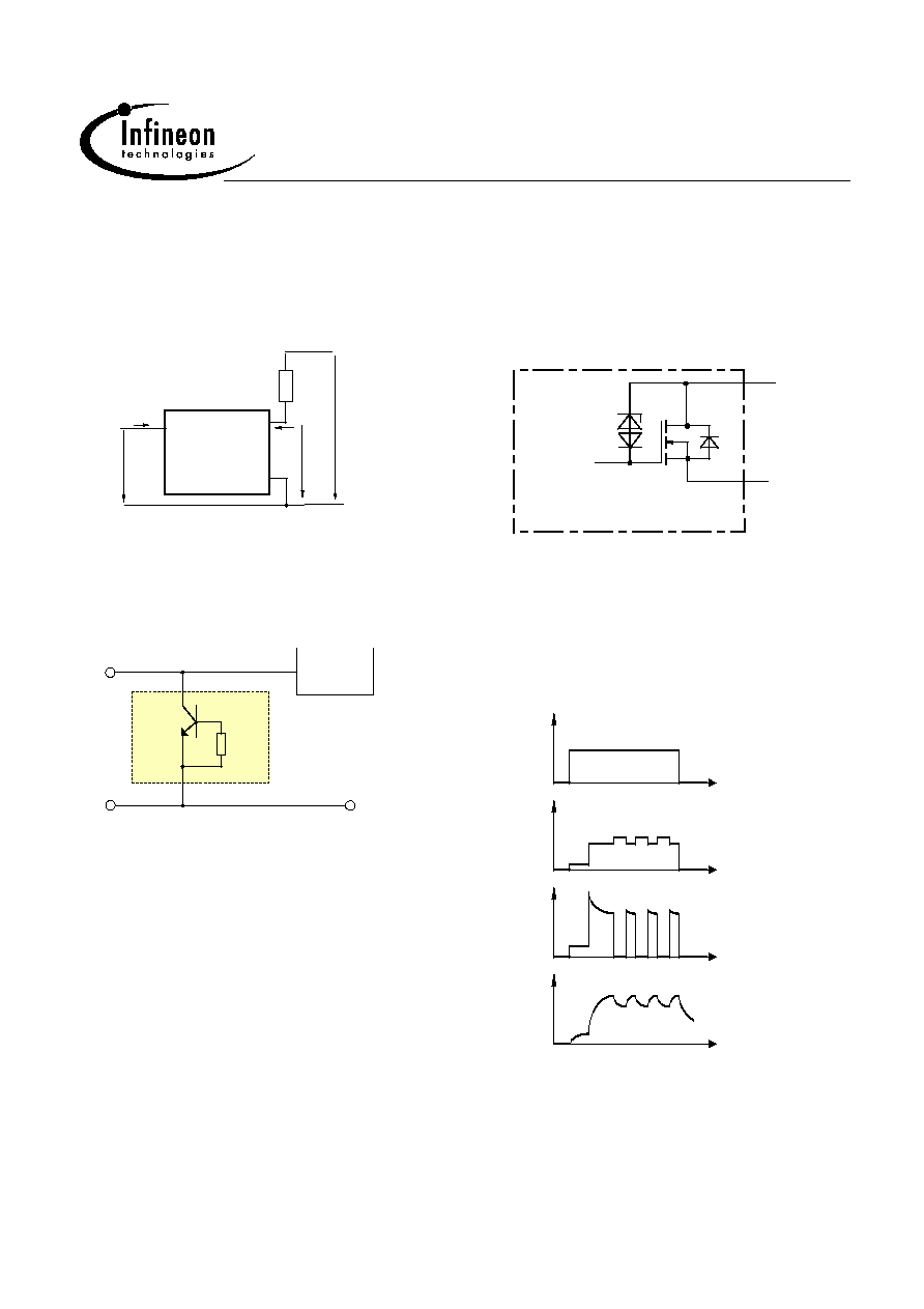
Block diagram
Inductive and overvoltage
output clamp
Terms
HITFET
IN
D
VIN
ID
VDS
1
IIN
S
Vbb
RL
2
3
HITFET
VZ
D
S
Short circuit behaviour
Input circuit (ESD protection)
Gate Drive
Source/
Ground
Input
V
IN
I
IN
I
DS
T
j

2004-03-05
Page 6
BSP 77
1 Maximum allowable power dissipation
P
tot
= f(T
S
) resp.
P
tot
= f(T
A
) @ R
thJA
=72 K/W
-75
-50
-25
0
25
50
75
100 ∞C
150
T
S
;T
A
0
1
2
3
4
5
6
7
8
W
10
P
tot
6cm2
max.
2 On-state resistance
R
ON
= f(T
j
); I
D
=2.17A; V
IN
=10V
-50
-25
0
25
50
75
100 125 ∞C
175
T
j
0
25
50
75
100
125
150
175
m
W
225
R
DS(on)
typ.
max.
3 On-state resistance
R
ON
= f(T
j
); I
D
= 2.17A; V
IN
=5V
-50
-25
0
25
50
75
100 125 ∞C
175
T
j
0
25
50
75
100
125
150
175
200
m
W
250
R
DS(on)
typ.
max.
4 Typ. input threshold voltage
V
IN(th)
= f(T
j
); I
D
= 0.3 mA; V
DS
= 12V
-50
-25
0
25
50
75
100
∞C
150
T
j
0
0.2
0.4
0.6
0.8
1
1.2
1.4
1.6
V
2
V
GS(th)

2004-03-05
Page 7
BSP 77
5 Typ. transfer characteristics
I
D
=f(V
IN
); V
DS
=12V; T
Jstart
=25∞C
1
2
3
4
5
6
7
8
V
10
V
IN
0
2
4
6
8
10
12
A
16
I
D
6 Typ. short circuit current
I
D(lim)
= f(T
j
); V
DS
=12V
Parameter: V
IN
-50
-25
0
25
50
75
100 125 ∞C
175
T
j
10
12
14
16
18
20
A
24
I
D
5V
Vin=10V
7 Typ. output characteristics
I
D
=f(V
DS
); T
Jstart
=25∞C
Parameter: V
IN
0
1
2
3
4
V
6
V
DS
0
2
4
6
8
10
12
14
16
A
20
I
D
3V
4V
5V
6V
7V
Vin=10V
8 Off-state drain current
I
DSS
= f(T
j
)
-50
-25
0
25
50
75
100 125 ∞C
175
T
j
0
1
2
3
4
5
6
7
8
9
10
11
µA
13
I
DSS
typ.
max.

2004-03-05
Page 8
BSP 77
9 Typ. overload current
I
D(lim)
= f(t), V
bb
=12 V, no heatsink
Parameter: T
jstart
0
1
2
3
ms
5
t
0
5
10
15
A
25
I
D(lim)
-40∞C
25∞C
85∞C
+150∞C
10 Typ. transient thermal impedance
Z
thJA
=f(t
p
) @ 6 cm
2
cooling area
Parameter: D=t
p
/T
10
-7
10
-6
10
-5
10
-4
10
-3
10
-2
10
-1
10
0
10
1
10
3
s
t
p
-2
10
-1
10
0
10
1
10
2
10
K/W
Z
thJA
Single pulse
0.01
0.02
0.05
0.1
0.2
D=0.5
11 Determination of I
D(lim)
I
D(lim)
= f(t); t
m
= 200µs
Parameter: T
Jstart
0
0.1
0.2
0.3
0.4
ms
0.6
t
0
5
10
15
A
25
I
D(lim)
-40∞C
25∞C
85∞C
150∞C

2004-03-05
Page 9
BSP 77
Package
Ordering Code
SOT-223
Q67060-S7202-A3
±0.1
±0.2
±0.1
0.7
4
3
2
1
GPS05560
6.5
3
acc. to
+0.2
DIN 6784
1.6
±0.1
15∞ max
±0.04
0.28
7
±0.3
±0.2
3.5
0.5
0.1 max
min
B
M
0.25
B
A
2.3
4.6
A
M
0.25

Page 10
2004-03-05
BSP 7
7
Revision History :
2004-03-05
Previous version :
2003-04-22
For questions on technology, delivery and prices please contact the Infineon Technologies Offices in Germany
or the Infineon Technologies Companies and Representatives worldwide: see our webpage at
http://www.infineon.com
HITFET
Æ
, SIPMOS
Æ
are registered trademarks of Infineon Technologies AG.
Edition 2004-02-02
Published by Infineon Technologies AG,
St.-Martin-Strasse 53,
D-81541 M¸nchen, Germany
© Infineon Technologies AG 2001
All Rights Reserved.
Attention please!
The information herein is given to describe certain components and shall not be considered as a guarantee
of characteristics.
Terms of delivery and rights to technical change reserved.
We hereby disclaim any and all warranties, including but not limited to warranties of non-infringement,
regarding circuits, descriptions and charts stated herein.
Infineon Technologies is an approved CECC manufacturer.
Information
For further information on technology, delivery terms and conditions and prices please contact your
nearest Infineon Technologies Office in Germany or our Infineon Technologies Representatives worldwide
(see address list).
Warnings
Due to technical requirements components may contain dangerous substances. For information on the
types in question please contact your nearest Infineon Technologies Office.
Infineon Technologies Components may only be used in life-support devices or systems with the express
written approval of Infineon Technologies, if a failure of such components can reasonably be expected to
cause the failure of that life-support device or system, or to affect the safety or effectiveness of that device
or system. Life support devices or systems are intended to be implanted in the human body, or to support
and/or maintain and sustain and/or protect human life. If they fail, it is reasonable to assume that the health
of the user or other persons may be endangered.
Page
Subjects (major changes since last revision)
2, 4
Footnote 2 extended to Vin<0V, E
tot
and
T
jT
2, 3
Footnote 5 implemented to P
tot
and I
D(nom)
2
ESD test condition changed from MIL STD 883D, methode 3015.7 and EOS/ESD assn.
standard S5.1-1993 to Jedec Norm EIA/JESD22-A114-B, Section 4
2
Humidity category classification changed from DIN 40040 value E to J-STD-20-B value MSL1
2
Climatic category changed from DIN IEC 68-1 to DIN EN 60068-1
3
V
IN(th)
test conditions from I
D
=0.
3mA to I
D
=0.
6mA