 | –≠–ª–µ–∫—Ç—Ä–æ–Ω–Ω—ã–π –∫–æ–º–ø–æ–Ω–µ–Ω—Ç: BTS333 | –°–∫–∞—á–∞—Ç—å:  PDF PDF  ZIP ZIP |
Nov-03-2000
Page 1
HITFET
BTS 333
Smart Lowside Power Switch
Features
∑ Logic Level Input
∑ Input Protection (ESD)
∑ Temperature limitation
adjustable by input voltage
∑ Overload protection
∑ Short circuit protection
∑ Overvoltage protection
∑
Current limitation
∑ Analog driving possible
Product Summary
Drain source voltage
V
DS
42
V
On-state resistance
R
DS(on)
18
m
Nominal load current
I
D(ISO)
19
A
Clamping energy
E
AS
2
J
Application
∑ All kinds of resistive, inductive and capacitive loads in switching or linear
applications
∑ µC compatible power switch for 12 V and 24 V DC applications
∑ Replaces electromechanical relays and discrete circuits
General Description
N channel vertical power FET in Smart SIPMOS technology. Fully protected by embedded
protection functions.
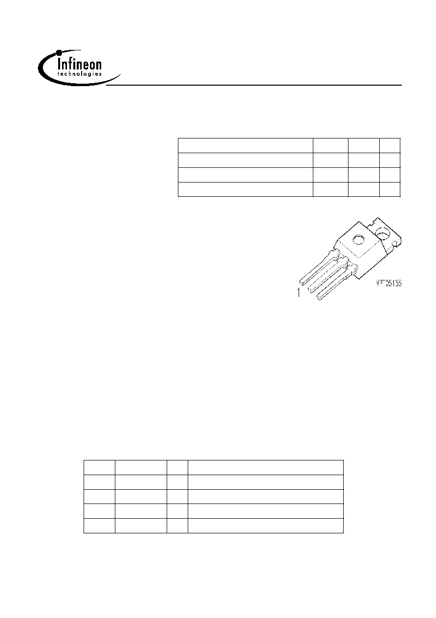
Pin
Symbol
Function
1
IN
Input
2
DRAIN
Output to the load
3
SOURCE
Ground
TAB
DRAIN
Output to the load
Nov-03-2000
Page 2
BTS 333
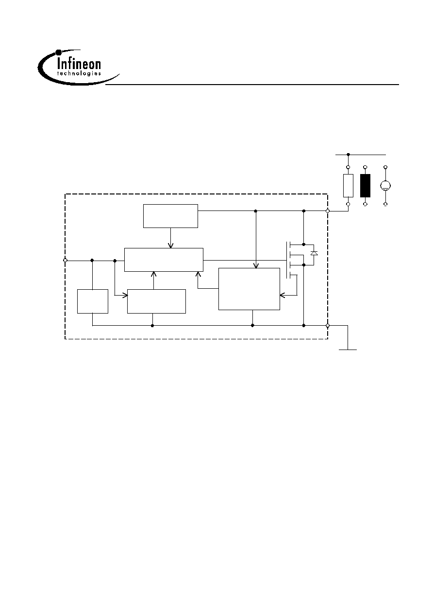
Block Diagram
Gate-Control
ESD
Temperature
Control
Current
limitation +
Short circuit
Protection
Overvoltage-
Protection
M
V
bb
In
Source
Drain
BTS333
Pin 1
Pin 2 and TAB
Pin 3

Nov-03-2000
Page 3
BTS 333
Maximum Ratings at T
j
= 25∞C, unless otherwise specified
Parameter
Symbol
Value
Unit
Drain source voltage
V
DS
42
V
Drain source voltage for full SCP
SCP Type I, V
IN
10V
SCP Type II, V
IN
7V
V
DS(SC)
36
24
Continuous input current
-0.2V
V
IN
10V
V
IN
< -0.2V or V
IN
> 10V
I
IN
no limit
| I
IN
|
4
mA
Operating temperature
1)
T
j
-40 ...+175
∞C
Storage temperature
T
stg
-55 ... +150
Power dissipation
T
C
= 85 ∞C
P
tot
100
W
Unclamped single pulse inductive energy
2)
I
D
= 19 A, T
j
= 25 ∞C, V
bb
= 12 V
I
D
= 19 A, T
j
= 150 ∞C, V
bb
= 12 V
E
AS
2
0.5
J
Load dump protection V
LoadDump
3)
= V
A
+ V
S
V
IN
= 0 and 10 V, t
d
= 400 ms, R
I
= 2
,
R
L
= 1
, V
A
= 13.5 V
V
LD
55
V
E
lectrostatic discharge voltage
(Human Body Model)
according to MIL STD 883D, method 3015.7 and
EOS/ESD assn. standard S5.1 - 1993
V
ESD
2
kV
DIN humidity category, DIN 40 040
E
IEC climatic category; DIN IEC 68-1
40/150/56
Thermal resistance
junction - case:
R
thJC
0.8
K/W
junction - case:
R
thJA
75
1Temperatures above 175∞C will reduce lifetime of the device
2 Not tested, specified by design.
3VLoaddump is setup without the DUT connected to the generator per ISO 7637-1 and DIN 408

Nov-03-2000
Page 4
BTS 333
Electrical Characteristics
Parameter
Symbol
Values
Unit
at T
j
= 25∞C, unless otherwise specified
min.
typ.
max.
Characteristics
Drain source clamp voltage
T
j
= - 40 ...+ 150, I
D
= 10 mA
V
DS(AZ)
42
-
55
V
Off-state drain current
V
DS
= 32 V, T
j
=-40 ... +85∞C , V
IN
= 0 V
V
DS
= 32 V, T
j
=-40 ... +150∞C , V
IN
= 0 V
I
DSS
-
-
1
1
5
20
µA
Gate threshold voltage, V
GS
= V
DS
I
D
= 1.9 mA, T
j
= -40 ∞C
I
D
= 1.9 mA, T
j
= 25 ∞C
V
GS(th)
-
1.3
-
1.7
2.4
2.2
V
On state input current (temp. limit. inactiv)
V
IN
= 10 V
V
IN
= 5 V
I
IN(on)
-
-
200
10
300
30
µA
On-state resistance
V
IN
= 5 V, I
D
= 19 A, T
j
= 25 ∞C
V
IN
= 5 V, I
D
= 19 A, T
j
= 150 ∞C
R
DS(on)
-
-
18
29
23
46
m
On-state resistance
V
IN
= 10 V, I
D
= 19 A, T
j
= 25 ∞C
V
IN
= 10 V, I
D
= 19 A, T
j
= 150 ∞C
R
DS(on)
-
-
14
26
18
36
Nominal load current
V
IN
= 10 V, T
j
< 150∞C, T
A
= 85 ∞C
I
D(ISO)
19
-
-
A
Continuous drain current
1)
T
C
= 120 ∞C, V
IN
= 10 V
I
D
25
-
-
Current limit (active if V
DS
>2.5 V)
2)
V
IN
= 10 V, V
DS
= 12 V, t
m
= 300 µs
I
D(lim)
35
50
65
1if not limited by current limitation
2Device switched on into existing short circuit (see diagram Determination of ID(lim)). If the device is in on condition
and a short circuit occurs, these values might be exceeded for max. 50 µs.

Nov-03-2000
Page 5
BTS 333
Electrical Characteristics
Parameter
Symbol
Values
Unit
at T
j
= 25∞C, unless otherwise specified
min.
typ.
max.
Dynamic Characteristics
Turn-on time V
IN
to 90% I
D
:
R
L
= 2
, V
IN
= 0 to 10 V, V
bb
= 12 V
t
on
-
140
250
µs
Turn-off time V
IN
to 10% I
D
:
R
L
= 2
, V
IN
= 10 to 0 V, V
bb
= 12 V
t
off
-
250
350
Slew rate on 70 to 50% V
bb
:
R
L
= 2
, V
IN
= 0 to 10 V, V
bb
= 12 V
-dV
DS
/dt
on
-
0.1
1
V/µs
Slew rate off 50 to 70% V
bb
:
R
L
= 2
, V
IN
= 10 to 0 V, V
bb
= 12 V
dV
DS
/dt
off
-
0.2
1
Protection Functions
Input current protection mode
V
IN
= 5 V
V
IN
= 10 V
I
IN(Prot)
-
-
--
-
300
400
µA
Inverse Diode
Inverse diode forward voltage
t
m
= 250 µs, V
IN
= 0 V
, -
I
D
= 5*19 A, t
P
= 300 µs
V
SD
-
1.0
-
V