 | –≠–ª–µ–∫—Ç—Ä–æ–Ω–Ω—ã–π –∫–æ–º–ø–æ–Ω–µ–Ω—Ç: BTS6144P | –°–∫–∞—á–∞—Ç—å:  PDF PDF  ZIP ZIP |
PROFETÆ Data sheet BTS 6144B/P
Infineon Technologies AG Page 1 of 16 2003-Oct-01
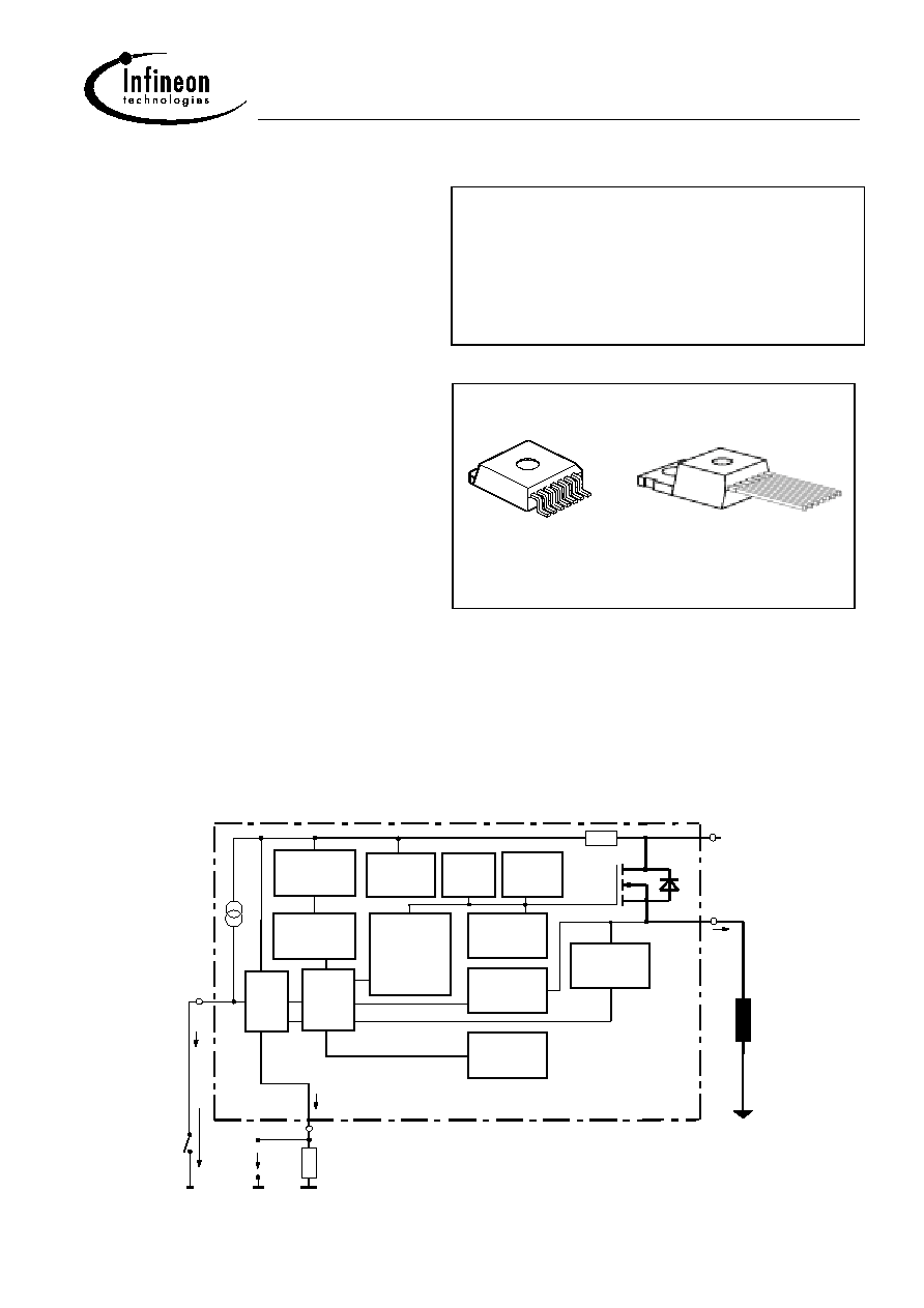
Smart Highside Power Switch
Reversave
∑
Reverse battery protection by self turn on of
power MOSFET
Features
∑
Short circuit protection with latch
∑
Current limitation
∑
Overload protection
∑
Thermal shutdown with restart
∑
Overvoltage protection (including load dump)
∑
Loss of ground protection
∑
Loss of V
bb
protection (with external diode for
charged inductive loads)
∑
Very low standby current
∑
Fast demagnetization of inductive loads
∑
Electrostatic discharge (ESD) protection
∑
Optimized static electromagnetic compatibility
(EMC)
Diagnostic Function
∑
Proportional load current sense (with defined fault
signal in case of overload operation, overtemperature shutdown and/or short circuit shutdown)
Application
∑
Power switch with current sense diagnostic feedback for 12V and 24 V DC grounded loads
∑
All types of resistive, inductive and capacitive loads
∑
Replaces electromechanical relays, fuses and discrete circuits
General Description
N channel vertical power FET with charge pump, current controlled input and diagnostic feedback with load
current sense, integrated in Smart SIPMOS
chip on chip technology. Providing embedded protective functions.
IN
Charge pump
Level shifter
Rectifier
Limit for
unclamped
ind. loads
Gate
protection
Current
limit
3
Overvoltage
protection
+ V bb
PROFET
OUT
4 & Tab
1, 2, 6, 7
Load GND
Load
Output
Voltage
detection
R
IS
IS
5
I
IS
I
L
V
IS
I
IN
Logic GND
Voltage
sensor
Voltage
source
Current
Sense
Logic
ESD
Temperature
sensor
R bb
V
IN
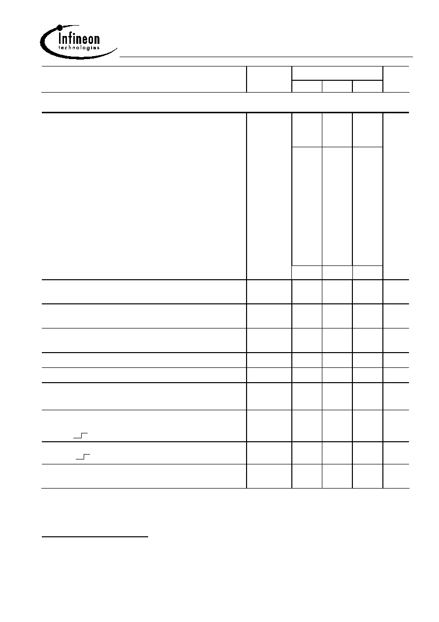
Product Summary
Operating voltage
V
bb(on)
5.5
...
38
V
On-state resistance
R
ON
9
m
Nominal current
I
L(nom)
9.5
A
Load current (ISO)
I
L(ISO)
37.5
A
Current limitation
I
L12(SC)
90
A
Package
TO 220-7-180
TO 220-7-230
S M D
1
7

Data sheet BTS 6144B/P
Infineon Technologies AG Page 2 of 16 2003-Oct-01
Pin Symbol
Function
1; 2
OUT
O
Output; output to the load; pin 1, 2, 6 and 7 must be externally shorted* .
3 IN I
Input; activates the power switch if shorted to ground.
4; Tab
Vbb +
Supply
Voltage; positive power supply voltage; tab and pin4 are internally
shorted.
5 IS S
Sense
Output; Diagnostic feedback; provides at normal operation a sense
current proportional to the load current; in case of overload,
overtemperature and/or short circuit a defined current is provided (see
Truth Table on page 8)
6; 7
OUT
O
Output; output to the load; pin 1, 2, 6 and 7 must be externally shorted* .
*) Not shorting all outputs will considerably increase the on-state resistance, reduce the peak current capability
and decrease the current sense accuracy
Maximum Ratings at T
j
= 25 ∞C unless otherwise specified
Parameter Symbol
Values
Unit
Supply voltage (overvoltage protection see page 4)
V
bb
38
V
Supply voltage for full short circuit protection
1)
V
bb
30
V
Load dump protection V
LoadDump
= U
A
+ V
s
, U
A
= 13.5 V
R
I
= 2
, R
L
= 1
, t
d
= 400 ms, IN= low or high
V
Load dump
2
)
45
V
Load current (Short-circuit current, see page 5)
I
L
self-limited
A
Operating temperature range
Storage temperature range
T
j
T
stg
-40 ...+150
-55 ...+150
∞C
Power dissipation (DC)
P
tot
81
W
Inductive load switch-off energy dissipation m
3)
single pulse, I
L
= 20 A, V
bb
= 12V
T
j
=150 ∞C:
E
AS
0.4
J
Electrostatic discharge capability (ESD)
(Human Body Model)
acc.
ESD assn. std. S5.1-1993; R=1.5k
; C=100pF
V
ESD
3.0
kV
Current through input pin (DC)
Current through current sense pin (DC)
see internal circuit diagrams page 9
I
IN
I
IS
+15, -120
+15, -120
mA
Input voltage slew rate
V
bb
16V :
V
bb
> 16V
4)
:
dV
bIN
/ dt
self-limited
20
V/
µ
s
1)
Short circuit is defined as a combination of remaining resistances and inductances. See schematic on
page11.
2)
V
Load dump
is setup without the DUT connected to the generator per ISO 7637-1 and DIN 40839
3)
See also diagram on page 11.
4)
See also on page 8. Slew rate limitation can be achieved by means of using a series resistor R
IN
in the input
path. This resistor is also required for reverse operation. See also page 10.

Data sheet BTS 6144B/P
Infineon Technologies AG Page 3 of 16 2003-Oct-01
Thermal Characteristics
Parameter and Conditions Symbol
Values
Unit
min typ
max
Thermal resistance
chip - case
:
R
thJC
5
)
-- 0.7 0.8
K/W
junction - ambient (free air):
R
thJA
--
60 --
SMD version, device on PCB
6
):
--
33
40
5)
Thermal resistance R
thCH
case to heatsink (about 0.5 ... 0.9 K/W with silicone paste) not included!
6
) Device on 50mm*50mm*1.5mm epoxy PCB FR4 with 6cm
2
(one layer, 70
µ
m thick) copper area for Vbb
connection. PCB is vertical without blown air.
Electrical Characteristics
Parameter and Conditions Symbol
Values
Unit
at T
j
= 25, V
bb
= 12 V unless otherwise specified
min typ
max
Load Switching Capabilities and Characteristics
On-state resistance (pin 3 to pin 1,2,6,7)
V
IN
= 0, V
bb
= 5.5V, I
L
= 10 A
T
j
=25 ∞C:
T
j
=150 ∞C:
V
IN
= 0, V
bb
= 12V, I
L
= 10 A
T
j
=25 ∞C:
T
j
=150 ∞C:
R
ON
--
--
--
--
9.5
17
7
13
13
22
9
16
m
Output voltage drop limitation at small load
currents (Tab to pin 1,2,6,7)
T
j
=-40...150 ∞C:
V
ON(NL)
-- 30 60
mV
Nominal load current (Tab to pin 1,5)
ISO Proposal: V
ON
0.5 V, T
C
= 85∞C, T
j
150∞C
SMD
6)
, V
ON
0.5 V, T
A
= 85∞C, T
j
150∞C
I
L(ISO)
I
L(nom)
37.5
9.5
48
12
--
--
A
Turn-on time
to 90% V
OUT
:
Turn-off time
to 10% V
OUT
:
R
L
= 2.2
,
T
j
=-40...150 ∞C
t
on
t
off
--
--
300
300
550
600
µ
s
Slew rate on
25 to 50% V
OUT
,
R
L
= 2.2
,
T
j
=-40...150 ∞C
dV /dt
on
--
0.2
0.35
V/
µ
s
Slew rate off
50 to 25% V
OUT
, R
L
= 2.2
,
T
j
=-40...150 ∞C
-dV/dt
off
--
0.2
0.45
V/
µ
s

Data sheet BTS 6144B/P
Parameter and Conditions Symbol
Values
Unit
at T
j
= 25, V
bb
= 12 V unless otherwise specified
min typ
max
Infineon Technologies AG Page 4 of 16 2003-Oct-01
Operating Parameters
Operating voltage (V
IN
=0)
T
j
=-40...150 ∞C: V
bb(on)
5.5
--
38
V
Undervoltage shutdown
7
)
8
)
V
bIN(u)
-- 2.5 3.5
V
Undervoltage restart of charge pump
V
bb(ucp)
--
4
5.5
V
Overvoltage protection
9
)
I
bb
=15 mA
T
j
=-40...+150∞C
:
V
Z,IN
63
67
--
V
Standby current
T
j
=-40...+120∞C
:
I
IN
=0
T
j
=150∞C:
I
bb(off)
--
--
3
6
6
14
µ
A
Reverse Battery
Reverse battery voltage
10)
-V
bb
--
--
16
V
On-state resistance (pin 4, Tab to pin 1,2,6,7)
V
bb
= - 8V, V
IN
= 0, I
L
= -10 A, R
IS
= 1 k
,
8)
T
j
=25 ∞C:
T
j
=150 ∞C:
V
bb
= -12V, V
IN
= 0, I
L
= -10 A, R
IS
= 1 k
, T
j
=25 ∞C:
T
j
=150 ∞C:
R
ON(rev)
--
--
--
--
8.5
13
8
13
12
18
11
19
m
Integrated resistor in V
bb
line
R
bb
-- 100 150
Inverse Operation
11)
Output voltage drop (pin 4, Tab to pin 1,2,6,7)
8)
I
L
= -10 A, R
IS
= 1 k
,
T
j
=25 ∞C:
I
L
= -10 A, R
IS
= 1 k
,
T
j
=150 ∞C:
-V
ON(inv)
--
--
700
300
--
--
mV
Turn-on delay after inverse operation; I
L
> 0A
8)
V
IN
(inv) = V
IN
(fwd) = 0 V
t
d(inv)
--
1 --
ms
7)
V
bIN
=V
bb
-V
IN
see diagram page 14.
8)
not subject to production test, specified by design
9)
See also V
ON(CL)
in circuit diagram page 9.
10)
For operation at voltages higher then |16V| please see required schematic on page 10.
11)
Permanent Inverse operation results eventually in a current flow via the intrinsic diode of the power DMOS.
In this case the device switches on with a time delay t
d(inv)
)
after the transition from inverse to forward mode.

Data sheet BTS 6144B/P
Parameter and Conditions Symbol
Values
Unit
at T
j
= 25, V
bb
= 12 V unless otherwise specified
min typ
max
Infineon Technologies AG Page 5 of 16 2003-Oct-01
Protection Functions
12
)
Short circuit current limit (pin 4, Tab to
pin 1,2,6,7)
13
)
Short circuit current limit at
V
ON
= 6V
14)
T
j
=-40∞C:
T
j
=25∞C:
T
j
=+150∞C:
I
L6(SC)
--
--
90
140
130
120
170
--
--
A
Short circuit current limit at
V
ON
= 12V
T
j
=-40∞C:
t
m
=170µs
T
j
=25∞C:
T
j
=+150∞C:
I
L12(SC)
--
--
55
105
95
85
130
--
--
A
Short circuit current limit at
V
ON
= 18V
14
)
T
j
=-40∞C:
T
j
=25∞C:
T
j
=+150∞C:
I
L18(SC)
--
--
45
75
70
65
100
--
--
A
Short circuit current limit at
V
ON
= 24V
T
j
=-40∞C:
t
m
=170µs
T
j
=25∞C:
T
j
=+150∞C:
I
L24(SC)
--
--
28
47
46
45
70
--
--
A
Short circuit current limit at
V
ON
= 36V
14)
T
j
=-40∞C:
T
j
=25∞C:
T
j
=+150∞C:
I
L36(SC)
--
--
15
27
27
27
40
--
--
A
Short circuit shutdown detection voltage
V
ON(SC)
2.5 3.5 4.5
V
Short circuit shutdown delay after input current
positive slope, V
ON
> V
ON(SC),
T
j
=
-40...+150∞C
min. value valid only if input "off-signal" time exceeds 30
µ
s
t
d(SC1)
350
650 1200
µ
s
Short circuit shutdown delay during on condition
14)
V
ON
> V
ON(SC)
t
d(SC2)
--
2 --
µ
s
Output clamp (inductive load switch off)
15
)
at V
OUT
= V
bb
- V
ON(CL)
(e.g. overvoltage)
I
L
= 40 mA
V
ON(CL)
39
42 --
V
Thermal overload trip temperature
T
jt
150
175
--
∞C
Thermal hysteresis
T
jt
-- 10 --
K
12)
Integrated protection functions are designed to prevent IC destruction under fault conditions described in the
data sheet. Fault conditions are considered as "outside" normal operating range. Protection functions are
not designed for continuous repetitive operation.
13
) Short circuit current limit for max. duration of t
d(SC1)
, prior to shutdown, see also figures 3.x on page 13.
14
) not subject to production test, specified by design
15
) See also figure 2b on page 12.
Data sheet BTS 6144B/P
Parameter and Conditions Symbol
Values
Unit
at T
j
= 25, V
bb
= 12 V unless otherwise specified
min typ
max
Infineon Technologies AG Page 6 of 16 2003-Oct-01
Diagnostic Characteristics
Current sense ratio, static on-condition
k
ILIS
=
I
L
:
I
IS
, I
IS
< I
IS,lim
16)
,
V
IS
<V
OUT
-
5
V, V
bIN
>
4.5
V
k
ILIS
--
12500
--
IL = 35A, Tj = -40∞C:
Tj = +25∞C:
Tj = +150∞C:
IL = 10A, Tj = -40∞C:
Tj = +25∞C:
Tj = +150∞C:
IL = 2.5A, Tj = -40∞C:
Tj = +25∞C:
Tj = +150∞C:
IL = 0.5A, Tj = -40∞C:
Tj = +25∞C:
Tj = +150∞C:
11200
11000
11000
10500
10500
10800
10000
10000
10000
7000
8000
9000
12700
12600
12200
12700
12600
12200
12300
12500
13000
14000
14500
15000
14000
13500
12800
14300
14000
13300
17000
16500
15000
26000
24500
23000
I
IN
= 0
(e.g. during deenergizing of inductive loads)
:
-- 0
--
Sense current under fault conditions
17)
VON>1V, typ
T
j
=
-40...+150∞C:
I
IS,fault
4.0
5.2 7.5
mA
Sense saturation current
VON<1V, typ
T
j
=
-40...+150∞C:
I
IS,lim
4.0
6.0 7.5
mA
Fault-Sense signal delay after input current positive
slope, V
ON
>1V,
Tj = -40...+150∞C
t
delay(fault)
350 650
1200
µ
s
Current sense leakage current, I
IN
=
0
I
IS(LL)
-- 0.1
0.5
µ
A
Current sense offset current, V
IN
=
0, I
L
0
I
IS(LH)
-- 0.1
1
µ
A
Minimum load current for sense functionality,
V
IN
=
0, Tj = -40...+150∞C
I
L(MIN)
50 --
--
mA
Current sense settling time to I
IS static
after input
current positive slope,
18
)
I
L
= 0
20 A, T
j
= -40...+150∞C
t
son(IS)
--
250
500
µ
s
Current sense settling time during on condition,
18)
I
L
= 10
20 A, T
j
= -40...+150∞C
t
slc(IS)
--
50
100
µ
s
Overvoltage protection
I
bb
=
15
mA
T
j
=
-40...+150∞C:
V
Z,IS
63
67
--
V
16)
See also figures 4.x and 6.x on page 13 and 14.
17)
Fault conditions are overload during on (i.e. V
ON
>1V typ.), overtemperature and short circuit; see also truth
table on page 8.
18
) not subject to production test, specified by design

Data sheet BTS 6144B/P
Parameter and Conditions Symbol
Values
Unit
at T
j
= 25, V
bb
= 12 V unless otherwise specified
min typ
max
Infineon Technologies AG Page 7 of 16 2003-Oct-01
Input
Required current capability of input switch
T
j
=-40..+150∞C:
I
IN(on)
-- 1.4 2.2
mA
Input current for turn-off
T
j
=-40..+150∞C: I
IN(off)
-- --
30
µA
Data sheet BTS 6144B/P
Infineon Technologies AG Page 8 of 16 2003-Oct-01
Truth Table
Input
Current
level
Output
level
Current
Sense
I
IS
Normal
operation
L
H
L
H
0 (I
IS(LL)
)
nominal
Overload
19
)
L
H
L
H
0 (I
IS(LL)
)
I
IS,fault
Short circuit to GND
20
)
L
H
L
L
0 (I
IS(LL)
)
I
IS,fault
Overtemperature L
H
L
L
0 (I
IS(LL)
)
I
IS,fault
Short circuit to Vbb
L
H
H
H
0 (I
IS(LL)
)
<nominal
21)
Open load
L
H
Z
H
0 (I
IS(LL)
)
0 (I
IS(LH)
)
L = "Low" Level
Z = high impedance, potential depends on external circuit
H = "High" Level
19
) Overload is detected at the following condition: 1V (typ.) < V
ON
< 3.5V (typ.) . See also page 11.
20
) Short Circuit is detected at the following condition: V
ON
> 3.5V (typ.) . See also page 11.
21
) Low ohmic short to
V
bb
may reduce the output current
I
L
and therefore also the sense current
I
IS
.
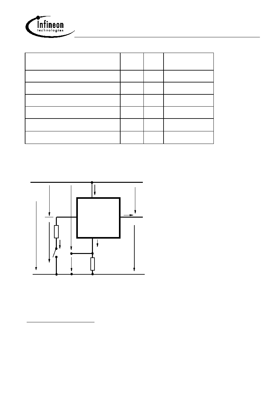
Terms
PROFET
V
IN
IS
OUT
bb
V
IN
I
IS
I
IN
V
bb
Ibb
IL
V
OUT
V
ON
3
5
4
1,2,6,7
R
IS
V
IS
V
bIN
R
IN
D
S
V
bIS
Two or more devices can easily be connected in
parallel to increase load current capability.
Data sheet BTS 6144B/P
Infineon Technologies AG 9 of 16 2003-Oct-01
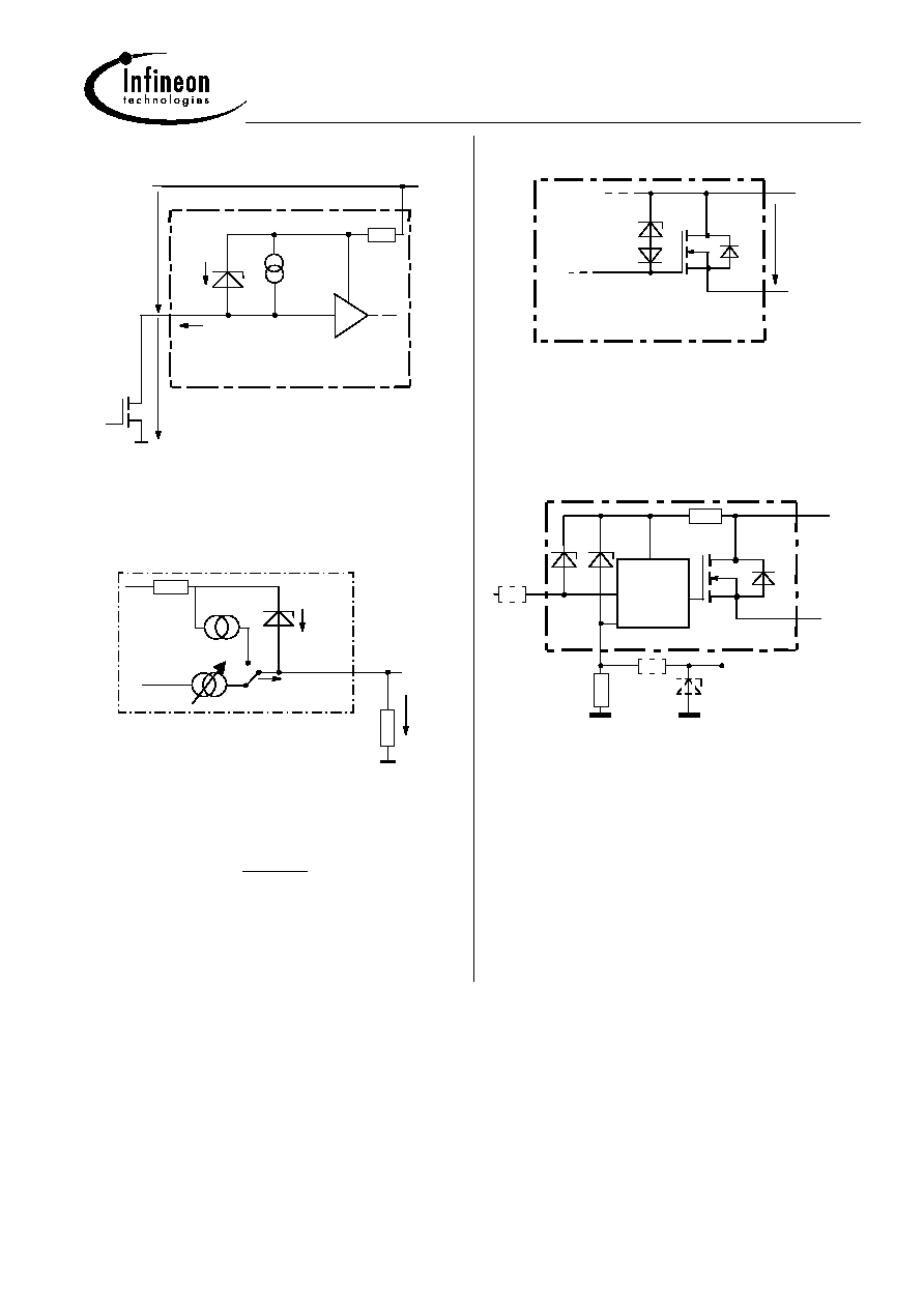
Input circuit (ESD protection)
IN
ZD
IN
I
V bb
Rbb
V
Z,IN
V bIN
V IN
ESD-Zener diode: 67 V typ., max 15 mA;
Current sense output
Normal operation
IS
IS
R
ZD
IS
V
Vbb
Z,IS
V
Rbb
IIS
IIS,fault
V
Z,IS
=
67
V
(typ.), R
IS
=
1
k
nominal (or 1
k
/n, if n
devices are connected in parallel). I
S
= I
L
/k
ilis
can be
only driven by the internal circuit as long as
V
out
- V
IS
>
5V. Therefore R
IS
should be less than
mA
V
V
bb
5
.
7
5
-
.
Note: For large values of R
IS
the voltage V
IS
can reach
almost V
bb
. See also overvoltage protection.
If you don't use the current sense output in your
application, you can leave it open.
Inductive and overvoltage output clamp
+ V
bb
OUT
PROFET
V
Z1
V
ON
V
ON
is clamped to V
ON(Cl)
=
42V typ
Overvoltage protection of logic part
+ V
bb
V
OUT
IN
bb
R
Signal GND
Logic
PROFET
V
Z,IS
R
IS
IN
R
IS
V
Z,IN
R
V
V
Z,VIS
R
bb
=
100
typ
.
,
V
Z,IN
= V
Z,IS
=
67
V
typ.,
R
IS
=
1
k
nominal. Note that when overvoltage exceeds 67
V
typ.
a voltage above 5V can occur between IS and GND, if
R
V
, V
Z,VIS
are not used.

Data sheet BTS 6144B/P
Infineon Technologies AG 10 of 16 2003-Oct-01
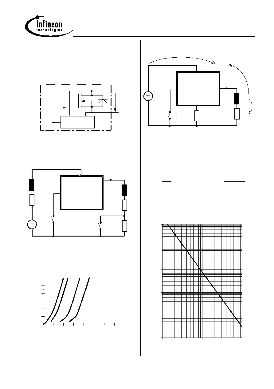
Reversave
(
Reverse battery protection)
Logic
IN
IS
R
OUT
L
R
Power GND
Signal GND
Vbb
-
Power
Transistor
IN
R
bb
R
D
R
IS
typ. 1
k
. Add
R
IN
for reverse battery protection in
applications with
V
bb
above 16V;
recommended value:
=
+
IS
IN
R
R
1
1
V
V
A
bb
12
|
|
08
.
0
-
To minimise power dissipation at reverse battery
operation, the overall current into the IN and IS pin
should be about 80mA. The current can be provided by
using a small signal diode D in parallel to the input
switch, by using a MOSFET input switch or by proper
adjusting the current through R
IS.
Since the current via R
bb
generates additional heat in
the device, this has to be taken into account in the
overall thermal consideration.
Inverse load current operation
PROFET
V
IN
OUT
IS
bb
V
bb
V
OUT
- I
L
R
IS
V
IS
V
IN
+
-
+
-
I
IS
The device can be operated in inverse load current
mode (V
OUT
> V
bb
> 0V). The current sense feature is
not available during this kind of operation (I
IS
= 0). In
case of inverse operation the intrinsic drain source
diode is eventually conducting resulting in considerably
increased power dissipation.
The transition from inverse to forward mode can result
in a delayed switch on.
Note: Temperature protection during inverse load
current operation is not possible!
V
bb
disconnect with energised inductive
load
Provide a current path with load current capability by
using a diode, a Z-diode, or a varistor. (V
ZL
+V
D
<39 V if
R
IN
=
0). For higher clamp voltages currents at IN and
IS have to be limited to
120 mA.
Version a:
PROFET
V
IN
OUT
IS
bb
V
bb
V
ZL
V
D
Data sheet BTS 6144B/P
Infineon Technologies AG 11 of 16 2003-Oct-01
Short circuit detection
Fault Condition: V
ON
> V
ON(SC)
(3.5
V typ.) and t> t
d(SC)
(typ.650 µs).
Overload detection
Fault Condition: V
ON
> 1
V typ.
detection
circuit
Logic
unit
+ Vbb
O UT
V
O N
Short circuit
Short circuit is a combination of primary and
secondary impedance's and a resistance's.
PROFET
V
IN
OUT
IS
bb
RSC
I
IN
V bb
Z
L
SC
L SC
10mOhm
5uH
A
llowable combinations of minimum, secondary
resistance for full protection at given secondary
inductance and supply voltage for single short circuit
event:
0
5
16V
10
0
100
200
RSC
[mOhm]
15
L SC
300
[uH]
V :
bb
18V
24V
30V
Inductive load switch-off energy
dissipation
PROFET
V
IN
OUT
IS
bb
E
E
E
EAS
bb
L
R
ELoad
L
RL
{
Z L
RIS
I
IN
Vbb
i (t)
L
Energy stored in load inductance:
E
L
=
1/2
∑
L
∑
I
2
L
While demagnetizing load inductance, the energy
dissipated in PROFET is
E
AS
= E
bb
+ E
L
- E
R
=
V
ON(CL)
∑
i
L
(t) dt,
with an approximate solution for RL
>
0
:
E
AS
=
I
L
∑
L
2
∑
R
L
(
V
bb
+
|V
OUT(CL)
|)
ln
(1+
I
L
∑
R
L
|V
OUT(CL)
|
)
Maximum allowable load inductance for
a single switch off
L = f (IL );
Tj,start =
150∞C, Vbb =
12
V, RL =
0
0,0 1
0,1
1
1 0
10 0
100 0
1
10
10 0
I_ L [A ]
L [m H ]
Data sheet BTS 6144B/P
Infineon Technologies AG 12 of 16 2003-Oct-01
Timing diagrams
Figure 1a: Switching a resistive load,
change of load current in on-condition:
I
IN
t
V
OUT
I
L
I
IS
t
son(IS)
t
t
slc(IS)
Load 1
Load 2
soff(IS)
t
t
t
on
off
slc(IS)
90%
dV/dton
dV/dtoff
10%
The sense signal is not valid during a settling time
after turn-on/off and after change of load current.
Figure 2a: Switching motors and lamps:
I
IN
t
V
OUT
I
IL
I
IS
I
IS,faut
/ I
IS,lim
As long as VbIS < VZ,IS the sense current will never
exceed IIS,fault and/or IIS,lim.
Figure 2b: Switching an inductive load:
I
IN
t
V
OUT
I
L
I
IS
V
ON(CL)
Data sheet BTS 6144B/P
Infineon Technologies AG 13 of 16 2003-Oct-01
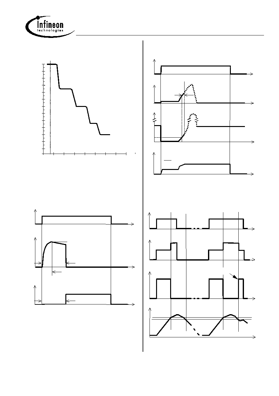
Figure 3a: Typ. current limitation characteristic
0
10
20
VON
[V]
[A]
IL(SC)
30
V
ON(SC)
0
20
40
60
80
100
120
In case of V
ON
> V
ON(SC)
(typ. 3.5 V) the device will
be switched off by internal short circuit detection.
Figure 3b: Short circuit type one:
shut down by short circuit detection, reset by I
IN
=
0.
I
IN
I
L
I
L(SC)
I
IS
t
t
d(SC1)
I
IS,fault
t
delay(fault)
t
m
V
ON
> V
ON(SC)
Shut down remains latched until next reset via input.
Figure 3c: Short circuit type two:
shut down by short circuit detection, reset by I
IN
=
0.
I
IN
I
L
Internal Switch off
I
IS
t
t
d(SC2)
I
IS,fault
V
ON
I
L
k
ilis
1V typ.
depending on the
external impedance
Shut down remains latched until next reset via input.
Figure 4a: Overtemperature
Reset if T
j
<T
jt
I
IN
t
I
IS
V
OUT
T
j
IIS,fault
Auto Restart
Data sheet BTS 6144B/P
Infineon Technologies AG 14 of 16 2003-Oct-01
Figure 4b: Overload
T
j
<T
jt
I
IN
t
I
L
V
bb
I
S
-V
OUT
V =1V typ.
ON
R *I
ON L,lim
I
L
k
ilis
I
IS,lim
I
IS,fault
Figure 5a: Undervoltage restart of charge pump,
overvoltage clamp
0
0
10
12
V
OUT
V
bIN(ucp)
V
IN
= 0
I
IN
= 0
V
ON(CL)
V
ON(CL)
V
bIN(u)
V
bIN(u)
dynamic, short
Undervoltage
not below
V
bb
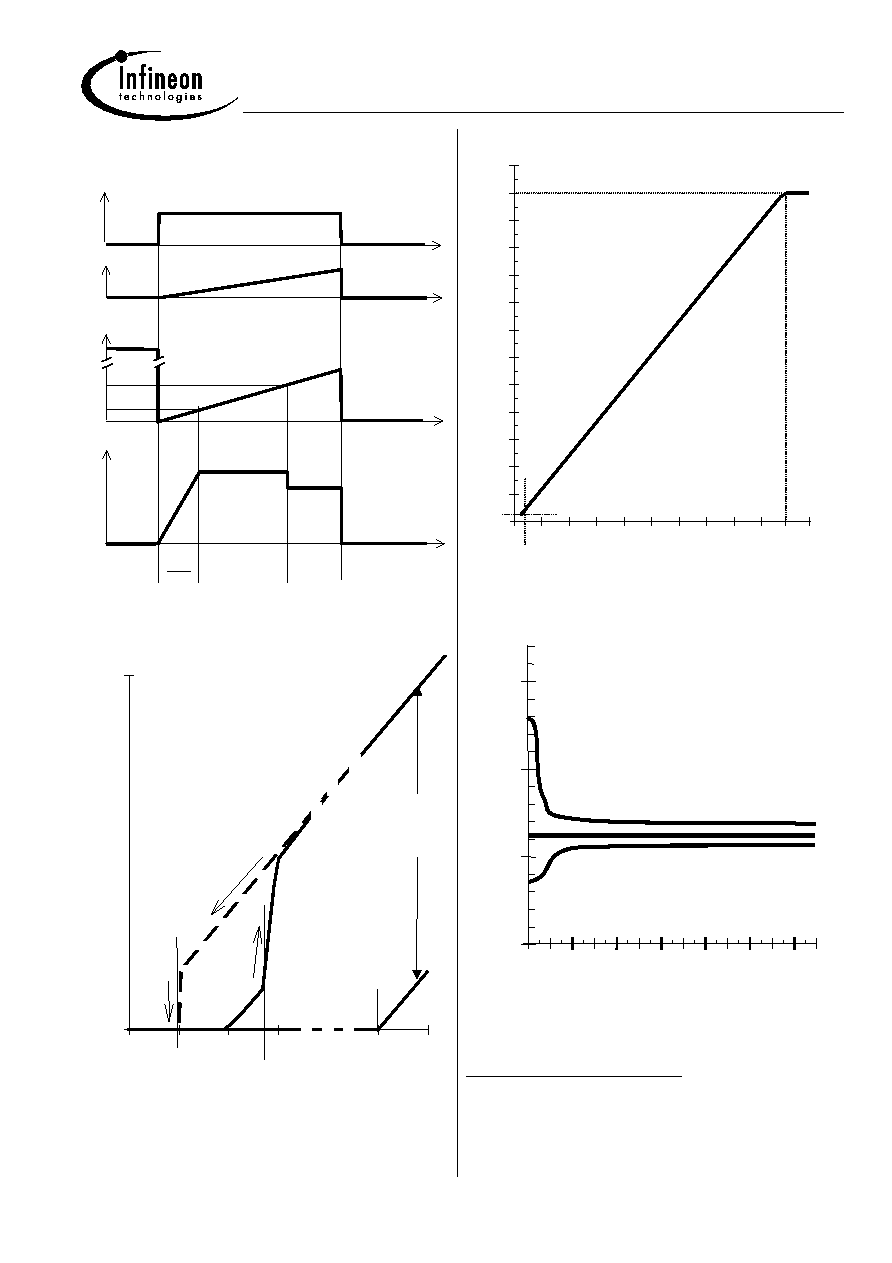
Figure 6a: Current sense versus load current:
0
1
2
I L
[A]
[mA] IIS
10
20
30
40
3
I
IS,lim
4
I
IS(LH)
50
I
L,lim
I
L(MIN)
Figure 6b: Current sense ratio
22
:
0
20000
0
10
20
IL
[A]
kILIS
5
30000
10000
30
22
This range for the current sense ratio refers to all
devices. The accuracy of the k
ILIS
can be raised by
means of calibration the value of k
ILIS
for every
single device.
Data sheet BTS 6144B/P
Infineon Technologies AG 15 of 16 2003-Oct-01
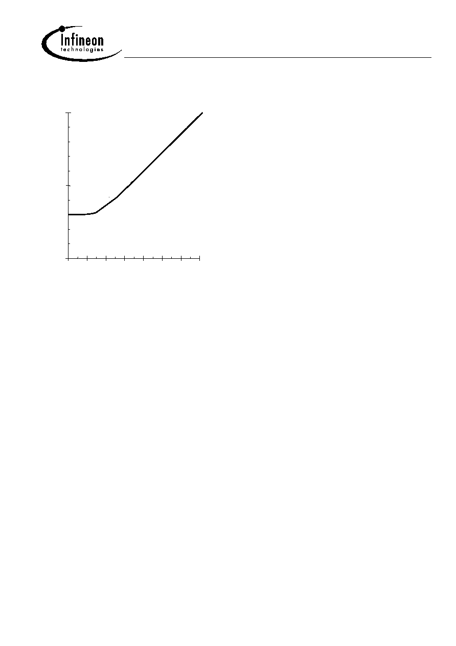
Figure 7a: Output voltage drop versus load current:
0.0
0.05
0.1
0
2
4
6
8
10
14
I L
[A]
[V]
VON
ON(NL)
V
ON
R
Data sheet BTS 6144B/P
Infineon Technologies AG 16 of 16 2003-Oct-01
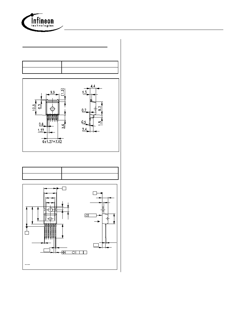
Package and Ordering Code
All dimensions in mm
SMD:TO-220-7-180
Sales code
BTS6144B
Ordering code
Q67060-S6058-A102
Standard (straight): TO220-7-230
Sales code
BTS6144P
Ordering code
Q67060-S6320-A102
All metal surfaces tin plated, except area of cut.
Shear and punch direction no burrs this surface.
±0.5
Back side, heatsink contour
1.27
1)
C
6x
0...0.15
0.6
7x
±0.1
0.25
M
12.5
±0.3
15.6
17.5
±0.3
13
7.5
2.8
±0.2
6.6
3.7
-0.15
±0.2
±0.2
9.9
9.5
A
B
A
C
4.4
1)
0.05
+0.1
-0.02
1.3
B
±0.2
9.2
±0.1
0.5
2.4
Published by
Infineon Technologies AG,
St.-Martin-Strasse 53,
D-81669 M¸nchen
© Infineon Technologies AG 2001
All Rights Reserved.
Attention please!
The information herein is given to describe certain
components and shall not be considered as a guarantee
of characteristics.
Terms of delivery and rights to technical change
reserved.
We hereby disclaim any and all warranties, including but
not limited to warranties of non-infringement, regarding
circuits, descriptions and charts stated herein.
Infineon Technologies is an approved CECC
manufacturer.
Information
For further information on technology, delivery terms and
conditions and prices please contact your nearest
Infineon Technologies Office in Germany or our Infineon
Technologies Representatives worldwide (see address
list).
Warnings
Due to technical requirements components may contain
dangerous substances. For information on the types in
question please contact your nearest Infineon
Technologies Office.
Infineon Technologies Components may only be used in
life-support devices or systems with the express written
approval of Infineon Technologies, if a failure of such
components can reasonably be expected to cause the
failure of that life-support device or system, or to affect
the safety or effectiveness of that device or system. Life
support devices or systems are intended to be implanted
in the human body, or to support and/or maintain and
sustain and/or protect human life. If they fail, it is
reasonable to assume that the health of the user or other
persons may be endangered.