
INFINEON Technologies
1
9.01
HYS 64V16302GU
SDRAM-Modules
3.3 V 16M
◊
64-Bit, 128MByte SDRAM Module
168-pin Unbuffered DIMM Modules
Description
The HYS 64V16302 is an industry standard 168-pin 8-byte Dual in-line Memory Module (DIMM)
which is organized as 16M
◊
64 in an one bank high speed memory arrays designed with 256 Mbit
Synchronous DRAMs for non-parity applications. The DIMMs use -7 speed sorted 16M
◊
16
organised 256Mbit SDRAM devices in TSOP54 packages to meet the PC133-222 requirements, -
7.5 for PC133-333 and -8 parts for the standard PC100 applications. Decoupling capacitors are
mounted on the PC board. The PC board design is according to INTEL's module specification.
The DIMMs have a serial presence detect, implemented with a serial E2PROM using the 2-pin I
2
C
protocol. The first 128 bytes are utilized by the DIMM manufacturer and the second 128 bytes are
available to the end user.
All Infineon 168-pin DIMMs provide a high performance, flexible 8-byte interface in a 133.35 mm
long footprint.
Important Notice:
This module, which is based on 256MBit device technology can only be used in applications, where
the 256Mbit addressing is supported.
∑ 168 Pin unbuffered 8 Byte Dual-In-Line
SDRAM Modules for PC main memory
applications using 256Mbit technology
∑ PC100-222, PC133-333 and PC133-222
versions
∑ One bank 16M
◊
64 organization
∑ Optimized for byte-write non-parity
∑ JEDEC standard Synchronous DRAMs
(SDRAM)
∑ Single 3.3 V (
±
0.3 V) power supply
∑ SDRAM Performance:
∑ Programmed Latencies:
∑ Programmable CAS Latency, Burst Length,
and Wrap Sequence
(Sequential & Interleave)
∑ Auto Refresh (CBR) and Self Refresh
∑ Decoupling capacitors mounted on substrate
∑ All inputs and outputs are LVTTL compatible
∑ Serial Presence Detect with E
2
PROM
∑ Utilizes 16M
◊
16 (256Mbit SDRAMs in
TSOPII-54 packages with
8096 refresh cycles every 64 ms
∑ 133.35 mm
◊
29.21 mm
◊
3.00 mm card size
with gold contact pads
(JEDEC MO-161)
-7/ -7.5 -8
Unit
PC133
PC100
f
CK
Clock
Frequency
(max.)
133
100
MHz
t
AC
Clock Access
Time
5.4
6
ns
Product Speed
CL
t
RCD
t
RP
-7
PC133
2
2
2
-7.5
PC133
3
3
3
-8
PC100
2
2
2

HYS 64V16302GU
SDRAM-Modules
INFINEON Technologies
2
9.01
Note: All part numbers end with a place code (not shown), designating the die revision. Consult
factory for current revision. Example: HYS64V16302GU-8-C2, indicating Rev.C2 dies are
used for SDRAM components.
Ordering Information
Type
Code
Package
Description
Module
Height
HYS 64V16302GU-7-D
PC133-222-520 L-DIM-168-32 133 MHz CL=2 16M
◊
64
one bank SDRAM module
HYS 64V16302GU-7.5-C2
HYS 64V16302GU-7.5-D
PC133-333-520 L-DIM-168-32 133 MHz CL=3 16M
◊
64
one bank SDRAM module
1.15"
HYS 64V16302GU-8-C2
PC100-222-620 L-DIM-168-32 100 MHz CL=2 16M
◊
64
one bank SDRAM module
1.15"
Pin Definitions and Functions
A0 - A12
Address Inputs
CLK0 - CLK3
Clock Input
BA0, BA1
Bank Select
DQMB0 - DQMB7
Data Mask
DQ0 - DQ63
Data Input/Output
CS0, CS2
Chip Select
CB0 - CB7
Check Bits (x72
organization only)
V
DD
Power (+ 3.3 V)
RAS
Row Address Strobe
V
SS
Ground
CAS
Column Address Strobe
SCL
Clock for Presence Detect
WE
Read/Write Input
SDA
Serial Data Out for Pres. Detect
CKE0
Clock Enable
N.C./DU
No Connection
Address Format
Part Number
Rows Columns Bank Select
Refresh
Period
Interval
16M
◊
64
HYS64V16302GU 13
9
2
8k
64 ms
7,8
µ
s
HYS 64V16302GU
SDRAM-Modules
INFINEON Technologies
4
9.01
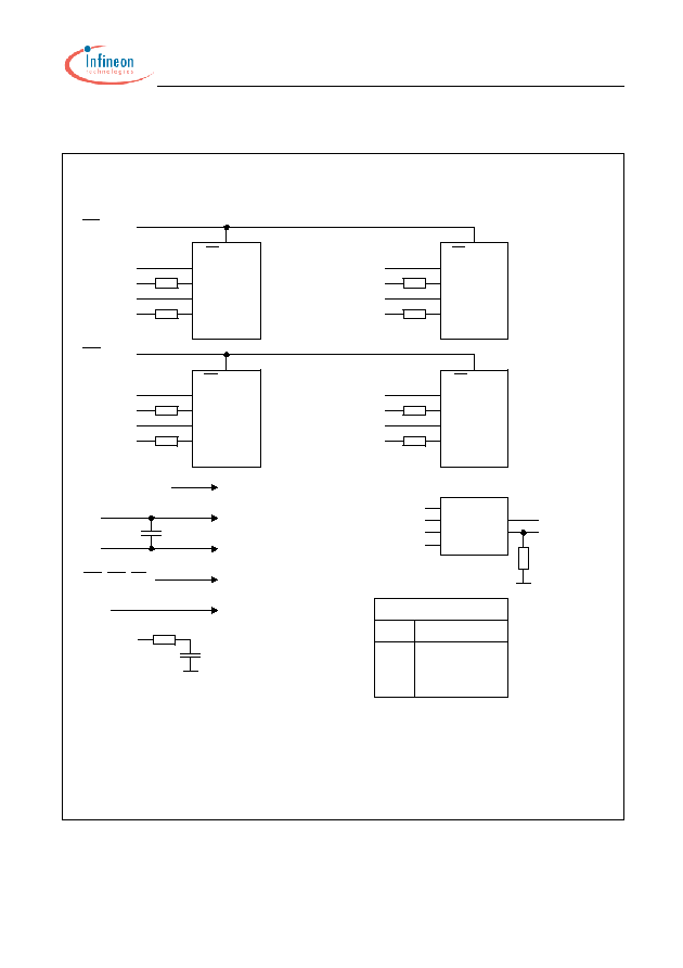
Functional Block Diagrams
Block Diagram: 16M x 64 One Bank SDRAM DIMM Modules (HYS 64V16302GU)
BL03 7.8.00
DQ0-DQ7
LDQM
CS, CLK
D0
CS0, CLK0
DQ32-DQ39
DQMB4
DQ0-DQ7
DQ40-DQ47
DQMB5
LDQM
D1
CS, CLK
A0-A12, BA0, BA1
D0-D3
CC
V
SS
V
C
RAS, CAS, WE
CKE0
CLK1, CLK3
Clock Wiring
8 M x 64
CLK0
2 SDRAM + 3.3 pF
Termination
CLK1
2 SDRAM + 3.3 pF
CLK2
CLK3
47 k
SCL
SCL
2
SA0
SA1
SA2
E PROM (256 word x 8 Bit)
SA1
SA0
SA2
SDA
WP
DQMB0
DQ0-DQ7
DQMB1
DQ8-DQ15
UDQM
DQ8-DQ15
UDQM
DQ8-DQ15
DQ24-DQ31
DQ56-DQ63
DQMB7
DQMB3
DQMB2
DQ16-DQ23
DQMB6
DQ48-DQ55
CS2, CLK2
CS, CLK
DQ8-DQ15
UDQM
LDQM
DQ0-DQ7
D2
CS, CLK
DQ8-DQ15
UDQM
LDQM
DQ0-DQ7
D3
All resistors are 10 Ohm except otherwise noted
Notes:
1)
10 pF
D0-D3
D0-D3
D0-D3
D0-D3
Termination

HYS 64V16302GU
SDRAM-Modules
INFINEON Technologies
5
9.01
Absolute Maximum Ratings
Parameter
Symbol
Limit Values
Unit
min.
max.
Input / Output voltage relative to V
SS
V
IN,
V
OUT
≠ 1.0
4.6
V
Power supply voltage on V
DD
V
DD,
≠ 1.0
4.6
V
Storage temperature range
T
STG
-55
+150
o
C
Power dissipation
P
D
≠
4
W
Data out current (short circuit)
I
OS
≠
50
mA
Permanent device damage may occur if "Absolute Maximum Ratings" are exceeded.
Functional operation should be restricted to recommended operation conditions.
Exposure to higher than recommended voltage for extended periods of time affect device reliability
DC Characteristics
T
A
= 0 to 70
∞
C;
V
SS
= 0 V;
V
DD
= 3.3 V
±
0.3 V
Parameter
Symbol
Limit Values
Unit
min.
max.
Input High Voltage
V
IH
2.0
V
DD
+ 0.3
V
Input Low Voltage
V
IL
≠ 0.5
0.8
V
Output High Voltage (
I
OUT
= ≠ 4.0 mA)
V
OH
2.4
≠
V
Output Low Voltage (
I
OUT
= 4.0 mA)
V
OL
≠
0.4
V
Input Leakage Current, any input
(0 V <
V
IN
< 3.6 V, all other inputs = 0 V)
I
I(L)
≠ 10
10
µ
A
Output Leakage Current
(DQ is disabled, 0 V <
V
OUT
<
V
DD
)
I
O(L)
≠ 10
10
µ
A
Capacitance
T
A
= 0 to 70
∞
C;
V
DD
= 3.3 V
±
0.3 V,
f
= 1 MHz
Parameter
Symbol
Limit Values
Unit
max.
Input Capacitance (A0 - A12, RAS, CAS, WE)
C
I1
35
pF
Input Capacitance (CS0 ,CS2)
C
I2
25
pF
Input Capacitance (CLK0 - CLK3)
C
ICL
35
pF
Input Capacitance (CKE0)
C
I3
30
pF
Input Capacitance (DQMB0 - DQMB7)
C
I4
13
pF
Input /Output Capacitance (DQ0 - DQ63, CB0 - CB7)
C
IO
10
pF
Input Capacitance (SCL, SA0-2)
C
SC
8
pF
Input /Output Capacitance
C
SD
10
pF
