H Y S 7 2 T 3 2 0 0 0 G R
( 2 5 6 M B y t e )
H Y S 7 2 T 6 4 0 0 1 G R
( 5 1 2 M B y t e )
H Y S 7 2 T 6 4 0 2 0 G R
( 5 1 2 M B y t e )
D D R 2 R e g i s t e r e d D I M M M o d u l e s
M e m o r y P r o d u c t s
N e v e r s t o p t h i n k i n g .
D a t a Sh e e t , V 0 . 2 2 , F e b . 2 0 0 4

INFINEON Technologies
Rainer.Weidlich@Infineon.com
2
2.04
HYS72T32000GR, HYS72T64001GR
HYS72T64020GR
Preliminary Datasheet Rev. 0.22 (2.04)
Low Profile 240-pin Registered DDR2 SDRAM Modules Datasheet
256 MByte & 512 MByte Modules
PC2-3200R /-4200R /-5300R
1.0 Description
The INFINEON HYS72T32000GR, HYS72T64020GR and HYS72T64001 are low profile
Registered DIMM modules with 30,00 mm height based on DDR2 technology. DIMMs are available
in 32M x 72 (256 MByte), 2 x 32M x 72 (512 MByte) and 64M x 72 (512 MByte) organisation and
density, intended for mounting into 240 pin connector sockets.
The memory array is designed with 256Mbit Double Data Rate (DDR2) Synchronous DRAMs for
ECC applications. All control and address signals are re-driven on the DIMM using register devices
and a PLL for the clock distribution. This reduces capacitive loading to the system bus, but adds one
cycle to the SDRAM timing. Decoupling capacitors are mounted on the PCB board, which provide
a proper voltage supply impedance over the whole frequency range of operations as number and
values are accordant to the JEDEC specification. The DIMMs feature serial presence detect based
on a serial E
2
PROM device using the 2-pin I
2
C protocol. The first 128 bytes are programmed with
configuration data and the second 128 bytes are available to the customer.
∑ 240-pin Registered 8-Byte ECC Dual-In-Line
DDR2 SDRAM Module for PC, Workstation
and Server main memory applications
∑ One rank 32Mb x 72, 64Mb x 72 and
two ranks 64Mb
◊
72 organizations
∑ JEDEC standard Double Data Rate 2
Synchronous DRAMs (DDR2 SDRAMs) with
+ 1.8 V (
±
0.1 V) power supply
∑ Modules built with 256 Mb DDR2 SDRAMs in
60-ball FBGA chipsize packages
∑ Programmable CAS Latencies (3, 4 & 5),
Burst Length (4 & 8) and Burst Type.
∑ Auto Refresh and Self Refresh
∑ All inputs and outputs SSTL_1.8 compatible
∑ Re-drive for all input signals using register
and PLL devices.
∑ OCD (Off-Chip Driver Impedance
Adjustment) and ODT (On-Die Termination)
∑ Serial Presence Detect with E
2
PROM
∑ Low Profile Modules form factor:
133.35 mm x 30,00 mm (MO-237)
∑ Based on JEDEC standard reference card
designs Raw Card "A", "B" and "C".
∑ Performance:
Speed Grade Indicator
-5
-3.7
-3
Unit
Component Speed Grade on Module
DDR2-400
DDR2-533
DDR2-667
Module Speed Grade
PC2-3200
PC2-4200
PC2-5300
Max. Clock Frequency @ CL = 3
200
200
200
MHz
Max. Clock Frequency@ CL = 4 & 5
200
266
333
MHz
HYS72Txx0xxGR
Registered DDR2 SDRAM-Modules
INFINEON Technologies
3
2.04
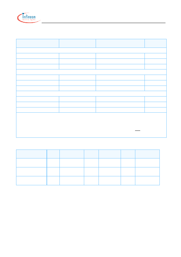
1.1 Ordering Information
1.2 Address Format
Type & Partnumber
Compliance Code
Description
SDRAM
Technology
PC2-3200 (DDR2-400):
HYS72T32000GR-5-A
PC2-3200R-33310-A
one rank 256 MB Reg. DIMM
256 Mbit (x8)
HYS72T64020GR-5-A
PC2-3200R-33310-B
two ranks 512 MB Reg. DIMM
256 Mbit (x8)
HYS72T64001GR-5-A
PC2-3200R-33310-C
one ranks 512 MB Reg.DIMM
256 Mbit (x4)
PC2-4200 (DDR2-533):
HYS72T32000GR-3.7-A
PC2-4200R-44410-A
one rank 256 MB Reg. DIMM
256 Mbit (x8)
HYS72T64020GR-3.7-A
PC2-4200R-44410-B
two ranks 512 MB Reg. DIMM
256 Mbit (x8)
HYS72T64001GR-3.7-A
PC2-4200R-44410-C
one ranks 512 MB Reg.DIMM
256 Mbit (x4)
PC2-5300 (DDR2-667):
HYS72T32000GR-3-A
PC2-5300R-44410-A
one rank 256 MB Reg. DIMM
256 Mbit (x8)
HYS72T64020GR-3-A
PC2-5300R-44410-B
two ranks 512 MB Reg. DIMM
256 Mbit (x8)
HYS72T64001GR-3-A
PC2-5300R-44410-C
one ranks 512 MB Reg.DIMM
256 Mbit (x4)
Notes:
1. All part numbers end with a place code, designating the silicon die revision. Example: HYS 72T32000GR-5-A, indicating
Rev. A dies are used for DDR2 SDRAM components. For all INFINEON DDR2 module and component nomenclature see
section 8 of this datasheet.
2. The Compliance Code is printed on the module label and describes the speed grade, f.e. "PC2-4200R-44410-C", where
4200R means Registered DIMM modules with 4.26 GB/sec Module Bandwidth and "44410" means CAS latency = 4, trcd
latency = 4 and trp latency = 4 using the latest JEDEC SPD Revision 1.0 and produced on the Raw Card "C".
Part Number
DIMM
Density
Organization
Memory
Ranks
DDR2-
SDRAMs
# of
SDRAMs
# of row/bank/
column bits
HYS72T32000GR
256 MB
32Mb
◊
72
1
(256Mb)
32Mb
◊
8
9
13/2/10
HYS72T64020GR
512 MB
2 x 32Mb
◊
72
2
(256Mb)
32Mb
◊
8
18
13/2/10
HYS72T64001GR-
512 MB
64Mb x 72
1
(256Mb)
64Mb
◊
4
18
13/2/11
HYS72Txx0xxGR
Registered DDR2 SDRAM-Modules
INFINEON Technologies
4
2.04
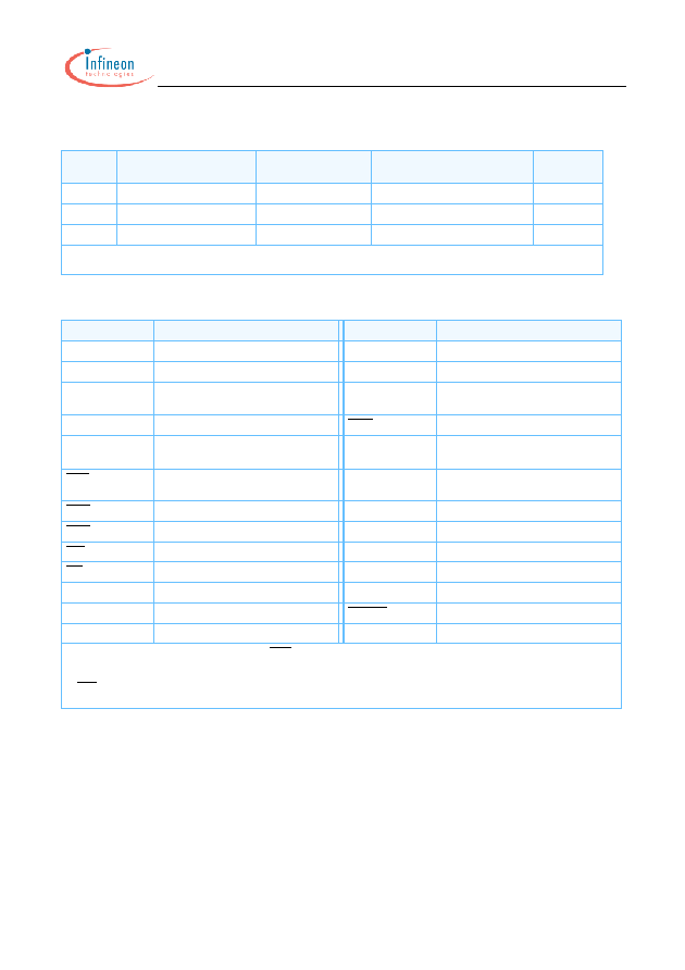
1.3 Components on Modules and RawCard
1.4 Pin Definition and Function
DIMM
Density
DRAM components
reference datasheet
PLL
Register
Raw Card
256 MB
HYB18T256800AC
1:10, 1.8V, CU877
1:1 25-bit 1.8V SSTU32864
A
512 MB
HYB18T256800AC
1:10, 1.8V, CU877
1:2 14-bit 1.8V SSTU32864
B
512 MB
HYB18T256400AC
1:10, 1.8V, CU877
1:2 14-bit 1.8V SSTU32864
C
For a detailed description of all functionalities of the DRAM components on these modules see the referenced component
datasheet
Pin Name
Description
Pin Name
Description
A[12:0]
Row Address Inputs
CB[7:0]
DIMM ECC Check Bits
A11, A[9:0]
Column Address Inputs
4)
DQS[8:0]
SDRAM low data strobes
A10/AP
Column Address Input for Auto-
Precharge
DM[8:0] /
DQS[17:9]
SDRAM low data mask/
high data strobes
BA[1:0]
SDRAM Bank Selects
DQS[17:0]
SDRAM differential data strobes
CK0
Clock input
(positive line of differential pair)
SCL
Serial bus clock
CK0
Clock input
(negative line of differential pair)
SDA
Serial bus data line
RAS
Row Address Strobe
SA[2:0]
slave address select
CAS
Column Address Strobe
V
DD
Power (+ 1.8 V)
WE
Read/Write Input
V
REF
I/O reference supply
CS[1:0]
Chip Selects
3)
V
SS
Ground
CKE[1:0]
Clock Enable
3)
V
DDSPD
EEPROM power supply
ODT[1:0]
Active termination control lines
1) 3)
RESET
Register and PLL control pin
2)
DQ[63:0]
Data Input/Output
NC
No connection
1) Active termination only applies to DQ, DQS, DQS and DM signals
2) When low, all register outputs will be driven low and the PLL clocks to the DRAM and registers will be set to low levels (the
PLL will remain synchronized with the input clock
3) CS1, ODT1 and CKE1 are used on dual rank modules only
4) Column address A11 is used on modules based on x4 organised 256Mb DDR2 components only.