INFINEON Technologies
1
9.01
HYS 72Vx2xxGR
PC100 Registered SDRAM-Modules
3.3 V 168-pin Registered PC100 SDRAM Modules
64 MB, 128 MB, 256 MB, 512 MB & 1 GB Densities
The HYS 72Vx2x0GR family are industry standard 168-pin 8-byte Dual in-line Memory Modules
(DIMMs) which are organized as 8M
◊
72, 16M
◊
72, 32M
◊
72, 64M
◊
72 & 128M
◊
72 high speed
memory arrays designed with Synchronous DRAMs (SDRAMs) for ECC applications. The 32M x 72
(256MByte) registered DIMM module is available in two versions (12 or 13 row addresses). All
control and address signals are registered on-DIMM and the design incorporates a PLL circuit for
the Clock inputs. Use of an on-board register reduces capacitive loading on the input signals but are
delayed by one cycle in arriving at the SDRAM devices. Decoupling capacitors are mounted on the
PC board. The DIMMs use a serial presence detects scheme implemented via a serial E
2
PROM
using the 2-pin I
2
C protocol. The first 128 bytes are utilized by the DIMM manufacturer and the
second 128 bytes are available to the end user. All Infineon 168-pin DIMMs provide a high
performance, flexible 8-byte interface in a 133.35 mm long footprint.
∑ 168-pin JEDEC Standard, Registered 8 Byte
Dual-In-Line SDRAM Module
for PC and Server main memory applications
∑ One bank 8M
◊
72, 16M
◊
72, 32M
◊
72 and
64M
◊
72 organization,
two bank 128M
◊
72 organization
∑ Optimized for ECC applications with very low
input capacitances
∑ Programmed Latencies:
∑ Single + 3.3 V (
±
0.3 V) power supply
∑ Programmable CAS Latency, Burst Length,
and Wrap Sequence (Sequential &
Interleave)
∑ Auto Refresh (CBR) and Self Refresh
∑ All inputs and outputs are LVTTL compatible
∑ Serial Presence Detect with E
2
PROM
∑ Utilizes SDRAMs in TSOPII-54 packages
with registers and PLL.
The two bank module uses stacked TSOP54
packages.
∑ Card Size: 133.35 mm
◊
38.1 mm/43.18 mm
with Gold contact pads (JEDEC MO-161)
∑ This specification follows INTEL's "PC
SDRAM Registered DIMM Specification"
Rev. 1.2
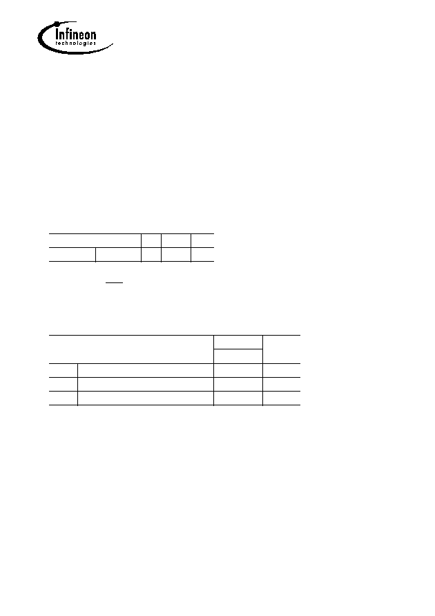
Product Speed
CL
t
RCD
t
RP
-8
PC100
2
2
2
∑ Performance:
-8
Unit
PC100
f
CK
Clock Frequency (max.)
100
MHz
t
CK
Clock Cycle Time (min.)
10
ns
t
AC
Clock Access Time (min.)
6
ns

HYS 72Vx2xxGR
PC100 Registered SDRAM-Modules
INFINEON Technologies
2
9.01
Note: All part numbers end with a place code (not shown), designating the die revision. Consult
factory for current revision. Example: HYS 64V8200GR-8-C2, indicating Rev. C2 dies are
used for SDRAM components.
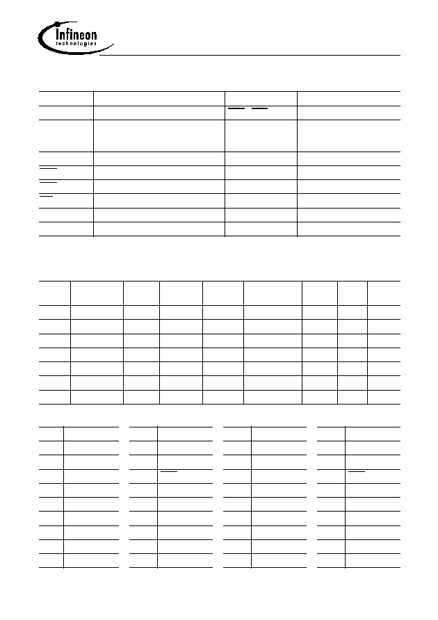
Ordering Information
Type
Compliance
Code
Description
SDRAM
Technology
HYS 72V8200GR-8-C
HYS 72V8200GR-8-E
PC100-222-622R one bank 64 MB Reg. DIMM
64 MBit (x8)
HYS 72V16200GR-8-C
HYS 72V16200GR-8-E
PC100-222-622R one bank 128 MB Reg. DIMM
64 MBit (x4)
HYS 72V16201GR-8-C2
PC100-222-622R one bank 128 MB Reg. DIMM
128 MBit (x8)
HYS 72V32201GR-8-C2
PC100-222-622R one bank 256 MB Reg. DIMM
128 MBit (x4)
HYS 72V32200GR-8-C2
PC100-222-622R one bank 256 MB Reg. DIMM
256 MBit (x8)
HYS 72V64200GR-8-C2
PC100-222-622R one bank 512 MB Reg. DIMM
256 MBit (x4)
HYS 72V128220GR-8-C2 PC100-222-622R two bank 1 GByte Reg. DIMM
256 MBit
(x4 stacked)
HYS 72Vx2xxGR
PC100 Registered SDRAM-Modules
INFINEON Technologies
3
9.01
*) note : To confirm to this specification, motherboards must pull this pin to high state or no connect.
Pin Definitions and Functions
A0 - A11, A12 Address Inputs
DQMB0 - DQMB7 Data Mask
BA0, BA1
Bank Selects
CS0 - CS3
Chip Select
DQ0 - DQ63
Data Input/Output
REGE *)
Register Enable
"H" or N.C = registered mode
"L" = buffered mode
CB0 - CB7
Check Bits (x72 organization only)
V
DD
Power (+ 3.3 V)
RAS
Row Address Strobe
V
SS
Ground
CAS
Column Address Strobe
SCL
Clock for Presence Detect
WE
Read/Write Input
SDA
Serial Data Out
CKE0
Clock Enable
N.C.
No Connection
CLK0 - CLK3
Clock Input
≠
≠
Address Format
Density Organization Memory
Banks
SDRAMs
# of
SDRAMs
# of row/bank/
columns bits
Refresh Period Interval
64 MB
8M
◊
72
1
8M
◊
8
9
12/2/9
4k
64 ms 15.6
µ
s
128 MB 16M
◊
72
1
16M
◊
4
18
12/2/10
4k
64 ms 15.6
µ
s
128 MB 16M
◊
72
1
16M x 8
9
12/2/10
4k
64 ms 15.6
µ
s
256 MB 32M
◊
72
1
32M
◊
4
18
12/2/11
4k
64 ms 15.6
µ
s
256 MB 32M
◊
72
1
32M
◊
8
9
13/2/10
8k
64 ms 7.8
µ
s
512 MB 64M
◊
72
1
64M
◊
4
18
13/2/11
8k
64 ms 7.8
µ
s
1 GB
128M
◊
72
2
64M
◊
4
36
13/2/11
8k
64 ms 7.8
µ
s
Pin Configuration
PIN# Symbol
PIN#
Symbol
PIN#
Symbol
PIN#
Symbol
1
V
SS
43
V
SS
85
V
SS
127
V
SS
2
DQ0
44
DU
86
DQ32
128
CKE0
3
DQ1
45
CS2
87
DQ33
129
CS3
4
DQ2
46
DQMB2
88
DQ34
130
DQMB6
5
DQ3
47
DQMB3
89
DQ35
131
DQMB7
6
V
DD
48
DU
90
V
DD
132
N.C.
7
DQ4
49
V
DD
91
DQ36
133
V
DD
8
DQ5
50
N.C.
92
DQ37
134
N.C.
9
DQ6
51
N.C.
93
DQ38
135
N.C.

HYS 72Vx2xxGR
PC100 Registered SDRAM-Modules
INFINEON Technologies
4
9.01
10
DQ7
52
CB2
94
DQ39
136
CB6
11
DQ8
53
CB3
95
DQ40
137
CB7
12
V
SS
54
V
SS
96
V
SS
138
V
SS
13
DQ9
55
DQ16
97
DQ41
139
DQ48
14
DQ10
56
DQ17
98
DQ42
140
DQ49
15
DQ11
57
DQ18
99
DQ43
141
DQ50
16
DQ12
58
DQ19
100
DQ44
142
DQ51
17
DQ13
59
V
DD
101
DQ45
143
V
DD
18
V
DD
60
DQ20
102
V
DD
144
DQ52
19
DQ14
61
N.C.
103
DQ46
145
N.C.
20
DQ15
62
DU
104
DQ47
146
DU
21
CB0
63
N.C.
105
CB4
147
REGE
22
CB1
64
V
SS
106
CB5
148
V
SS
23
V
SS
65
DQ21
107
V
SS
149
DQ53
24
N.C.
66
DQ22
108
N.C.
150
DQ54
25
N.C.
67
DQ23
109
N.C.
151
DQ55
26
V
DD
68
V
SS
110
V
DD
152
V
SS
27
WE
69
DQ24
111
CAS
153
DQ56
28
DQMB0
70
DQ25
112
DQMB4
154
DQ57
29
DQMB1
71
DQ26
113
DQMB5
155
DQ58
30
CS0
72
DQ27
114
CS1
156
DQ59
31
DU
73
V
DD
115
RAS
157
V
DD
32
V
SS
74
DQ28
116
V
SS
158
DQ60
33
A0
75
DQ29
117
A1
159
DQ61
34
A2
76
DQ30
118
A3
160
DQ62
35
A4
77
DQ31
119
A5
161
DQ63
36
A6
78
V
SS
120
A7
162
V
SS
37
A8
79
CLK2
121
A9
163
CLK3
38
A10 (AP)
80
N.C.
122
BA0
164
N.C.
39
BA1
81
WP
123
A11
165
SA0
40
V
DD
82
SDA
124
V
DD
166
SA1
41
V
DD
83
SCL
125
CLK1
167
SA2
42
CLK0
84
V
DD
126
A12
168
V
DD
Pin Configuration (cont'd)
PIN# Symbol
PIN#
Symbol
PIN#
Symbol
PIN#
Symbol

HYS 72Vx2xxGR
PC100 Registered SDRAM-Modules
INFINEON Technologies
5
9.01
Block Diagram: One Bank 8M x 72, 16M x 72 & 32M x 72 SDRAM DIMM Modules
HYS 72V8200GR, HYS72V16201GR and HYS 72V32200GR Using x8 Organized SDRAMs
SPB04130-2
DQ0-DQ7
CS
D0
DQ0-DQ7
RDQMB0
RCS0
DQ0-DQ7
CS
D4
DQ32-DQ39
CLK0
12 pF
PLL
SDRAMs D0-D8
CLK1, CLK2, CLK3
12 pF
R
egi
s
t
er
CS0/CS2
DQMB0-7
BA0, BA1
A0-A11,12*
)
RAS
CAS
CKE0
WE
RCS0/RCS2
RDQMB0-7
RBA0, RBA1
RA0-11,12
RRAS
RCAS
RCKE0
RWE
REGE
10 k
SDRAMs D0-D8
SDRAMs D0-D8
SDRAMs D0-D8
SDRAMs D0-D8
SDRAMs D0-D8
SDRAMs D0-D8
SA0
SDA
SA0
SA1
SA1
SA2
SA2
SCL
SCL
WP
47 k
E
2
PROM
(256 word x 8 Bit)
V
C C
V
S S
C
D0-D8, Reg., DLL
D0-D8, Reg., DLL
Notes:
1 )
DQ wirding may differ from that
decribed in this drawing;
however DQ/DQB relationship
must be maintained as shown
2 )
All resistors are 10
unless
otherwise noted
*
)
A12 is only for 32 M x 72
organisation
V
C C
DQM
RDQMB4
DQM
DQ0-DQ7
CS
D1
DQ8-DQ15
RDQMB1
DQ0-DQ7
CS
D5
DQ40-DQ47
DQM
RDQMB5
DQM
DQ0-DQ7
CS
D8
DQM
WE
DQ0-DQ7
CS
D2
DQ16-DQ23
RDQMB2
RCS2
DQ0-DQ7
CS
D6
DQ48-DQ55
DQM
RDQMB4
DQM
DQ0-DQ7
CS
D3
DQ24-DQ31
RDQMB3
DQ0-DQ7
CS
D7
DQ56-DQ63
DQM
RDQMB7
DQM
CB7
CB0-