 | –≠–ª–µ–∫—Ç—Ä–æ–Ω–Ω—ã–π –∫–æ–º–ø–æ–Ω–µ–Ω—Ç: IGW25T120 | –°–∫–∞—á–∞—Ç—å:  PDF PDF  ZIP ZIP |

IGW25T120
^
TrenchStop Series
Power Semiconductors
1
Preliminary / Rev. 1 Jul-02
Low Loss IGBT in Trench and Fieldstop
technology
∑
Approx. 1.0V reduced V
CE(sat)
compared to BUP314
∑
Short circuit withstand time ≠ 10
µ
s
∑
Designed for :
- Frequency Converters
- Uninterrupted Power Supply
∑
Trench and Fieldstop technology for 1200 V applications offers :
- very tight parameter distribution
- high ruggedness, temperature stable behavior
∑
NPT technology offers easy parallel switching capability due to
positive temperature coefficient in V
CE(sat)
∑
Low
EMI
∑
Low Gate Charge
∑
Complete product spectrum and PSpice Models :
http://www.infineon.com/igbt/
Type
V
CE
I
C
V
CE(sat
),Tj=25∞C
T
j,max
Package
Ordering Code
IGW25T120
1200V
25A
1.7V
150
∞
C
TO-247AC
Q67040-S4517
Maximum Ratings
Parameter
Symbol
Value
Unit
Collector-emitter voltage
V
C E
1200
V
DC collector current
T
C
= 25
∞
C
T
C
= 100
∞
C
I
C
50
25
Pulsed collector current,
t
p
limited by
T
jmax
I
C p u l s
75
Turn off safe operating area
V
CE
1200V,
T
j
150
∞
C
-
75
A
Gate-emitter voltage
V
G E
±
20
V
Short circuit withstand time
1)
V
GE
= 15V,
V
CC
1200V,
T
j
150
∞
C
t
S C
10
µ
s
Power dissipation
T
C
= 25
∞
C
P
t o t
190
W
Operating junction temperature
T
j
-40...+150
Storage temperature
T
s t g
-55...+150
Soldering temperature, 1.6mm (0.063 in.) from case for 10s
-
260
∞
C
1)
Allowed number of short circuits: <1000; time between short circuits: >1s.
P-TO-247-3-1
(TO-247AC)
G
C
E

IGW25T120
^
TrenchStop Series
Power Semiconductors
2
Preliminary / Rev. 1 Jul-02
Thermal Resistance
Parameter
Symbol
Conditions
Max. Value
Unit
Characteristic
IGBT thermal resistance,
junction ≠ case
R
t h J C
0.65
Thermal resistance,
junction ≠ ambient
R
t h J A
TO-247AC
40
K/W
Electrical Characteristic,
at
T
j
= 25
∞
C, unless otherwise specified
Value
Parameter
Symbol
Conditions
min.
typ.
max.
Unit
Static Characteristic
Collector-emitter breakdown voltage
V
( B R ) C E S
V
G E
=0V,
I
C
=500
µ
A
1200
-
-
Collector-emitter saturation voltage
V
C E ( s a t )
V
G E
= 15V,
I
C
=25A
T
j
=25
∞
C
T
j
=125
∞
C
T
j
=150
∞
C
-
-
-
1.7
2.0
2.2
2.2
-
-
Gate-emitter threshold voltage
V
G E ( t h )
I
C
=1m A,
V
C E
=
V
G E
5.0
5.8
6.5
V
Zero gate voltage collector current
I
C E S
V
C E
=1200V
,
V
G E
=0V
T
j
=25
∞
C
T
j
=150
∞
C
-
-
-
-
0.25
2.5
mA
Gate-emitter leakage current
I
G E S
V
C E
=0V,
V
G E
=20V
-
-
600
nA
Transconductance
g
f s
V
C E
=20V,
I
C
=25A
-
16
-
S
Integrated gate resistor
R
G i n t
8

IGW25T120
^
TrenchStop Series
Power Semiconductors
3
Preliminary / Rev. 1 Jul-02
Dynamic Characteristic
Input capacitance
C
i s s
-
1860
-
Output capacitance
C
o s s
-
96
-
Reverse transfer capacitance
C
r s s
V
C E
=25V,
V
G E
=0V,
f
=1MHz
-
82
-
pF
Gate charge
Q
G a t e
V
C C
=960V,
I
C
=25A
V
G E
=15V
-
155
-
nC
Internal emitter inductance
measured 5mm (0.197 in.) from case
L
E
T O-247AC
-
-
13
nH
Short circuit collector current
1)
I
C ( S C )
V
G E
=15V,
t
S C
10
µ
s
V
C C
= 600V,
T
j
= 25
∞
C
-
150
-
A
Switching Characteristic, Inductive Load,
at
T
j
=25
∞
C
Value
Parameter
Symbol
Conditions
min.
typ.
max.
Unit
IGBT Characteristic
Turn-on delay time
t
d ( o n )
-
50
-
Rise time
t
r
-
30
-
Turn-off delay time
t
d ( o f f )
-
560
-
Fall time
t
f
-
70
-
ns
Turn-on energy
E
o n
-
2.0
-
Turn-off energy
E
o f f
-
2.2
-
Total switching energy
E
t s
T
j
=25
∞
C,
V
C C
=600V,
I
C
=25A
V
G E
=- 15/15V,
R
G
=22
,
L
2 )
=180nH,
C
2 )
=39pF
Energy losses include
"tail" and diode
reverse recovery.
-
4.2
-
mJ
Switching Characteristic, Inductive Load,
at
T
j
=150
∞
C
Value
Parameter
Symbol
Conditions
min.
typ.
max.
Unit
IGBT Characteristic
Turn-on delay time
t
d ( o n )
-
50
-
Rise time
t
r
-
32
-
Turn-off delay time
t
d ( o f f )
-
660
-
Fall time
t
f
-
130
-
ns
Turn-on energy
E
o n
-
3.0
-
Turn-off energy
E
o f f
-
4.0
-
Total switching energy
E
t s
T
j
=150
∞
C
V
C C
=600V,
I
C
=25A,
V
G E
=- 15/15V,
R
G
= 22
,
L
2 )
=180nH,
C
2 )
=39pF
Energy losses include
"tail" and diode
reverse recovery.
-
7.0
-
mJ
1)
Allowed number of short circuits: <1000; time between short circuits: >1s.
2)
Leakage inductance
L
and Stray capacity
C
due to dynamic test circuit in Figure E.
IGW25T120
^
TrenchStop Series
Power Semiconductors
4
Preliminary / Rev. 1 Jul-02
I
C
,
COLLE
CT
OR CURRE
N
T
10Hz
100Hz
1kHz
10kHz
100kHz
0A
10A
20A
30A
40A
50A
60A
70A
T
C
=110∞C
T
C
=80∞C
I
C
,
COLLE
CT
OR CURRE
N
T
1V
10V
100V
1000V
0,1A
1A
10A
DC
10µs
t
p
=3µs
50µs
500µs
20ms
150µs
f
,
SWITCHING FREQUENCY
V
CE
,
COLLECTOR
-
EMITTER VOLTAGE
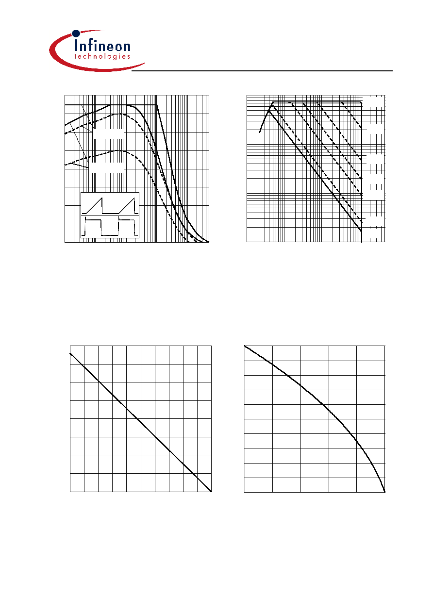
Figure 1. Collector current as a function of
switching frequency
(
T
j
150
∞
C,
D =
0.5,
V
CE
= 600V,
V
GE
= 0/+15V,
R
G
= 22
)
Figure 2. Safe operating area
(
D =
0,
T
C
= 25
∞
C,
T
j
150
∞
C;
V
GE
=15V)
P
tot
,
PO
W
E
R
D
I
SS
IP
AT
IO
N
25∞C
50∞C
75∞C
100∞C
125∞C
0W
50W
100W
150W
I
C
,
COLLE
CT
OR CURRE
N
T
25∞C
75∞C
125∞C
0A
10A
20A
30A
40A
T
C
,
CASE TEMPERATURE
T
C
,
CASE TEMPERATURE
Figure 3. Power dissipation as a function of
case temperature
(
T
j
150
∞
C)
Figure 4. Collector current as a function of
case temperature
(
V
GE
15V,
T
j
150
∞
C)
I
c
I
c

IGW25T120
^
TrenchStop Series
Power Semiconductors
5
Preliminary / Rev. 1 Jul-02
I
C
,
COLLE
CT
OR CURRE
N
T
0V
1V
2V
3V
4V
5V
6V
0A
10A
20A
30A
40A
50A
60A
70A
15V
7V
9V
11V
13V
V
GE
=17V
I
C
,
COLLE
CT
OR CURRE
N
T
0V
1V
2V
3V
4V
5V
6V
0A
10A
20A
30A
40A
50A
60A
70A
15V
7V
9V
11V
13V
V
GE
=17V
V
CE
,
COLLECTOR
-
EMITTER VOLTAGE
V
CE
,
COLLECTOR
-
EMITTER VOLTAGE
Figure 5. Typical output characteristic
(
T
j
= 25∞C)
Figure 6. Typical output characteristic
(
T
j
= 150∞C)
I
C
,
COLLE
CT
OR CURRE
NT
0V
2V
4V
6V
8V
10V
12V
0A
10A
20A
30A
40A
50A
60A
70A
25∞C
T
J
=150∞C
V
C
E
(s
at),
COLLE
CTOR
-
E
M
I
TT SAT
U
R
A
T
I
O
N
VO
L
T
AG
E
-50∞C
0∞C
50∞C
100∞C
0,0V
0,5V
1,0V
1,5V
2,0V
2,5V
3,0V
I
C
=25A
I
C
=50A
I
C
=15A
I
C
=8A
V
GE
,
GATE-EMITTER VOLTAGE
T
J
,
JUNCTION TEMPERATURE
Figure 7. Typical transfer characteristic
(V
CE
=20V)
Figure 8. Typical collector-emitter
saturation voltage as a function of
junction temperature
(
V
GE
= 15V)